Overview
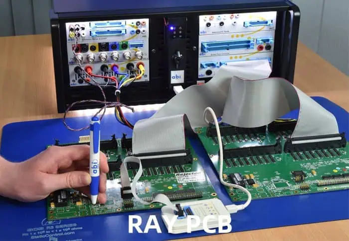
Boundary Scan Testing utilizing JTAG (Joint Test Action Group) technology provides an advanced, non-intrusive method for testing digital circuits on printed circuit boards. This IEEE 1149.1 standard-compliant testing approach enables comprehensive fault detection and diagnosis without requiring physical test probes or bed-of-nails fixtures.
Key Features
Non-Invasive Testing: Test digital components through their built-in JTAG interface without physical contact to circuit nodes, eliminating the need for expensive test fixtures and reducing potential damage to delicate components.
High Test Coverage: Achieve up to 95% fault coverage on boundary scan-enabled devices, detecting opens, shorts, stuck-at faults, and component failures that traditional in-circuit testing might miss.
Cost-Effective Solution: Reduce testing infrastructure costs by eliminating complex mechanical fixtures while providing faster test execution and simplified test program development.
Advanced Diagnostics: Pinpoint exact fault locations with detailed failure analysis, including specific pin-level fault identification and comprehensive reporting capabilities.
Technical Capabilities
- Interconnect Testing: Verify connections between JTAG-enabled components, detecting opens and shorts in PCB traces
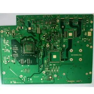
- Component Verification: Confirm proper installation and functionality of boundary scan devices including processors, FPGAs, memory controllers, and ASICs
- In-System Programming: Program and configure devices through the JTAG chain without removing components from the board
- Cluster Testing: Test multiple boards simultaneously through JTAG chain multiplexing
- Mixed-Signal Support: Combined boundary scan and traditional testing for comprehensive coverage of both digital and analog circuits
Applications
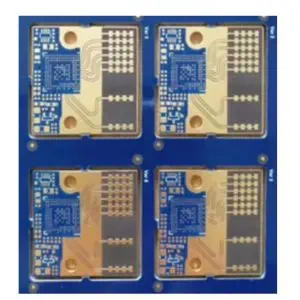
- High-density PCB assemblies in telecommunications equipment
- Automotive electronic control units (ECUs)
- Aerospace and defense systems
- Medical device electronics
- Industrial control systems
- Consumer electronics with complex digital architectures
Benefits
Faster Time-to-Market: Rapid test development and execution compared to traditional methods, with automated test generation capabilities.
Improved Quality: Enhanced fault detection accuracy and repeatable testing results ensure higher product reliability.
Manufacturing Flexibility: Easily adaptable to design changes without requiring new test fixtures or extensive reprogramming.
Future-Proof Technology: IEEE standard compliance ensures long-term compatibility and support across diverse component ecosystems.
Transform your PCB testing strategy with boundary scan technology that delivers superior fault coverage, reduced testing costs, and improved manufacturing efficiency.