Ultimate High-Density Interconnect Solution for Advanced Electronics
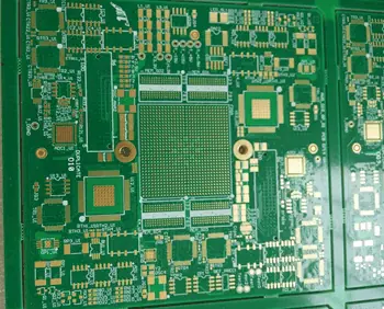
Our 64-layer PCB fabrication service delivers the highest level of circuit density and complexity available in modern electronics manufacturing. Engineered for cutting-edge applications where space constraints and performance demands push the boundaries of traditional PCB technology.
Key Features
Maximum Layer Count: 64 conductive layers with precision-controlled impedance and minimal signal loss, enabling unprecedented circuit density in compact form factors.
Advanced Materials: Utilizing low-loss dielectric materials and high-performance copper foils optimized for high-frequency applications and thermal management.
Micro-Via Technology: Sequential build-up process with micro-vias as small as 0.1mm diameter, enabling dense interconnections between layers while maintaining signal integrity.
Precision Manufacturing: Tolerances held to ±0.05mm with advanced drilling and plating processes ensuring reliable via connections across all 64 layers.
Controlled Impedance: Precisely matched impedance characteristics across all signal layers, critical for high-speed digital and RF applications.
Technical Specifications
- Layer Count: Up to 64 layers
- Minimum Trace Width: 0.075mm (3 mil)
- Minimum Via Size: 0.1mm diameter
- Board Thickness: 2.5-6.0mm depending on layer stackup
- Dielectric Materials: FR-4, polyimide, and low-loss specialized substrates
- Copper Weight: 0.5-2.0 oz per layer
- Surface Finish: HASL, ENIG, OSP, or immersion silver options
Applications
Ideal for aerospace and defense systems, high-performance computing, telecommunications infrastructure, medical devices, and advanced automotive electronics where maximum functionality must be achieved in minimal space.
Quality Assurance
Every 64-layer PCB undergoes comprehensive electrical testing, impedance verification, and thermal cycling validation to ensure reliability in demanding applications. Full traceability and documentation provided for critical applications.
Lead Time: 15-20 business days depending on complexity and quantity.
Transform your most challenging circuit designs into reality with our 64-layer PCB fabrication capabilities – where engineering excellence meets manufacturing precision.