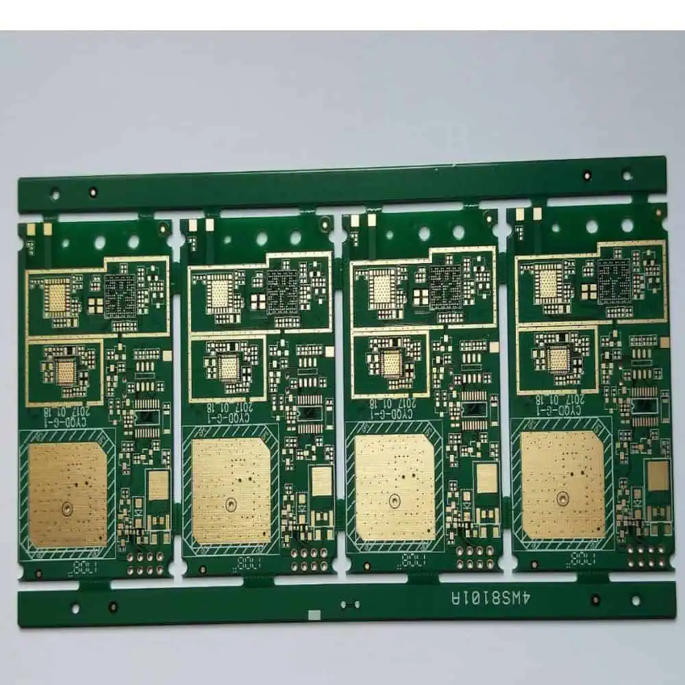
The Advantages of 6-Layer PCBs
-
Increased Circuit Density: As electronic devices become more compact and feature-rich, the demand for higher circuit density increases. A 6-layer PCB allows for more components and traces to be packed into a smaller area, making it ideal for complex designs.
-
Improved Signal Integrity: With six layers, designers have more flexibility in routing signals. This allows for better separation of high-speed signals, power planes, and ground planes, resulting in reduced electromagnetic interference (EMI) and improved signal integrity.
-
Enhanced Power Distribution: Dedicated power and ground planes can be incorporated, ensuring stable power delivery across the board. This is particularly important for designs with multiple voltage requirements or high current demands.
-
Better Thermal Management: Multiple layers provide more copper for heat dissipation, which is crucial for high-power designs or applications in challenging environments.
-
Flexibility in Design: The additional layers offer more options for designers to optimize their layouts, potentially reducing the overall board size or improving performance.
The Benefits of Halogen-Free PCBs
-
Environmental Responsibility: Halogen-free PCBs reduce the environmental impact of electronic waste. When incinerated, they produce fewer toxic substances compared to traditional PCBs containing halogens.
-
Compliance with Regulations: Many countries and industries have implemented regulations limiting the use of halogenated compounds. Using halogen-free PCBs ensures compliance with these standards, such as the EU’s RoHS directive.
-
Improved Safety: In the event of a fire, halogen-free PCBs produce less toxic smoke, reducing health risks to individuals in the vicinity.
-
Enhanced Reliability: Some studies suggest that halogen-free materials can offer improved reliability under certain conditions, such as high humidity environments.
-
Market Advantage: As consumers become more environmentally conscious, products using halogen-free PCBs can have a marketing edge.
Combining 6 Layers and Halogen-Free Materials
When we combine the advantages of a 6-layer design with halogen-free materials, we create a PCB that is both high-performance and environmentally responsible. This combination is particularly beneficial in several scenarios:
-
Complex, High-Density Designs: Applications requiring numerous components and intricate routing can benefit from the additional layers while meeting environmental standards.
-
High-Speed Applications: The ability to control impedance and reduce crosstalk in a 6-layer design, coupled with the potentially superior electrical properties of some halogen-free materials, can be advantageous for high-speed circuits.
-
Medical Devices: The medical industry often requires both high reliability and compliance with strict environmental and safety regulations, making 6-layer halogen-free PCBs an excellent choice.
-
Aerospace and Defense: These sectors often need PCBs that can perform in harsh environments while meeting stringent regulatory requirements.
-
Consumer Electronics: As consumers become more environmentally conscious, using halogen-free materials in complex, feature-rich devices can be a selling point.
Challenges and Considerations
While 6-layer halogen-free PCBs offer numerous advantages, there are some challenges to consider:
-
Cost: Both the additional layers and halogen-free materials can increase the cost of PCB production. However, this may be offset by improved performance and regulatory compliance.
-
Design Complexity: More layers require careful consideration of signal integrity, impedance control, and thermal management.
-
Material Properties: Some halogen-free materials may have different electrical or thermal properties compared to traditional materials, requiring adjustments in the design process.
-
Manufacturing Process: Fabrication of 6-layer halogen-free PCBs may require specialized equipment or processes, potentially limiting manufacturing options.
In conclusion, designing a 6-layer halogen-free PCB represents a forward-thinking approach that balances high performance with environmental responsibility. While it presents some challenges, the benefits in terms of design flexibility, signal integrity, and regulatory compliance make it an attractive option for many modern electronic applications. As technology continues to advance and environmental concerns remain at the forefront, we can expect to see increased adoption of such designs across various industries.


