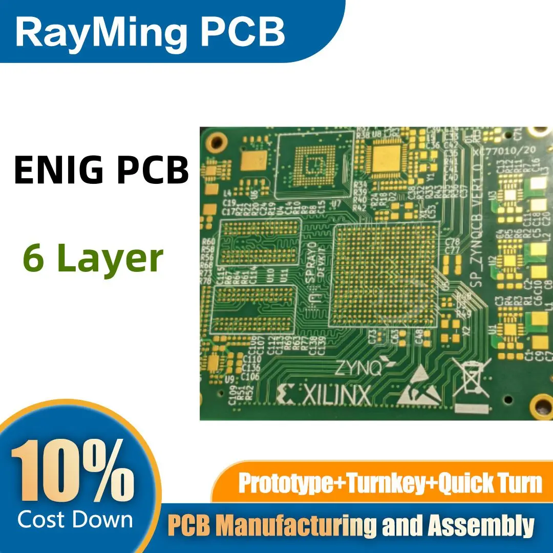
Six-layer Electroless Nickel Immersion Gold (ENIG) PCBs represent a high-performance configuration in printed circuit board manufacturing. Key features include:
-
Layer Structure: Six alternating layers of copper and insulating material, providing enhanced design complexity and signal integrity.
-
ENIG Finish: A surface treatment consisting of an electroless nickel layer (typically 3-6 µm) covered by a thin immersion gold layer (0.05-0.1 µm).
-
Design Flexibility: Allows for complex routing and high-density component placement across multiple layers.
-
Signal Integrity: Improved signal transmission and reduced electromagnetic interference due to the multi-layer structure.
-
Surface Characteristics:
- Excellent flatness for fine-pitch component placement
- Uniform surface finish across all layers
- Enhanced corrosion resistance and extended shelf life
-
Applications: Ideal for high-frequency circuits, telecommunications equipment, medical devices, and aerospace technology.
-
Manufacturing Process: Involves precise control of layer alignment, via formation, and ENIG plating to ensure uniform coverage and optimal performance.
-
Performance Benefits:
- Superior impedance control across all six layers
- Excellent solderability and wire bonding compatibility
- Suitable for both leaded and lead-free soldering processes
This configuration balances advanced electrical performance, reliability, and manufacturability, making it suitable for a wide range of demanding electronic applications.