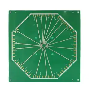
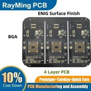
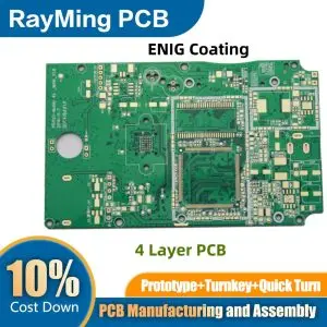
Six-layer PCBs with 2µ” (microinch) ENIG (Electroless Nickel Immersion Gold) plating represent a high-end configuration in printed circuit board manufacturing. Key aspects include:
-
Layer Structure: Six alternating layers of copper and insulating material, offering increased design complexity and signal integrity.
-
ENIG Plating: Consists of an electroless nickel layer followed by a thin immersion gold coating.
-
Thickness Specifications:
- Nickel layer: Typically 120-240µ” (3-6 µm)
- Gold layer: 2µ” (0.05 µm), providing optimal protection without excess material
-
Benefits of 2µ” Gold:
- Sufficient for excellent solderability and wire bonding
- Prevents gold embrittlement in solder joints
- Cost-effective compared to thicker gold layers
-
Applications: Ideal for high-frequency circuits, aerospace, medical devices, and telecommunications equipment.
-
Performance Characteristics:
- Enhanced signal integrity in complex, high-density designs
- Improved impedance control across all six layers
- Excellent flatness for fine-pitch component placement
-
Reliability: The precise 2µ” gold thickness ensures long-term protection against oxidation without compromising solderability or introducing potential reliability issues associated with excessive gold content.
This configuration balances advanced performance with cost-effectiveness in demanding electronic applications.


