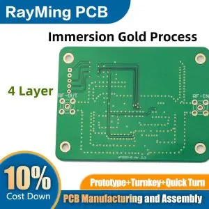
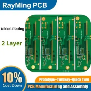
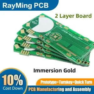
3μ” (3 microinches) Immersion Gold Thickness PCB refers to a printed circuit board finishing technique where a thin layer of gold is deposited on exposed copper surfaces. This process, known as ENIG (Electroless Nickel Immersion Gold), involves first plating a layer of nickel, followed by a thin gold coating. The “3μ”” specification indicates the thickness of the gold layer, which is approximately 0.076 micrometers.
This finish offers several advantages for PCB manufacturing:
- Excellent solderability and long shelf life
- Flat surface ideal for components with fine-pitch leads
- Suitable for wire bonding applications
- Resistant to oxidation and corrosion
- Compatible with lead-free soldering processes
The thin gold layer provides sufficient protection while keeping costs lower compared to thicker gold finishes. It’s widely used in high-reliability electronics, telecommunications, and aerospace applications. However, care must be taken during assembly to prevent excessive dissolution of the gold layer, which could expose the underlying nickel.


