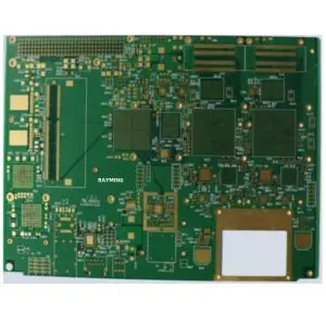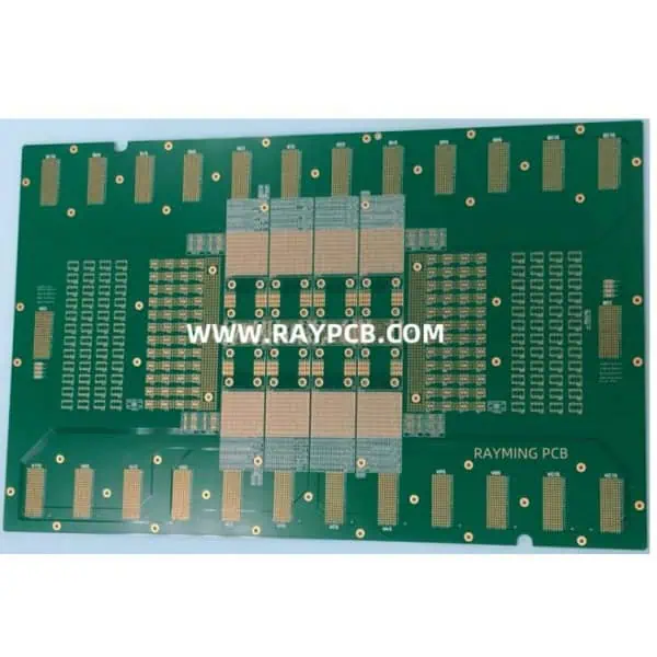
Our 32-layer PCB manufacturing service delivers the ultimate solution for high-density, high-performance electronic applications that demand exceptional signal integrity and compact design. These ultra-complex multilayer boards represent the pinnacle of PCB technology, engineered for the most demanding applications in telecommunications, aerospace, medical devices, and advanced computing systems.
Key Features:
- 32 conductive layers with precise impedance control and minimal signal loss
- Advanced HDI (High Density Interconnect) technology with microvias and blind/buried vias
- Superior signal integrity through optimized layer stackup and controlled dielectric properties
- Exceptional thermal management with integrated heat dissipation solutions
- Ultra-fine pitch capability supporting component densities up to 0.4mm BGA and beyond
- Multilayer shielding for EMI/EMC compliance and crosstalk elimination
Technical Specifications:
- Layer count: 32 layers maximum
- Minimum trace width: 0.075mm (3 mil)
- Minimum via size: 0.1mm (4 mil)
- Board thickness: 1.6mm – 6.0mm
- Copper weight: 0.5oz – 2oz per layer
- Dielectric materials: FR-4, Rogers, Polyimide, and specialized low-loss materials
- Surface finish: HASL, ENIG, OSP, Immersion Silver, Hard Gold
Applications:
- High-speed digital processors and GPUs
- RF/microwave communication systems
- Aerospace and defense electronics
- Medical imaging equipment
- 5G infrastructure and base stations
- High-performance computing servers
- Automotive ADAS and autonomous driving systems
Quality Assurance:
- IPC Class 2 and Class 3 compliance
- 100% electrical testing and impedance verification
- Advanced AOI (Automated Optical Inspection)
- Cross-sectional analysis and microsectioning
- Comprehensive design rule checking (DRC)
Manufacturing Capabilities:
- Lead time: 15-25 business days
- Minimum order quantity: 5 pieces
- Maximum panel size: 18″ x 24″
- Advanced sequential lamination process
- Precision drill registration and layer alignment
Our experienced engineering team provides comprehensive design support, including stackup optimization, signal integrity analysis, and thermal modeling to ensure your 32-layer PCB meets the most stringent performance requirements while maintaining manufacturing reliability and cost-effectiveness.