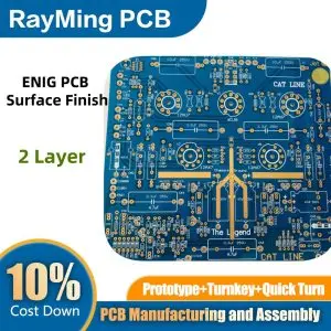
2 Layer Gold Plating on PCB refers to a surface finish technique applied to printed circuit boards with two conductive layers. This process involves depositing a layer of gold onto specific areas or the entire surface of the PCB.
The gold plating process typically involves:
- Cleaning the copper surface
- Applying a thin nickel layer as an undercoat (usually 3-5 microns thick)
- Electroplating gold onto the nickel layer (thickness varies based on requirements)
Benefits of gold plating include:
- Excellent corrosion resistance
- Superior electrical conductivity
- Enhanced solderability and wire bonding capability
- Long shelf life
- Ideal for high-frequency applications due to low signal loss
Gold plating thickness can vary:
- Soft gold: 0.1-1 micron, suitable for most applications
- Hard gold: 1-50 microns, used for wear-resistant contacts
While gold plating offers numerous advantages, it’s more expensive than other finishes. It’s commonly used in high-reliability electronics, aerospace, medical devices, and telecommunications equipment where performance and longevity are critical.