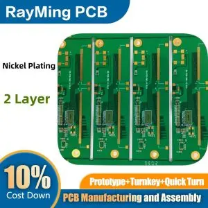
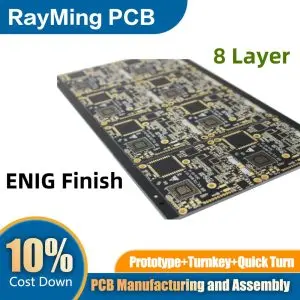
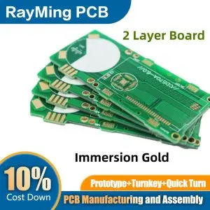
2 Layer ENIG Skip Plating PCB is a specialized printed circuit board manufacturing technique that combines the benefits of Electroless Nickel Immersion Gold (ENIG) finish with selective plating. In this process, certain areas of the PCB are intentionally left unplated, or “skipped,” during the ENIG application.
Skip plating is particularly useful when specific areas of the board need to remain copper-only, such as RF grounding planes or high-current carrying areas. This technique can enhance the PCB’s performance in applications where the characteristics of bare copper are preferred in certain locations.
The process involves carefully masking off the areas that should not receive the ENIG finish before applying the electroless nickel and immersion gold layers. This selective plating allows for greater design flexibility and can optimize the board’s electrical and thermal properties.
Skip plating in 2 Layer ENIG PCBs can offer several advantages:
- Improved RF performance in sensitive areas
- Better heat dissipation in high-power regions
- Cost reduction by minimizing the use of expensive metals in non-critical areas
- Enhanced functionality by allowing different surface properties on the same board
However, skip plating requires precise control during manufacturing to ensure clean boundaries between plated and unplated areas.


