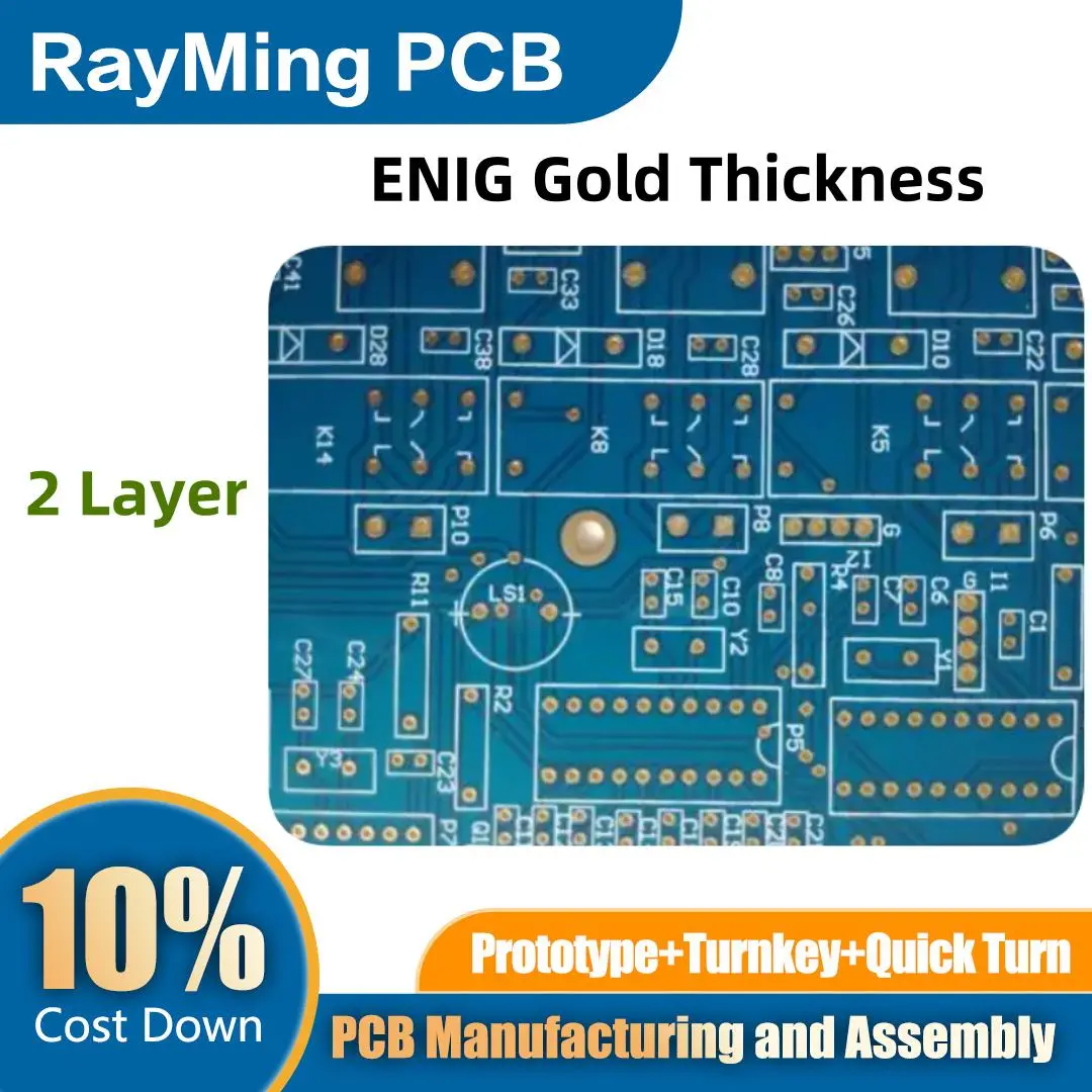
2 Layer ENIG (Electroless Nickel Immersion Gold) is a popular surface finish for printed circuit boards (PCBs), known for its excellent solderability and protection against oxidation. The gold thickness in ENIG is a critical parameter that affects both the performance and cost of the PCB.
Typically, the gold layer in 2 Layer ENIG PCBs ranges from 2 to 5 microinches (0.05 to 0.13 micrometers) thick. This thin layer of gold is deposited over a thicker layer of electroless nickel, which is usually between 120 to 240 microinches (3 to 6 micrometers) thick.
The gold thickness is crucial because it impacts several factors:
- Solderability: A thicker gold layer generally provides better initial solderability.
- Shelf life: More gold offers better protection against oxidation, extending the PCB’s shelf life.
- Wire bonding: Thicker gold layers are preferable for wire bonding applications.
- Cost: Gold is expensive, so thicker layers increase the overall cost of the PCB.
However, excessive gold thickness can lead to issues like embrittlement of solder joints due to the formation of gold-tin intermetallics. Therefore, maintaining the right balance is essential for optimal performance and cost-effectiveness in 2 Layer ENIG PCBs.


