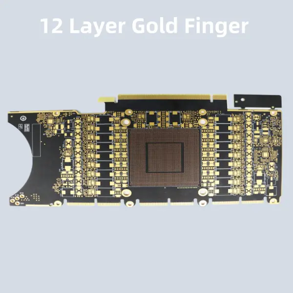
Designing a 12-Layer Graphics Card PCB
1. Requirements Gathering
- Define performance targets (e.g., memory bandwidth, power requirements)
- List all components (GPU, VRAM, VRMs, connectors, etc.)
- Determine thermal and power constraints
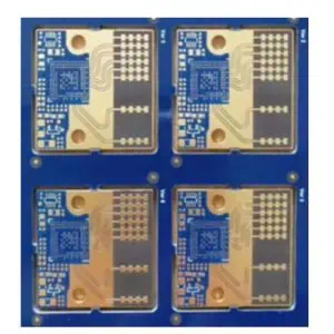
2. Component Selection
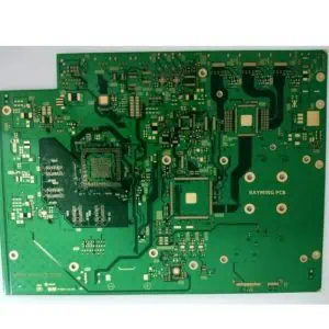
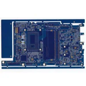
- Choose the GPU chip (e.g., NVIDIA or AMD)
- Select appropriate VRAM modules
- Determine power delivery components (MOSFETs, capacitors, inductors)
- Choose display output connectors (HDMI, DisplayPort, etc.)


3. Schematic Design
- Create a detailed circuit diagram
- Define all electrical connections between components
- Ensure proper power distribution and signal integrity
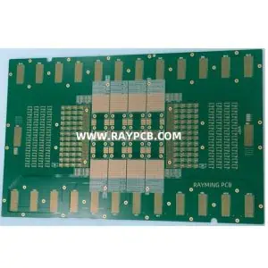
4. Layer Stack-up Planning
- Top Layer: Component placement and high-speed signals
- Ground Plane
- Power Plane
- Signal Layer 1
- Signal Layer 2
- Ground Plane
- Power Plane
- Signal Layer 3
- Signal Layer 4
- Ground Plane
- Power Plane
- Bottom Layer: Additional components and gold fingers
5. Component Placement
- Position GPU and VRAM for optimal heat dissipation
- Arrange VRMs close to power-hungry components
- Place decoupling capacitors near ICs
- Ensure proper clearance for cooling solutions
6. Routing
- Start with critical high-speed traces (e.g., memory interfaces)
- Route power and ground planes
- Implement differential pair routing for high-speed signals
- Maintain consistent trace widths and spacing
- Use vias judiciously, considering signal integrity
7. Power Integrity Analysis
- Simulate power delivery network
- Ensure voltage drops are within acceptable limits
- Add additional power/ground planes if necessary
8. Signal Integrity Analysis
- Perform simulations on critical traces
- Check for reflections, crosstalk, and electromagnetic interference
- Adjust trace lengths and routing as needed
9. Thermal Analysis
- Simulate heat distribution
- Identify potential hotspots
- Plan for thermal pads and heatsink attachment points
10. DRC and ERC
- Run Design Rule Checks (DRC) to ensure manufacturing compatibility
- Perform Electrical Rule Checks (ERC) to catch potential electrical issues
11. Documentation
- Generate detailed BOM (Bill of Materials)
- Create assembly drawings and instructions
- Prepare manufacturing files (Gerber files, drill files, etc.)
12. Prototyping and Testing
- Manufacture a small batch of prototype PCBs
- Assemble and test the prototypes
- Iterate on the design based on test results
13. Final Review and Approval
- Conduct a comprehensive design review
- Obtain necessary certifications (e.g., FCC, CE)
- Prepare for mass production
Remember: This is a highly simplified overview. Actual graphics card PCB design requires extensive expertise in electrical engineering, thermal management, and high-speed digital design.