Superior Performance for High-Density Applications
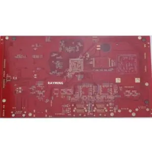
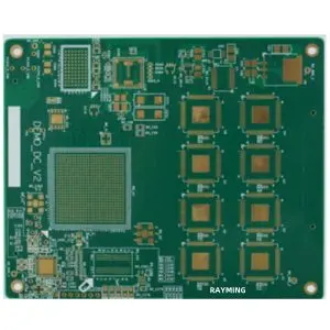
Our premium 12-layer PCB design and manufacturing service delivers exceptional reliability for your most demanding electronic applications. Engineered with precision, our 12-layer PCBs provide the perfect foundation for complex circuits requiring extensive routing capabilities, enhanced signal integrity, and optimal thermal management.
Key Features:
- Advanced 12-layer stackup design optimized for signal integrity
- High-density interconnect (HDI) compatible with microvias and buried/blind vias
- Superior impedance control (±5% tolerance) for critical high-speed signals
- Premium FR-4 or high-performance substrates available
- Comprehensive DFM (Design for Manufacturing) review included
- IPC Class 2 and Class 3 compliant manufacturing processes
- Available in standard and custom board dimensions
- Dedicated engineering support throughout your project lifecycle
Ideal Applications:
- High-performance computing systems
- Advanced telecommunications equipment
- Medical diagnostic devices
- Military and aerospace electronics
- Complex IoT gateways and sensors
- Industrial automation controllers
- AI and machine learning hardware
From prototype to production, our 12-layer PCB solutions deliver exceptional performance for your most sophisticated electronic designs. Contact our engineering team today to discuss your specific requirements.