Advanced Manufacturing for High-Performance Electronics
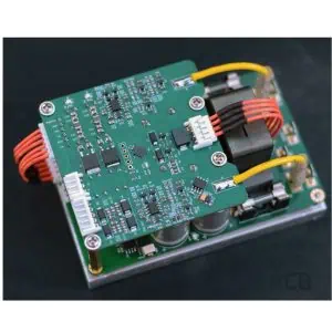
Our 10-layer PCB production service delivers precision-engineered multilayer circuits designed for demanding applications in telecommunications, aerospace, medical devices, and high-speed computing systems. With decade-proven expertise in complex PCB fabrication, we transform your most challenging designs into reliable, high-performance circuit boards.
Key Features
Superior Layer Construction
- 10 copper layers with optimized impedance control
- Ultra-thin dielectric materials for signal integrity
- Controlled layer stackup for minimal crosstalk
- Sequential lamination process ensuring perfect layer alignment
Advanced Manufacturing Capabilities
- Minimum trace width: 0.075mm (3 mil)
- Via drilling precision: ±0.025mm tolerance
- Aspect ratio support up to 12:1
- HDI (High Density Interconnect) technology available
- Blind and buried vias for space optimization
Premium Materials & Finishes
- FR-4 high-Tg materials for thermal stability
- Rogers and Isola specialty substrates available
- Multiple surface finishes: HASL, ENIG, OSP, Immersion Silver
- RoHS compliant materials and processes
Technical Specifications
Physical Parameters
- Board thickness: 1.6mm – 3.2mm
- Copper weight: 0.5oz – 4oz per layer
- Minimum hole size: 0.1mm
- Maximum board size: 600mm × 500mm
- Layer count: 10 layers standard (up to 32 layers available)
Electrical Performance
- Impedance tolerance: ±5% (±10% standard)
- Insulation resistance: >10^8 MΩ
- Dielectric withstanding voltage: 500V AC
- Thermal shock resistance: 288°C for 10 seconds
Quality Assurance
Every 10-layer PCB undergoes rigorous testing protocols including electrical testing, impedance verification, microsection analysis, and automated optical inspection. Our ISO 9001:2015 certified facility maintains strict quality standards with 99.5% first-pass yield rates.
Applications
High-Speed Digital Systems
- Server motherboards and networking equipment
- Graphics cards and high-performance computing
- 5G telecommunications infrastructure
Mission-Critical Electronics
- Aerospace avionics and defense systems
- Medical imaging and diagnostic equipment
- Industrial automation and control systems
Advanced Consumer Electronics
- Smartphones and tablets with complex RF circuits
- Automotive infotainment and ADAS systems
- IoT devices requiring miniaturization
Production Timeline
- Standard lead time: 10-15 business days
- Expedited service: 7-10 business days available
- Prototype quantities: 5-100 pieces
- Production volumes: 100-10,000+ pieces
Design Support Services
Our experienced engineering team provides comprehensive design for manufacturing (DFM) analysis, impedance calculations, and stackup optimization to ensure your 10-layer PCB meets all performance requirements while maintaining cost-effectiveness.
Get Started Today Upload your Gerber files for instant quote or contact our technical team for design consultation. We’re committed to delivering exceptional multilayer PCBs that power tomorrow’s innovations.