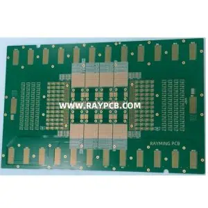
Layer : 8 Layer PCB
Thickness: 1.7mm
Copper: 1oz
Solder mask: Blue
Legend: White
Panel Size: 210*310mm /4up
Estimate PCB Cost, Pls send PCB File and Bom List to Sales@raypcb.com with Requirement.
8 Layer PCB Stackup Design and Manufacturing Cost
Introduction
In the world of electronic design, the complexity of printed circuit boards (PCBs) continues to increase as devices become more sophisticated and compact. An 8-layer PCB stackup is a popular choice for many advanced applications, offering a balance between complexity and cost-effectiveness. This article will delve into the intricacies of designing an 8-layer PCB stackup and explore the factors that influence its manufacturing cost.
Understanding 8 Layer PCB Stackups
What is a PCB Stackup?
A PCB stackup refers to the arrangement of copper layers and insulating materials that make up a multi-layer printed circuit board. The stackup design is crucial as it affects the board’s electrical performance, thermal management, and overall reliability.
Benefits of 8 Layer PCBs
8-layer PCBs offer several advantages over simpler designs:
- Increased routing density
- Better signal integrity
- Improved EMI/EMC performance
- Enhanced power distribution
- Flexibility in design choices
Designing an 8 Layer PCB Stackup
Typical Layer Configurations
When designing an 8-layer PCB stackup, there are several common configurations to consider. Here’s a table outlining some popular options:
| Layer | Configuration 1 | Configuration 2 | Configuration 3 |
|---|---|---|---|
| 1 | Signal | Signal | Signal |
| 2 | Ground | Power | Ground |
| 3 | Signal | Signal | Signal |
| 4 | Power | Ground | Power |
| 5 | Power | Ground | Power |
| 6 | Signal | Signal | Signal |
| 7 | Ground | Power | Ground |
| 8 | Signal | Signal | Signal |
Key Considerations in Stackup Design
Impedance Control
Maintaining consistent impedance throughout the board is crucial for signal integrity. Factors affecting impedance include:
- Trace width
- Dielectric thickness
- Dielectric constant of the material
Power and Ground Plane Placement
Proper placement of power and ground planes is essential for:
- Minimizing noise
- Reducing EMI
- Ensuring adequate power distribution
Signal Layer Pairing
Pairing signal layers with adjacent ground planes helps to:
- Improve signal integrity
- Reduce crosstalk
- Enhance EMI performance
Material Selection
Choosing the right materials for your 8-layer PCB is crucial. Consider factors such as:
- Dielectric constant (Dk)
- Dissipation factor (Df)
- Thermal performance
- Cost
Manufacturing Cost Factors
Material Costs
The choice of materials significantly impacts the overall cost of an 8-layer PCB. Here’s a comparison of some common materials:
| Material | Relative Cost | Dk | Df |
|---|---|---|---|
| FR-4 | Low | 4.3 | 0.020 |
| Isola 370HR | Medium | 4.1 | 0.014 |
| Rogers 4350B | High | 3.48 | 0.0037 |
Manufacturing Process Complexity
The complexity of the manufacturing process affects the cost. Factors include:
- Layer count
- Minimum trace width and spacing
- Via types (through-hole, blind, buried)
- Surface finish
Volume and Quantity
Production volume significantly impacts per-unit cost. Here’s a general cost trend:
| Quantity | Relative Cost per Unit |
|---|---|
| Prototype (1-10) | Very High |
| Small Run (11-100) | High |
| Medium Run (101-1000) | Medium |
| Large Run (1000+) | Low |
Special Requirements
Additional requirements can increase costs:
- Controlled impedance
- Tight tolerances
- Special testing (e.g., electrical test, x-ray inspection)
- Certifications (e.g., UL, RoHS)
Cost Reduction Strategies
Design for Manufacturability (DFM)
Implementing DFM principles can help reduce costs:
- Use standard trace widths and spacings
- Minimize the use of blind and buried vias
- Choose common materials and surface finishes
Optimize Layer Count
Ensure that 8 layers are necessary for your design. Sometimes, clever routing can allow for fewer layers, reducing cost.
Consider Panelization
Maximizing the number of boards per panel can significantly reduce per-unit costs, especially for smaller boards.
Balance Performance and Cost
Choose materials and manufacturing processes that meet your performance requirements without overengineering.
Conclusion
Designing an 8-layer PCB stackup requires careful consideration of electrical performance, manufacturability, and cost factors. By understanding the key design principles and cost drivers, engineers can create efficient and cost-effective designs that meet the demanding requirements of modern electronic devices.
Frequently Asked Questions (FAQ)
- Q: Why choose an 8-layer PCB over a 6-layer or 10-layer design? A: An 8-layer PCB offers a good balance between complexity and cost. It provides more routing flexibility and better signal integrity than a 6-layer board, while being less expensive than a 10-layer design. It’s often suitable for complex designs that don’t quite need the additional layers of a 10-layer board.
- Q: How does the choice of material affect the performance and cost of an 8-layer PCB? A: Material choice significantly impacts both performance and cost. High-performance materials like Rogers 4350B offer better electrical properties (lower Dk and Df) but are more expensive. Standard FR-4 is more economical but may not meet the requirements for high-speed or high-frequency applications. The material choice should be based on the specific needs of your design and budget constraints.
- Q: What are the most common challenges in designing an 8-layer PCB stackup? A: Common challenges include maintaining consistent impedance control, managing signal integrity across layers, effectively distributing power, and minimizing EMI/EMC issues. Balancing these factors while keeping the design manufacturable and cost-effective can be complex.
- Q: How can I reduce the cost of manufacturing my 8-layer PCB without compromising performance? A: Cost reduction strategies include optimizing the design for manufacturability, choosing standard materials and processes where possible, maximizing panel utilization, and ordering in larger quantities if feasible. It’s also important to ensure that an 8-layer design is truly necessary, as sometimes clever routing can allow for fewer layers.
- Q: Are there any special considerations for high-speed designs on an 8-layer PCB? A: Yes, high-speed designs require careful attention to signal integrity. This includes proper stackup design with adequate ground and power planes, controlled impedance routing, minimizing crosstalk through proper layer pairing and routing techniques, and potentially using higher-performance materials with lower Dk and Df values. Additionally, careful via design and placement become more critical in high-speed applications.