XC7K410T-2FFG900I Xilinx Kintex-7 FPGA – Datasheet, Pinout & Design Resources

Introduction

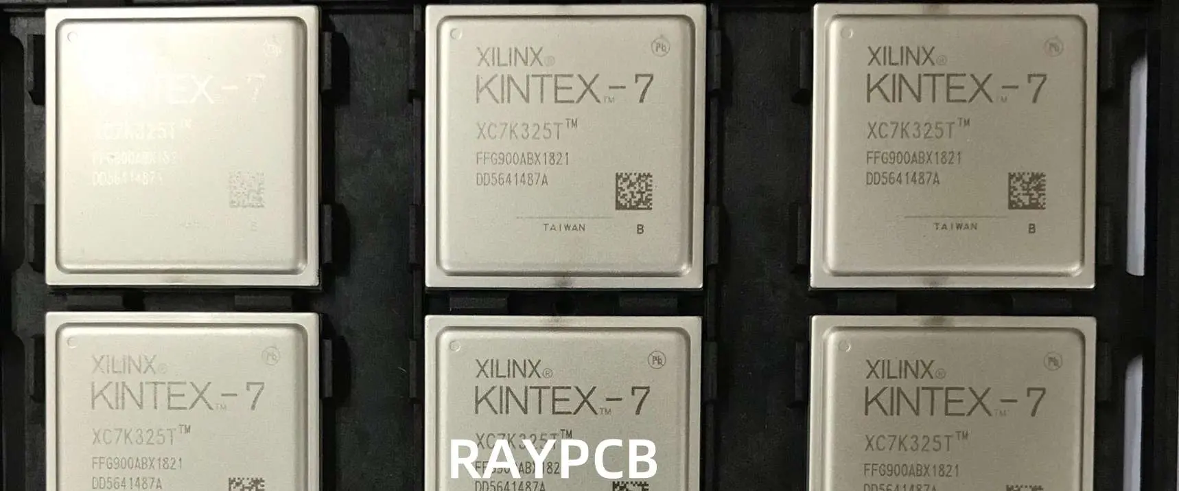
The XC7K410T-2FFG900I is a high-performance Field-Programmable Gate Array (FPGA) from Xilinx’s Kintex-7 family. This powerful device offers a blend of performance, power efficiency, and versatility, making it an excellent choice for a wide range of applications in telecommunications, data centers, medical imaging, and more. In this comprehensive guide, we’ll explore the features, specifications, and design resources available for the XC7K410T-2FFG900I, providing valuable insights for engineers and developers working with this advanced FPGA.

XC7K410T-2FFG900I: An Overview

Key Features of the Kintex-7 FPGA

The XC7K410T-2FFG900I is part of the Kintex-7 family, known for its balance of performance and cost-effectiveness. Some standout features include:

  1. High-performance DSP slices
  2. Advanced memory interface solutions
  3. High-speed serial connectivity
  4. Low power consumption
  5. Partial reconfiguration capabilities

XC7K410T-2FFG900I Specifications

Let’s delve into the specific specifications of the XC7K410T-2FFG900I:

  • Logic Cells: 406,720
  • CLB Flip-Flops: 508,400
  • CLB LUTs: 254,200
  • Maximum Distributed RAM (Kb): 5,663
  • Block RAM/FIFO (Kb): 28,620
  • DSP Slices: 1,540
  • CMTs (Mixed-Mode Clock Managers): 10
  • Maximum User I/O: 500
  • Maximum HP I/O Banks: 17
  • Maximum HR I/O Banks: 5
  • Package: FFG900 (31 x 31 mm)
  • Speed Grade: -2

These specifications highlight the device’s substantial resources, making it suitable for complex, high-performance designs.

Datasheet Analysis

DC and Switching Characteristics

The XC7K410T-2FFG900I datasheet provides detailed information on DC and switching characteristics. Key parameters include:

  • Supply Voltages:
    • VCCINT: 1.0V (Core voltage)
    • VCCAUX: 1.8V (Auxiliary voltage)
    • VCCO: 1.2V to 3.3V (I/O voltage, bank-specific)
  • Power Consumption:
    • Static power consumption varies based on design and configuration
    • Dynamic power consumption depends on resource utilization and switching frequency
  • Timing Characteristics:
    • Minimum clock period: 2.564 ns (390 MHz)
    • Setup time: 0.13 ns (typical)
    • Hold time: 0.17 ns (typical)

Environmental Specifications

The XC7K410T-2FFG900I is designed to operate reliably under various conditions:

  • Operating Temperature Range:
    • Commercial (C-grade): 0ยฐC to +85ยฐC
    • Industrial (I-grade): -40ยฐC to +100ยฐC
  • Storage Temperature Range: -65ยฐC to +150ยฐC
  • Relative Humidity: 5% to 95% (non-condensing)

Pinout and Package Information

Xilinx Kintex-7 FPGA price

FFG900 Package Overview

The XC7K410T-2FFG900I comes in a Flip-Chip Fine-Pitch Ball Grid Array (FFG) package with 900 pins. This package offers:

  • High pin count for extensive I/O capabilities
  • Excellent thermal performance
  • Compact footprint (31 x 31 mm)

Pin Categories

The pins of the XC7K410T-2FFG900I are categorized into several groups:

  1. User I/O pins
  2. Configuration pins
  3. Power supply pins (VCCINT, VCCAUX, VCCO)
  4. Ground pins
  5. JTAG interface pins
  6. MGT (Multi-Gigabit Transceiver) pins

I/O Banking Structure

The XC7K410T-2FFG900I features a flexible I/O banking structure:

  • 17 High-Performance (HP) I/O banks
  • 5 High-Range (HR) I/O banks

Each bank can be configured with different I/O standards, allowing for versatile interfacing with various external devices.

Design Resources for XC7K410T-2FFG900I

Xilinx Vivado Design Suite

The primary design tool for the XC7K410T-2FFG900I is Xilinx Vivado Design Suite. Key features include:

  • RTL-to-bitstream design flow
  • High-level synthesis capabilities
  • Advanced timing analysis and optimization
  • Power analysis and optimization tools
  • Integrated simulation environment

IP Cores and Reference Designs

Xilinx provides a rich ecosystem of IP cores and reference designs compatible with the XC7K410T-2FFG900I:

  1. DSP IP cores (FFT, FIR filters, etc.)
  2. Memory interface solutions (DDR3/DDR4 controllers)
  3. PCIe interface cores
  4. Ethernet MAC and PHY solutions
  5. Video processing IP

These resources significantly accelerate development time and reduce design risks.

Documentation and Support

Comprehensive documentation is available for the XC7K410T-2FFG900I, including:

  • Product datasheets
  • User guides
  • Application notes
  • Errata documents
  • White papers on specific design techniques

Xilinx also offers technical support through their website, forums, and direct customer support channels.

Read more about:

Application Areas

The XC7K410T-2FFG900I is well-suited for a variety of applications, including:

Telecommunications Infrastructure

  • 5G base stations
  • Network switches and routers
  • Software-defined networking (SDN) equipment

Data Center and Cloud Computing

  • High-performance computing (HPC) accelerators
  • Network interface cards (NICs)
  • Storage system controllers

Medical Imaging

  • MRI and CT scan image processing
  • Ultrasound systems
  • Digital X-ray equipment

Industrial Automation

  • Industrial vision systems
  • Robotics controllers
  • High-speed data acquisition systems

Aerospace and Defense

  • Radar signal processing
  • Electronic warfare systems
  • Satellite communication equipment

Performance Optimization Techniques

To get the most out of the XC7K410T-2FFG900I, consider the following optimization techniques:

Efficient Use of DSP Slices

The 1,540 DSP slices in the XC7K410T-2FFG900I are powerful resources for implementing arithmetic operations. To optimize their use:

  1. Leverage DSP inference in your HDL code
  2. Use Xilinx DSP IP cores for complex operations
  3. Pipeline DSP-heavy designs for higher throughput

Memory Optimization

With 28,620 Kb of Block RAM, efficient memory usage is crucial:

  1. Use appropriate memory structures (distributed RAM vs. Block RAM)
  2. Implement memory partitioning for parallel access
  3. Utilize Xilinx Memory Interface Generator (MIG) for external memory interfaces

Clock Domain Management

Proper clock domain management is essential for high-performance designs:

  1. Use Mixed-Mode Clock Managers (MMCMs) for flexible clock generation
  2. Implement proper clock domain crossing (CDC) techniques
  3. Utilize clock gating for power optimization

I/O Planning and Optimization

With 500 user I/O pins, careful I/O planning is necessary:

  1. Group related signals in the same I/O bank
  2. Use appropriate I/O standards for each interface
  3. Implement proper termination schemes for high-speed interfaces

Power Management Strategies

The XC7K410T-2FFG900I offers several power management features:

Dynamic Power Reduction

  1. Clock gating unused portions of the design
  2. Implementing power-efficient coding practices
  3. Utilizing power-optimized IP cores

Static Power Reduction

  1. Using power gating techniques for unused blocks
  2. Implementing partial reconfiguration to time-share resources
  3. Optimizing device configuration for power efficiency

Debugging and Verification

Integrated Logic Analyzer (ILA)

The Xilinx Integrated Logic Analyzer (ILA) is a powerful tool for on-chip debugging:

  1. Real-time signal monitoring
  2. Trigger-based data capture
  3. Integration with Vivado debug features

JTAG-based Debugging

The JTAG interface provides access to various debugging features:

  1. Boundary scan testing
  2. In-system programming
  3. Readback and verification of configuration data

Simulation and Verification

Xilinx provides comprehensive simulation and verification tools:

  1. Mixed-language simulation support (VHDL, Verilog, SystemVerilog)
  2. Integration with third-party simulators
  3. Formal verification tools for critical design components

Conclusion

The XC7K410T-2FFG900I Xilinx Kintex-7 FPGA is a powerful and versatile device suitable for a wide range of high-performance applications. With its extensive logic resources, high-speed I/O capabilities, and advanced features like partial reconfiguration, it offers engineers and developers a robust platform for implementing complex digital systems.

By leveraging the comprehensive design resources provided by Xilinx, including the Vivado Design Suite, IP cores, and reference designs, developers can efficiently create optimized solutions for their specific application requirements. The device’s balance of performance and power efficiency makes it an excellent choice for applications in telecommunications, data centers, medical imaging, and more.

As FPGA technology continues to evolve, the XC7K410T-2FFG900I remains a strong contender in the mid-range FPGA market, offering a compelling combination of features, performance, and cost-effectiveness. Whether you’re designing a high-speed signal processing system, a complex network interface, or an advanced medical imaging device, the XC7K410T-2FFG900I provides the resources and capabilities to bring your innovative ideas to life.

XC95144XL-10TQG100C Xilinx CPLD: Datasheet, Pinout & Features Explained

Introduction

The XC95144XL-10TQG100C is a Complex Programmable Logic Device (CPLD) manufactured by Xilinx, a leader in the field of programmable logic devices. This article provides a comprehensive overview of the device, including its key features, pinout details, and an explanation of its datasheet. Whether you’re an engineer considering this CPLD for your next project or a student learning about programmable logic, this guide will help you understand the capabilities and specifications of the XC95144XL-10TQG100C.

Overview of the XC95144XL-10TQG100C

The XC95144XL-10TQG100C is part of Xilinx’s XC9500XL family of CPLDs. It offers a balance of high performance, low power consumption, and a rich set of features, making it suitable for a wide range of applications in digital systems design.

Key Specifications:

  • Logic Cells: 144
  • Macrocells: 144
  • I/O Pins: 81
  • Package: TQFP-100 (TQG100)
  • Speed Grade: -10 (10 ns pin-to-pin delay)
  • Operating Voltage: 3.3V

Datasheet Analysis

The datasheet for the XC95144XL-10TQG100C provides detailed information about the device’s specifications, performance characteristics, and operating conditions. Let’s break down some of the key sections:

Absolute Maximum Ratings

This section outlines the extreme limits beyond which damage to the device may occur. Key parameters include:

  • Storage Temperature: -65ยฐC to +150ยฐC
  • Ambient Temperature: -40ยฐC to +85ยฐC
  • Supply Voltage (Vccint): -0.5V to +4.0V
  • Supply Voltage (Vccio): -0.5V to +4.0V

It’s crucial to note that these are absolute maximum ratings, and the device should be operated within the recommended operating conditions for reliable performance.

Recommended Operating Conditions

These conditions specify the ranges within which the device is guaranteed to function correctly:

  • Supply Voltage (Vccint): 3.3V ยฑ5%
  • Supply Voltage (Vccio): 3.3V ยฑ5%
  • Operating Temperature: 0ยฐC to +70ยฐC (Commercial) or -40ยฐC to +85ยฐC (Industrial)
  • Input Voltage: 0V to Vccio

DC Characteristics

This section provides information about the device’s electrical characteristics under static conditions. Key parameters include:

  • Input Leakage Current (IIL/IIH): ยฑ10 ยตA max
  • Output High Voltage (VOH): 2.4V min
  • Output Low Voltage (VOL): 0.4V max
  • Quiescent Supply Current (ICCQ): 100 ยตA typ, 500 ยตA max

AC Characteristics

AC characteristics describe the device’s dynamic performance. For the XC95144XL-10TQG100C, key timing parameters include:

  • Pin-to-pin delay (tPD): 10 ns max
  • Clock to Output (tCO): 6.5 ns max
  • Setup Time (tSU): 5.0 ns min
  • Hold Time (tH): 0 ns min
  • Maximum Clock Frequency (fMAX): 178 MHz

These timing parameters are crucial for ensuring proper operation in high-speed digital systems.

Read more about:

Pinout and Package Information

The XC95144XL-10TQG100C comes in a TQFP-100 package, which stands for Thin Quad Flat Pack with 100 pins. Understanding the pinout is essential for proper PCB design and interfacing with other components.

Pin Configuration:

  • Total Pins: 100
  • User I/O Pins: 81
  • Dedicated Input Pins: 3 (including global clock)
  • Power Pins (Vccint): 4
  • Power Pins (Vccio): 4
  • Ground Pins: 8

Key Pin Functions:

  1. User I/O (Pin 1-81): These pins can be configured as inputs, outputs, or bidirectional pins based on the programmed logic.
  2. GCK1, GCK2, GCK3 (Pins 91, 93, 95): Global clock inputs, which can be used to distribute clock signals throughout the device with minimal skew.
  3. TCK, TMS, TDI, TDO (Pins 88, 87, 89, 90): JTAG interface pins for programming and debugging.
  4. Vccint (Pins 14, 39, 64, 86): Core voltage supply pins (3.3V).
  5. Vccio (Pins 20, 45, 70, 96): I/O bank voltage supply pins (3.3V).
  6. GND (Pins 7, 32, 57, 82, 21, 46, 71, 97): Ground pins.

When designing a PCB layout, it’s crucial to place decoupling capacitors close to the Vccint and Vccio pins to ensure stable power supply and reduce noise.

Features Explained

The XC95144XL-10TQG100C offers a range of features that make it a versatile choice for many applications. Let’s explore some of these key features in detail:

1. FastCONNECT II Architecture

The XC95144XL uses Xilinx’s FastCONNECT II architecture, which provides a balance between speed and routability. This architecture includes:

  • 144 macrocells organized into 9 function blocks
  • High-speed, low-power CMOS technology
  • Predictable pin-to-pin delays

The FastCONNECT II switch matrix allows any function block to drive any I/O pin, providing excellent flexibility in design.

2. In-System Programmability (ISP)

The device supports in-system programmability, allowing for:

  • Programming and reprogramming directly in the target system
  • Easy design updates and field upgrades
  • Reduced time-to-market and development costs

ISP is achieved through the JTAG (IEEE 1149.1) interface, which uses the TCK, TMS, TDI, and TDO pins.

3. Power Management

The XC95144XL incorporates several power management features:

  • Low static power consumption
  • Programmable ground pin on unused I/Os
  • Sleep mode for further power reduction

These features make the device suitable for power-sensitive applications.

4. I/O Features

The I/O pins of the XC95144XL offer several advanced features:

  • Programmable slew rate control
  • Optional pull-up resistors
  • Hot-swap capability
  • 3.3V to 5V tolerant inputs

These features provide flexibility in interfacing with various other devices and standards.

5. Security

To protect intellectual property, the XC95144XL includes:

  • User-programmable security bit
  • Permanent read protection option

Once enabled, these features prevent unauthorized reading or copying of the device configuration.

6. Wide Operating Conditions

The device is designed to operate reliably across a wide range of conditions:

  • Commercial (0ยฐC to +70ยฐC) and industrial (-40ยฐC to +85ยฐC) temperature ranges
  • 3.3V core and I/O voltage

This flexibility makes the XC95144XL suitable for various environmental conditions and applications.

Application Areas

The XC95144XL-10TQG100C is versatile and can be used in a wide range of applications, including:

  1. Glue Logic: Interfacing between different digital components or bus standards.
  2. State Machines: Implementing complex control logic and sequencing operations.
  3. Address Decoding: Managing memory and peripheral addressing in microprocessor systems.
  4. Protocol Bridging: Translating between different communication protocols.
  5. I/O Expansion: Extending the I/O capabilities of microcontrollers or processors.
  6. High-Speed Control Systems: Implementing fast control loops in industrial automation.

Programming and Development

To program the XC95144XL-10TQG100C, you’ll need:

  1. Xilinx ISE WebPACK: Free software for designing with Xilinx CPLDs.
  2. JTAG Programmer: Hardware to connect your computer to the CPLD for programming.

The development process typically involves:

  1. Describing the desired logic in VHDL or Verilog
  2. Synthesizing the design
  3. Fitting the design to the CPLD architecture
  4. Generating a programming file
  5. Downloading the configuration to the device through the JTAG interface

Comparison with Other Xilinx CPLDs

The XC95144XL-10TQG100C sits in the middle of Xilinx’s XC9500XL family. Here’s how it compares to some other devices in the lineup:

DeviceLogic CellsMacrocellsUser I/OsMax. Frequency
XC9536XL363634222 MHz
XC9572XL727252208 MHz
XC95144XL14414481178 MHz
XC95288XL288288192166 MHz

The XC95144XL offers a good balance of resources and performance, making it suitable for medium-sized designs that require more logic than the smaller devices but don’t need the extensive resources of the larger ones.

Conclusion

The XC95144XL-10TQG100C is a versatile and powerful CPLD that offers a good balance of performance, power efficiency, and features. Its 144 macrocells, 81 user I/O pins, and fast pin-to-pin delays make it suitable for a wide range of digital design applications.

Key advantages include:

  • In-System Programmability for easy updates
  • Low power consumption with sleep mode
  • Flexible I/O features for easy integration
  • Robust security options to protect designs

When considering the XC95144XL-10TQG100C for your project, be sure to carefully review the datasheet and consider factors such as logic resource requirements, I/O count, speed requirements, and power constraints. With its combination of features and performance, this CPLD can be an excellent choice for many medium-complexity digital designs.

As with any complex electronic component, proper PCB design practices, including careful attention to power supply decoupling and signal integrity, are crucial for achieving optimal performance from the XC95144XL-10TQG100C.

How To Compare XC7Z020-1CLG400I With Other FPGAs?

Xilinx Artix 7

XC7Z020-1CLG400I is a highly sophisticated Field Programmable Gate Array. That’s why it is revolutionizing the way we approach complex computing tasks.  It times to discover the unique features and capabilities of this powerful device.   

The globe of electronics is evolving at a rapid pace. Every day there is innovative technology emerging all the time. One such technology that has been making waves in recent years is FPGAs. These FPGAs have revolutionized the way we approach complex computing tasks. These offer unparalleled performance and flexibility.

Although there are several FPGAs, XC7Z020-1CLG400I is an up-to-date device. It can tackle even the most demanding computing tasks. In this article, we’ll take a closer look at what the XC7Z020-1CLG400I is. How can you compare with other FPGAs? What are the key factors for comparison?

 What Is XC7Z020-1CLG400I?

 The XC7Z020-1CLG400I is a type of FPGA. FPGAs are field Programmable Gate Arrays that can perform specific computing tasks. XC7Z020-1CLG400I FPGAs are highly flexible. You can reconfigure them easily.

The XC7Z020-1CLG400I is a highly advanced FPGA due to its exceptional performance and flexibility. This powerful FPGA is a part of the Zynq-7000 family of FPGAs. They are some of the most superior FPGAs on the market today.

Features Of XC7Z020-1CLG400I

The XC7Z020-1CLG400I is a highly versatile device that offers a range of features and capabilities that make it an ideal choice for a wide range of computing applications. Some of the key features of this powerful FPGA include

  • It has dual-core ARM Cortex-A9 processors
  • Up to 85,000 logic cells as building blocks
  • Two hundred twenty DSP slices is a wonderful feature
  • One GB DDR3 SDRAM
  • High-speed serial connectivity
  • Programmable I/Os
  • 10/100/1000 Ethernet MAC
  • PCI Express Gen 2

How Does Xc7z020-1clg400i Work?

The XC7Z020-1CLG400I functions by enabling users to program the device to execute specific computational operations. It utilizes the hardware description language (HDL) such as Verilog or VHDL. Upon completion of programming, the device can execute the computational tasks. Since FPGAs are exceptionally adaptable, the programming is modified by accommodating or shifting computational demands. The XC7Z020-1CLG400I’s dual-core ARM Cortex-A9 processors are a significant benefit, as they offer remarkable performance and efficiency. In addition, it is an optimal choice for strenuous computational applications.

Key Factors To Keep In Mind While Comparing XC7Z020-1CLG400I With Other FPGA

FULL PCB MANUFACTURING Quote

 Sometimes it’s necessary to compare different FPGAs to choose the right one. If you choose the wrong FPGA, it will destroy the whole concept. That s why it is necessary to keep certain apartments in mind.

When it comes to comparing the XC7Z020-1CLG400I with other FPGAs on the market, the following are the key factors to look at.

1. Performance

 Performance is the main key factor. Do you know why designers and engineers go for XC7Z020-1CLG400I? It is exceptional in its exceptional performance and processing speed. With up to 85,000 logic cells and 220 DSP slices, this powerful FPGA is just amazing. That’s why it can easily handle even the most demanding computing tasks. When compared to other FPGAs on the market, the XC7Z020-1CLG400I often comes out ahead in terms of performance. Still, there are some FPGAs that are great or even better performance. That’s why some people get confused. As a result, they decide or choose the wrong one. But XC7Z020-1CLG400I is one of the top-performing FPGAs available today. In addition, it offers great processing performance in all aspects.

2. Flexibility For Customization

How flexible are your FPGAs as compared to other FPGAs? This is an important factor when making a comparison. The XC7Z020-1CLG400I offers great flexibility. All FPGAs are reconfigured easily but every FPGA has limitations in reconfiguring. They also have reconfiguring capacity. XC7Z020-1CLG400I offers a great level of flexibility that traditional 

FPGAs and integrated circuits simply can’t match. You compare it with other FPGAs, the XC7Z020-1CLG400I shows greater reconfiguring capacity. That’s why it is an ideal choice for applications where flexibility is key. For example, industrial automation and communications have the best place for this FPGA. That’s why it is necessary to focus on the flexibility of both the FPGA. Always go for the better flexibility FPGA. Flexibility for reconfiguring is the must option to compare. You have to recognize FPGA several times during work.

3. The Need And Requirements

ย All FPGAs are not equal. Every FPGA has up and downsides. That’s why a detailed comparison is necessary. Moreover, when comparing XC7Z020-1CLG400I with other FPGAs, then must keep in mind your need and requirements. XC7Z020-1CLG400I FPGA mostly fulfills the demand of designers. If you choose an FPGA that doesn’t meet the needs, then you will lose the game. As a result, you cannot achieve desired outcomes. That’s why it is important to compare your selected FPGA and some available FPGAs for better results.

4. Price Comparison

 Price is the last key factor. Yes, price matters, but FPGA’s qualities also matter. No doubt price is always an important factor to consider but keep in mind your need also. What do you expect from FPGA? Sometimes you choose FPGA that doesn’t suit your need. As a result, you are unable to achieve your objectives. While the XC7Z020-1CLG400I is certainly a powerful and versatile FPGA but it is on the higher price side. Some people don’t like it due to its price, and they go for cheaper options having similar properties.

However, for applications where performance and flexibility are a top priority, the XC7Z020-1CLG400I is ideal. That’s why don’t compromise quality features over price.

 Wrapping Up the Things

Overall, the XC7Z020-1CLG400I is a modern and versatile FPGA. That’s why it offers exceptional performance and flexibility. It is more expensive than some other FPGAs on the market. But its unique features make it an ideal choice for a wide range of computing applications.

When you compare it with other FPGAs, the XC7Z020-1CLG400I often comes first. Because its performance and flexibility are superb, it’s important to carefully consider your specific needs before purchasing. Above all, XC7Z020-1CLG400I FPGA is useful for many needs and comparatively better for different tasks.

Xilinx XC2C32A-6CP56I -Internet of Things -Medical Equipment

Xilinx XC2C32A-6CP56I ApplicationField

-Artificial Intelligence
-Cloud Computing
-5G Technology
-Industrial Control
-Wireless Technology
-Medical Equipment
-Consumer Electronics
-Internet of Things

Request Xilinx XC2C32A-6CP56I FPGA Quote, Pls Send Email to Sales@raypcb.com Now

Xilinx XC2C32A-6CP56I FAQ

Q: How to obtain XC2C32A-6CP56I technical support documents?
A: Enter the “XC2C32A-6CP56I” keyword in the search box of the website, or find these through the Download Channel or FPGA Forum .

Q: Do I have to sign up on the website to make an inquiry for XC2C32A-6CP56I?
A: No, only submit the quantity, email address and other contact information required for the inquiry of XC2C32A-6CP56I, but you need to sign up for the post comments and resource downloads.

Q: How can I obtain software development tools related to the Xilinx FPGA platform?
A: In FPGA/CPLD design tools, Xilinx’s Vivado Design Suite is easy to use, it is very user-friendly in synthesis and implementation, and it is easier to use than ISE design tools; The specific choice depends on personal habits and functional requirements to specifically select a more suitable match. You can search and download through the FPGA resource channel.

Q: Does the price of XC2C32A-6CP56I devices fluctuate frequently?
A: The RAYPCB search engine monitors the XC2C32A-6CP56I inventory quantity and price of global electronic component suppliers in real time, and regularly records historical price data. You can view the historical price trends of electronic components to provide a basis for your purchasing decisions.

Q: Where can I purchase Xilinx XC2C32A Development Boards, Evaluation Boards, or CoolRunner-II CPLD Starter Kit? also provide technical information?
A: RAYPCB does not provide development board purchase services for the time being, but customers often consult about ZedBoard, Basys 3 board, TinyFPGA BX, Nexys4-DDR, Terasic DE10-Nano, Digilent Arty S7, etc. If you need relevant technical information, you can submit feedback information, our technicians will contact you soon.

Q: What should I do if I did not receive the technical support for XC2C32A6CP56I in time?
A: Depending on the time difference between your location and our location, it may take several hours for us to reply, please be patient, our FPGA technical engineer will help you with the XC2C32A-6CP56I pinout information, replacement, datasheet in pdf, programming tools, starter kit, etc.

Xilinx XC2C32A-6CP56I Features

• In-System Programmable PROMs for Configuration of Xilinx FPGAs

Request Xilinx XC2C32A-6CP56I FPGA Quote, Pls Send Email to Sales@raypcb.com Now

Xilinx XC2C32A-6CP56I Overview

This XC2C32A-6CP56I device consists of eight Function Blocks inter-connected by a low power Advanced Interconnect Matrix (AIM). The AIM feeds 40 true and complement inputs to each Function Block. The Function Blocks consist of a 40 by 56 P-term PLA and 16 macrocells which contain numerous configuration bits that allow for combinational or registered modes of operation.Additionally, these registers can be globally reset or preset and configured as a D or T flip-flop or as a D latch. There are also multiple clock signals, both global and local product term types, configured on a per macrocell basis. Output pin configurations include slew rate limit, bus hold, pull-up, open drain and programmable grounds. A Schmitt-trigger input is available on a per input pin basis. In addition to storing macrocell output states, the macrocell registers may be configured as direct input registers to store signals directly from input pins.Clocking is available on a global or Function Block basis. Three global clocks are available for all Function Blocks as a synchronous clock source. Macrocell registers can be individually configured to power up to the zero or one state. A global set/reset control line is also available to asynchronously set or reset selected registers during operation. Additional local clock, synchronous clock-enable, asynchronous set/reset and output enable signals can be formed using product terms on a per-macrocell or per-Function Block basis.A DualEDGE flip-flop feature is also available on a per macrocell basis. This feature allows high performance synchronous operation based on lower frequency clocking to help reduce the total power consumption of the device.Circuitry has also been included to divide one externally supplied global clock (GCK2) by eight different selections. This yields divide by even and odd clock frequencies.The XC2C32A-6CP56I CPLD is I/O compatible with various JEDEC I/O standards (see Table 1). This XC2C32A-6CP56I device is also 1.5V I/O compatible with the use of Schmitt-trigger inputs.By mapping a signal to the DataGATE function, lower power can be achieved due to reduction in signal switching.Another feature that eases voltage translation is I/O banking. Two I/O banks are available on the CoolRunner-II 128 macrocell XC2C32A-6CP56I device that permit easy interfacing to 3.3V, 2.5V, 1.8V, and 1.5V devices.
The Xilinx CPLDs series XC2C32A-6CP56I is 32 MACROCELL 1.8V ZERO POWER ISP CPLD, View Substitutes & Alternatives along with datasheets, stock, pricing from Authorized Distributors at RAYPCB.com,
and you can also search for other FPGAs products.

Xilinx XC2C32A-6CP56I Tags

1. XC2C32A reference design
2. Xilinx CoolRunner-II CPLD development board
3. CoolRunner-II CPLD starter kit
4. XC2C32A evaluation board
5. XC2C32A development board
6. CoolRunner-II CPLD evaluation kit
7. CoolRunner-II CPLD XC2C32A
8. Xilinx XC2C32A
9. XC2C32A evaluation board

Xilinx XC2C32A-6CP56I TechnicalAttributes

-Programmable Type In System Programmable
-Number of Logic Elements/Blocks 2
-Number of I/O 33
-Number of Macrocells 32
-Number of Gates 750
-Supplier Device Package 56-CSBGA (6×6)
-Delay Time tpd(1) Max 5.5ns
-Package / Case 56-LFBGA, CSPBGA
-Operating Temperature -40โ„ƒ ~ 85โ„ƒ (TA)
-Voltage Supply – Internal 1.7V ~ 1.9V

-Mounting Type Surface Mount

Xilinx XC2C128-7VQG100C -5G Technology -Wireless Technology

Xilinx XC2C128-7VQG100C ApplicationField

-Cloud Computing
-Artificial Intelligence
-Medical Equipment
-Consumer Electronics
-Industrial Control
-Wireless Technology
-Internet of Things
-5G Technology

Request Xilinx XC2C128-7VQG100C FPGA Quote, Pls Send Email to Sales@raypcb.com Now

Xilinx XC2C128-7VQG100C FAQ

Q: How can I obtain software development tools related to the Xilinx FPGA platform?
A: In FPGA/CPLD design tools, Xilinx’s Vivado Design Suite is easy to use, it is very user-friendly in synthesis and implementation, and it is easier to use than ISE design tools; The specific choice depends on personal habits and functional requirements to specifically select a more suitable match. You can search and download through the FPGA resource channel.

Q: Does the price of XC2C128-7VQG100C devices fluctuate frequently?
A: The RAYPCB search engine monitors the XC2C128-7VQG100C inventory quantity and price of global electronic component suppliers in real time, and regularly records historical price data. You can view the historical price trends of electronic components to provide a basis for your purchasing decisions.

Q: Where can I purchase Xilinx XC2C128 Development Boards, Evaluation Boards, or CoolRunner-II CPLD Starter Kit? also provide technical information?
A: RAYPCB does not provide development board purchase services for the time being, but customers often consult about ZedBoard, Basys 3 board, TinyFPGA BX, Nexys4-DDR, Terasic DE10-Nano, Digilent Arty S7, etc. If you need relevant technical information, you can submit feedback information, our technicians will contact you soon.

Q: What should I do if I did not receive the technical support for XC2C1287VQG100C in time?
A: Depending on the time difference between your location and our location, it may take several hours for us to reply, please be patient, our FPGA technical engineer will help you with the XC2C128-7VQG100C pinout information, replacement, datasheet in pdf, programming tools, starter kit, etc.

Q: Do I have to sign up on the website to make an inquiry for XC2C128-7VQG100C?
A: No, only submit the quantity, email address and other contact information required for the inquiry of XC2C128-7VQG100C, but you need to sign up for the post comments and resource downloads.

Q: How to obtain XC2C128-7VQG100C technical support documents?
A: Enter the “XC2C128-7VQG100C” keyword in the search box of the website, or find these through the Download Channel or FPGA Forum .

Xilinx XC2C128-7VQG100C Features

• Endurance of 20,000 Program/Erase Cycles

Request Xilinx XC2C128-7VQG100C FPGA Quote, Pls Send Email to Sales@raypcb.com Now

Xilinx XC2C128-7VQG100C Overview

The CoolRunner-II 128-macrocell device is designed for both high performance and low power applications. This lends power savings to high-end communication equipment and high speed to battery operated devices. Due to the low power stand-by and dynamic operation, overall system reliability is improvedThis device consists of eight Function Blocks inter-connected by a low power Advanced Interconnect Matrix (AIM). The AIM feeds 40 true and complement inputs to each Function Block. The Function Blocks consist of a 40 by 56 P-term PLA and 16 macrocells which contain numerous configuration bits that allow for combinational or registered modes of operation.Additionally, these registers can be globally reset or preset and configured as a D or T flip-flop or as a D latch. There are also multiple clock signals, both global and local product term types, configured on a per macrocell basis. Output pin configurations include slew rate limit, bus hold, pull-up, open drain and programmable grounds. A Schmitt-trigger input is available on a per input pin basis. In addition to storing macrocell output states, the macrocell registers may be configured as direct input registers to store signals directly from input pins.Clocking is available on a global or Function Block basis. Three global clocks are available for all Function Blocks as a synchronous clock source. Macrocell registers can be individually configured to power up to the zero or one state. A global set/reset control line is also available to asynchronously set or reset selected registers during operation. Additional local clock, synchronous clock-enable, asynchronous set/reset and output enable signals can be formed using product terms on a per-macrocell or per-Function Block basis.A DualEDGE flip-flop feature is also available on a per macrocell basis. This feature allows high performance synchronous operation based on lower frequency clocking to help reduce the total power consumption of the device.Circuitry has also been included to divide one externally supplied global clock (GCK2) by eight different selections. This yields divide by even and odd clock frequencies.The use of the clock divide (division by 2) and DualEDGE flip-flop gives the resultant CoolCLOCK featureDataGATE is a method to selectively disable inputs of the CPLD that are not of interest during certain points in time.By mapping a signal to the DataGATE function, lower power can be achieved due to reduction in signal switching.Another feature that eases voltage translation is I/O banking. Two I/O banks are available on the CoolRunner-II 128 macrocell device that permit easy interfacing to 3.3V, 2.5V, 1.8V, and 1.5V devices.The CoolRunner-II 128 macrocell CPLD is I/O compatible with various JEDEC I/O standards (see Table 1). This device is also 1.5V I/O compatible with the use of Schmitt-trigger inputs.Table 1: I/O Standards for XC2C128(1)IOSTANDARD AttributeOutput VCCIOInput VCCIOInput VREFBoard Termination Voltage VTTLVTTL3.33.3N/AN/ALVCMOS333.33.3N/AN/ALVCMOS252.52.5N/AN/ALVCMOS181.81.8N/AN/ALVCMOS15(2)1.51.5N/AN/AHSTL_11.51.50.750.75SSTL2_12.52.51.251.25SSTL3_13.33.31.51.5
The Xilinx Embedded – CPLDs (Complex Programmable Logic Devices) series XC2C128-7VQG100C is CPLD CoolRunner -II Family 3K Gates 128 Macro Cells 152MHz 0.18um (CMOS) Technology 1.8V, View Substitutes & Alternatives along with datasheets, stock, pricing from Authorized Distributors at RAYPCB.com,
and you can also search for other FPGAs products.

Xilinx XC2C128-7VQG100C Tags

1. XC2C128 development board
2. Xilinx XC2C128
3. XC2C128-7VQG100C Datasheet PDF
4. CoolRunner-II CPLD XC2C128
5. CoolRunner-II CPLD evaluation kit
6. XC2C128 evaluation board
7. XC2C128 reference design
8. CoolRunner-II CPLD starter kit
9. CoolRunner-II CPLD XC2C128

Xilinx XC2C128-7VQG100C TechnicalAttributes

-Package / Case 100-TQFP
-Voltage Supply – Internal 1.7V ~ 1.9V
-Number of Gates 3000
-Number of Logic Elements/Blocks 8
-Delay Time tpd(1) Max 7.0ns
-Number of I/O 80
-Programmable Type In System Programmable
-Supplier Device Package 100-VQFP (14×14)
-Mounting Type Surface Mount
-Number of Macrocells 128

-Operating Temperature 0โ„ƒ ~ 70โ„ƒ (TA)

Xilinx XC2C256-7VQG100I -Medical Equipment -Industrial Control

Xilinx XC2C256-7VQG100I ApplicationField

-5G Technology
-Wireless Technology
-Internet of Things
-Consumer Electronics
-Cloud Computing
-Industrial Control
-Artificial Intelligence
-Medical Equipment

Request Xilinx XC2C256-7VQG100I FPGA Quote, Pls Send Email to Sales@raypcb.com Now

Xilinx XC2C256-7VQG100I FAQ

Q: How can I obtain software development tools related to the Xilinx FPGA platform?
A: In FPGA/CPLD design tools, Xilinx’s Vivado Design Suite is easy to use, it is very user-friendly in synthesis and implementation, and it is easier to use than ISE design tools; The specific choice depends on personal habits and functional requirements to specifically select a more suitable match. You can search and download through the FPGA resource channel.

Q: How to obtain XC2C256-7VQG100I technical support documents?
A: Enter the “XC2C256-7VQG100I” keyword in the search box of the website, or find these through the Download Channel or FPGA Forum .

Q: Does the price of XC2C256-7VQG100I devices fluctuate frequently?
A: The RAYPCB search engine monitors the XC2C256-7VQG100I inventory quantity and price of global electronic component suppliers in real time, and regularly records historical price data. You can view the historical price trends of electronic components to provide a basis for your purchasing decisions.

Q: What should I do if I did not receive the technical support for XC2C2567VQG100I in time?
A: Depending on the time difference between your location and our location, it may take several hours for us to reply, please be patient, our FPGA technical engineer will help you with the XC2C256-7VQG100I pinout information, replacement, datasheet in pdf, programming tools, starter kit, etc.

Q: Do I have to sign up on the website to make an inquiry for XC2C256-7VQG100I?
A: No, only submit the quantity, email address and other contact information required for the inquiry of XC2C256-7VQG100I, but you need to sign up for the post comments and resource downloads.

Q: Where can I purchase Xilinx XC2C256 Development Boards, Evaluation Boards, or CoolRunner-II CPLD Starter Kit? also provide technical information?
A: RAYPCB does not provide development board purchase services for the time being, but customers often consult about ZedBoard, Basys 3 board, TinyFPGA BX, Nexys4-DDR, Terasic DE10-Nano, Digilent Arty S7, etc. If you need relevant technical information, you can submit feedback information, our technicians will contact you soon.

Xilinx XC2C256-7VQG100I Features

– As fast as 5.7 ns pin-to-pin delays
– Optimized architecture for effective logic synthesis. Refer to the CoolRunner-II family data sheet for architecture description.
– As low as 13 μA quiescent current
– Multi-voltage I/O operation — 1.5V to 3.3V
• Available in multiple package options

• Industry’s best 0.18 micron CMOS CPLD
– Pb-free available for all packages

• Optimized for 1.8V systems
– 100-pin VQFP with 80 user I/O
– 256-ball FT (1.0mm) BGA with 184 user I/O

– 132-ball CP (0.5mm) BGA with 106 user I/O
– 144-pin TQFP with 118 user I/O

– 208-pin PQFP with 173 user I/O

Request Xilinx XC2C256-7VQG100I FPGA Quote, Pls Send Email to Sales@raypcb.com Now

Xilinx XC2C256-7VQG100I Overview

The CoolRunner-II 128 macrocell CPLD is I/O compatible with various JEDEC I/O standards (see Table 1). This XC2C256-7VQG100I device is also 1.5V I/O compatible with the use of Schmitt-trigger inputs. The XC2C256-7VQG100I device is designed for both high performance and low power applications. This lends power savings to high-end communication equipment and high speed to battery operated devices. Due to the low power stand-by and dynamic operation, overall system reliability is improved
This XC2C256-7VQG100I device consists of eight Function Blocks inter-connected by a low power Advanced Interconnect Matrix (AIM). The AIM feeds 40 true and complement inputs to each Function Block. The Function Blocks consist of a 40 by 56 P-term PLA and 16 macrocells which contain numerous configuration bits that allow for combinational or registered modes of operation.
Additionally, these registers can be globally reset or preset and configured as a D or T flip-flop or as a D latch. There are also multiple clock signals, both global and local product term types, configured on a per macrocell basis. Output pin configurations include slew rate limit, bus hold, pull-up, open drain and programmable grounds. A Schmitt-trigger input is available on a per input pin basis. In addition to storing macrocell output states, the macrocell registers may be configured as direct input registers to store signals directly from input pins.
Clocking is available on a global or Function Block basis. Three global clocks are available for all Function Blocks as a synchronous clock source. Macrocell registers can be individually configured to power up to the zero or one state. A global set/reset control line is also available to asynchronously set or reset selected registers during operation. Additional local clock, synchronous clock-enable, asynchronous set/reset and output enable signals can be formed using product terms on a per-macrocell or per-Function Block basis.
A DualEDGE flip-flop feature is also available on a per macrocell basis. This feature allows high performance synchronous operation based on lower frequency clocking to help reduce the total power consumption of the XC2C256-7VQG100I device.
Circuitry has also been included to divide one externally supplied global clock (GCK2) by eight different selections. This yields divide by even and odd clock frequencies.
The use of the clock divide (division by 2) and DualEDGE flip-flop gives the resultant CoolCLOCK feature
DataGATE is a method to selectively disable inputs of the CPLD that are not of interest during certain points in time.
By mapping a signal to the DataGATE function, lower power can be achieved due to reduction in signal switching.
Another feature that eases voltage translation is I/O banking. Two I/O banks are available on the XC2C256-7VQG100I device that permit easy interfacing to 3.3V, 2.5V, 1.8V, and 1.5V devices.
The Xilinx CPLDs series XC2C256-7VQG100I is 256 MACROCELL 1.8V ZERO POWER ISP CPLD, View Substitutes & Alternatives along with datasheets, stock, pricing from Authorized Distributors at RAYPCB.com,
and you can also search for other FPGAs products.

Xilinx XC2C256-7VQG100I Tags

1. Xilinx CoolRunner-II CPLD development board
2. XC2C256 development board
3. CoolRunner-II CPLD evaluation kit
4. Xilinx XC2C256
5. CoolRunner-II CPLD XC2C256
6. XC2C256 evaluation board
7. XC2C256-7VQG100I Datasheet PDF
8. XC2C256 reference design
9. Xilinx XC2C256

Xilinx XC2C256-7VQG100I TechnicalAttributes

-RoHS Compliant
-ECCN Code EAR99
-Product Lifecycle Status Active
-Lead-Free Status Lead Free
-HK STC License NLR

-Packaging Tray

-Mounting Style Surface Mount
-Case/Package 100-TQFP

Xilinx XC2C128-7VQ100C -Artificial Intelligence -Cloud Computing

Xilinx XC2C128-7VQ100C ApplicationField

-Wireless Technology
-Industrial Control
-Medical Equipment
-5G Technology
-Consumer Electronics
-Cloud Computing
-Internet of Things
-Artificial Intelligence

Request Xilinx XC2C128-7VQ100C FPGA Quote, Pls Send Email to Sales@raypcb.com Now

Xilinx XC2C128-7VQ100C FAQ

Q: What should I do if I did not receive the technical support for XC2C1287VQ100C in time?
A: Depending on the time difference between your location and our location, it may take several hours for us to reply, please be patient, our FPGA technical engineer will help you with the XC2C128-7VQ100C pinout information, replacement, datasheet in pdf, programming tools, starter kit, etc.

Q: Where can I purchase Xilinx XC2C128 Development Boards, Evaluation Boards, or CoolRunner-II CPLD Starter Kit? also provide technical information?
A: RAYPCB does not provide development board purchase services for the time being, but customers often consult about ZedBoard, Basys 3 board, TinyFPGA BX, Nexys4-DDR, Terasic DE10-Nano, Digilent Arty S7, etc. If you need relevant technical information, you can submit feedback information, our technicians will contact you soon.

Q: How can I obtain software development tools related to the Xilinx FPGA platform?
A: In FPGA/CPLD design tools, Xilinx’s Vivado Design Suite is easy to use, it is very user-friendly in synthesis and implementation, and it is easier to use than ISE design tools; The specific choice depends on personal habits and functional requirements to specifically select a more suitable match. You can search and download through the FPGA resource channel.

Q: How to obtain XC2C128-7VQ100C technical support documents?
A: Enter the “XC2C128-7VQ100C” keyword in the search box of the website, or find these through the Download Channel or FPGA Forum .

Q: Do I have to sign up on the website to make an inquiry for XC2C128-7VQ100C?
A: No, only submit the quantity, email address and other contact information required for the inquiry of XC2C128-7VQ100C, but you need to sign up for the post comments and resource downloads.

Q: Does the price of XC2C128-7VQ100C devices fluctuate frequently?
A: The RAYPCB search engine monitors the XC2C128-7VQ100C inventory quantity and price of global electronic component suppliers in real time, and regularly records historical price data. You can view the historical price trends of electronic components to provide a basis for your purchasing decisions.

Xilinx XC2C128-7VQ100C Features

• Endurance of 20,000 Program/Erase Cycles

Request Xilinx XC2C128-7VQ100C FPGA Quote, Pls Send Email to Sales@raypcb.com Now

Xilinx XC2C128-7VQ100C Overview

The CoolRunner-II 128-macrocell device is designed for both high performance and low power applications. This lends power savings to high-end communication equipment and high speed to battery operated devices. Due to the low power stand-by and dynamic operation, overall system reliability is improvedThis device consists of eight Function Blocks inter-connected by a low power Advanced Interconnect Matrix (AIM). The AIM feeds 40 true and complement inputs to each Function Block. The Function Blocks consist of a 40 by 56 P-term PLA and 16 macrocells which contain numerous configuration bits that allow for combinational or registered modes of operation.Additionally, these registers can be globally reset or preset and configured as a D or T flip-flop or as a D latch. There are also multiple clock signals, both global and local product term types, configured on a per macrocell basis. Output pin configurations include slew rate limit, bus hold, pull-up, open drain and programmable grounds. A Schmitt-trigger input is available on a per input pin basis. In addition to storing macrocell output states, the macrocell registers may be configured as direct input registers to store signals directly from input pins.Clocking is available on a global or Function Block basis. Three global clocks are available for all Function Blocks as a synchronous clock source. Macrocell registers can be individually configured to power up to the zero or one state. A global set/reset control line is also available to asynchronously set or reset selected registers during operation. Additional local clock, synchronous clock-enable, asynchronous set/reset and output enable signals can be formed using product terms on a per-macrocell or per-Function Block basis.A DualEDGE flip-flop feature is also available on a per macrocell basis. This feature allows high performance synchronous operation based on lower frequency clocking to help reduce the total power consumption of the device.Circuitry has also been included to divide one externally supplied global clock (GCK2) by eight different selections. This yields divide by even and odd clock frequencies.The use of the clock divide (division by 2) and DualEDGE flip-flop gives the resultant CoolCLOCK featureDataGATE is a method to selectively disable inputs of the CPLD that are not of interest during certain points in time.By mapping a signal to the DataGATE function, lower power can be achieved due to reduction in signal switching.Another feature that eases voltage translation is I/O banking. Two I/O banks are available on the CoolRunner-II 128 macrocell device that permit easy interfacing to 3.3V, 2.5V, 1.8V, and 1.5V devices.The CoolRunner-II 128 macrocell CPLD is I/O compatible with various JEDEC I/O standards (see Table 1). This device is also 1.5V I/O compatible with the use of Schmitt-trigger inputs.Table 1: I/O Standards for XC2C128(1)IOSTANDARD AttributeOutput VCCIOInput VCCIOInput VREFBoard Termination Voltage VTTLVTTL3.33.3N/AN/ALVCMOS333.33.3N/AN/ALVCMOS252.52.5N/AN/ALVCMOS181.81.8N/AN/ALVCMOS15(2)1.51.5N/AN/AHSTL_11.51.50.750.75SSTL2_12.52.51.251.25SSTL3_13.33.31.51.5
The Xilinx CPLDs series XC2C128-7VQ100C is 128 MACROCELL 1.8V ZERO POWER ISP CPLD, View Substitutes & Alternatives along with datasheets, stock, pricing from Authorized Distributors at RAYPCB.com,
and you can also search for other FPGAs products.

Xilinx XC2C128-7VQ100C Tags

1. XC2C128 reference design
2. CoolRunner-II CPLD starter kit
3. Xilinx XC2C128
4. CoolRunner-II CPLD evaluation kit
5. CoolRunner-II CPLD XC2C128
6. XC2C128 development board
7. Xilinx CoolRunner-II CPLD development board
8. XC2C128-7VQ100C Datasheet PDF
9. CoolRunner-II CPLD evaluation kit

Xilinx XC2C128-7VQ100C TechnicalAttributes

-Programmable Type In System Programmable
-Supplier Device Package 100-VQFP (14×14)
-Number of Gates 3000
-Delay Time tpd(1) Max 7.0ns
-Voltage Supply – Internal 1.7V ~ 1.9V
-Mounting Type Surface Mount
-Number of Logic Elements/Blocks 8
-Package / Case 100-TQFP
-Number of Macrocells 128
-Operating Temperature 0โ„ƒ ~ 70โ„ƒ (TA)

-Number of I/O 80

Xilinx XC2C256-7VQG100C -5G Technology -Cloud Computing

Xilinx XC2C256-7VQG100C ApplicationField

-Medical Equipment
-Wireless Technology
-Industrial Control
-Consumer Electronics
-Artificial Intelligence
-Cloud Computing
-Internet of Things
-5G Technology

Request Xilinx XC2C256-7VQG100C FPGA Quote, Pls Send Email to Sales@raypcb.com Now

Xilinx XC2C256-7VQG100C FAQ

Q: Does the price of XC2C256-7VQG100C devices fluctuate frequently?
A: The RAYPCB search engine monitors the XC2C256-7VQG100C inventory quantity and price of global electronic component suppliers in real time, and regularly records historical price data. You can view the historical price trends of electronic components to provide a basis for your purchasing decisions.

Q: Where can I purchase Xilinx XC2C256 Development Boards, Evaluation Boards, or CoolRunner-II CPLD Starter Kit? also provide technical information?
A: RAYPCB does not provide development board purchase services for the time being, but customers often consult about ZedBoard, Basys 3 board, TinyFPGA BX, Nexys4-DDR, Terasic DE10-Nano, Digilent Arty S7, etc. If you need relevant technical information, you can submit feedback information, our technicians will contact you soon.

Q: What should I do if I did not receive the technical support for XC2C2567VQG100C in time?
A: Depending on the time difference between your location and our location, it may take several hours for us to reply, please be patient, our FPGA technical engineer will help you with the XC2C256-7VQG100C pinout information, replacement, datasheet in pdf, programming tools, starter kit, etc.

Q: How can I obtain software development tools related to the Xilinx FPGA platform?
A: In FPGA/CPLD design tools, Xilinx’s Vivado Design Suite is easy to use, it is very user-friendly in synthesis and implementation, and it is easier to use than ISE design tools; The specific choice depends on personal habits and functional requirements to specifically select a more suitable match. You can search and download through the FPGA resource channel.

Q: How to obtain XC2C256-7VQG100C technical support documents?
A: Enter the “XC2C256-7VQG100C” keyword in the search box of the website, or find these through the Download Channel or FPGA Forum .

Q: Do I have to sign up on the website to make an inquiry for XC2C256-7VQG100C?
A: No, only submit the quantity, email address and other contact information required for the inquiry of XC2C256-7VQG100C, but you need to sign up for the post comments and resource downloads.

Xilinx XC2C256-7VQG100C Features

• Industry’s best 0.18 micron CMOS CPLD
– 256-ball FT (1.0mm) BGA with 184 user I/O
• Optimized for 1.8V systems
– Optimized architecture for effective logic synthesis. Refer to the CoolRunner-II family data sheet for architecture description.
– 100-pin VQFP with 80 user I/O

– As low as 13 μA quiescent current
– Pb-free available for all packages

– 208-pin PQFP with 173 user I/O
– As fast as 5.7 ns pin-to-pin delays
– Multi-voltage I/O operation — 1.5V to 3.3V

– 132-ball CP (0.5mm) BGA with 106 user I/O
• Available in multiple package options

– 144-pin TQFP with 118 user I/O

Request Xilinx XC2C256-7VQG100C FPGA Quote, Pls Send Email to Sales@raypcb.com Now

Xilinx XC2C256-7VQG100C Overview

The CoolRunner-II 128 macrocell CPLD is I/O compatible with various JEDEC I/O standards (see Table 1). This XC2C256-7VQG100C device is also 1.5V I/O compatible with the use of Schmitt-trigger inputs. The XC2C256-7VQG100C device is designed for both high performance and low power applications. This lends power savings to high-end communication equipment and high speed to battery operated devices. Due to the low power stand-by and dynamic operation, overall system reliability is improved
This XC2C256-7VQG100C device consists of eight Function Blocks inter-connected by a low power Advanced Interconnect Matrix (AIM). The AIM feeds 40 true and complement inputs to each Function Block. The Function Blocks consist of a 40 by 56 P-term PLA and 16 macrocells which contain numerous configuration bits that allow for combinational or registered modes of operation.
Additionally, these registers can be globally reset or preset and configured as a D or T flip-flop or as a D latch. There are also multiple clock signals, both global and local product term types, configured on a per macrocell basis. Output pin configurations include slew rate limit, bus hold, pull-up, open drain and programmable grounds. A Schmitt-trigger input is available on a per input pin basis. In addition to storing macrocell output states, the macrocell registers may be configured as direct input registers to store signals directly from input pins.
Clocking is available on a global or Function Block basis. Three global clocks are available for all Function Blocks as a synchronous clock source. Macrocell registers can be individually configured to power up to the zero or one state. A global set/reset control line is also available to asynchronously set or reset selected registers during operation. Additional local clock, synchronous clock-enable, asynchronous set/reset and output enable signals can be formed using product terms on a per-macrocell or per-Function Block basis.
A DualEDGE flip-flop feature is also available on a per macrocell basis. This feature allows high performance synchronous operation based on lower frequency clocking to help reduce the total power consumption of the XC2C256-7VQG100C device.
Circuitry has also been included to divide one externally supplied global clock (GCK2) by eight different selections. This yields divide by even and odd clock frequencies.
The use of the clock divide (division by 2) and DualEDGE flip-flop gives the resultant CoolCLOCK feature
DataGATE is a method to selectively disable inputs of the CPLD that are not of interest during certain points in time.
By mapping a signal to the DataGATE function, lower power can be achieved due to reduction in signal switching.
Another feature that eases voltage translation is I/O banking. Two I/O banks are available on the XC2C256-7VQG100C device that permit easy interfacing to 3.3V, 2.5V, 1.8V, and 1.5V devices.
The Xilinx Embedded – CPLDs (Complex Programmable Logic Devices) series XC2C256-7VQG100C is CPLD, 256 MACROCELL, 5.7NS, CPLD Type:-, No. of Macrocells:256, No. of I/O’s:80, Supply Voltage Min:1.7V, Supply Voltage Max:1.9V, View Substitutes & Alternatives along with datasheets, stock, pricing from Authorized Distributors at RAYPCB.com,
and you can also search for other FPGAs products.

Xilinx XC2C256-7VQG100C Tags

1. CoolRunner-II CPLD evaluation kit
2. CoolRunner-II CPLD XC2C256
3. XC2C256 development board
4. XC2C256 reference design
5. Xilinx CoolRunner-II CPLD development board
6. XC2C256-7VQG100C Datasheet PDF
7. CoolRunner-II CPLD starter kit
8. Xilinx XC2C256
9. XC2C256 reference design

Xilinx XC2C256-7VQG100C TechnicalAttributes

-Lead-Free Status Lead Free
-Packaging Bulk
-Mounting Style Surface Mount
-REACH SVHC Compliance No SVHC
-Number of Pins 100
-Supply Voltage (DC) 1.70 V (min)
-Frequency 152 MHz
-HK STC License NLR
-Product Lifecycle Status Active
-RoHS Compliant

-Number of I/O Pins 80

-Case/Package QFP

Xilinx XC2C128-6VQG100C -5G Technology -Cloud Computing

Xilinx XC2C128-6VQG100C ApplicationField

-Internet of Things
-Artificial Intelligence
-Wireless Technology
-Medical Equipment
-Industrial Control
-Cloud Computing
-Consumer Electronics
-5G Technology

Request Xilinx XC2C128-6VQG100C FPGA Quote, Pls Send Email to Sales@raypcb.com Now

Xilinx XC2C128-6VQG100C FAQ

Q: Does the price of XC2C128-6VQG100C devices fluctuate frequently?
A: The RAYPCB search engine monitors the XC2C128-6VQG100C inventory quantity and price of global electronic component suppliers in real time, and regularly records historical price data. You can view the historical price trends of electronic components to provide a basis for your purchasing decisions.

Q: How to obtain XC2C128-6VQG100C technical support documents?
A: Enter the “XC2C128-6VQG100C” keyword in the search box of the website, or find these through the Download Channel or FPGA Forum .

Q: How can I obtain software development tools related to the Xilinx FPGA platform?
A: In FPGA/CPLD design tools, Xilinx’s Vivado Design Suite is easy to use, it is very user-friendly in synthesis and implementation, and it is easier to use than ISE design tools; The specific choice depends on personal habits and functional requirements to specifically select a more suitable match. You can search and download through the FPGA resource channel.

Q: Do I have to sign up on the website to make an inquiry for XC2C128-6VQG100C?
A: No, only submit the quantity, email address and other contact information required for the inquiry of XC2C128-6VQG100C, but you need to sign up for the post comments and resource downloads.

Q: Where can I purchase Xilinx XC2C128 Development Boards, Evaluation Boards, or CoolRunner-II CPLD Starter Kit? also provide technical information?
A: RAYPCB does not provide development board purchase services for the time being, but customers often consult about ZedBoard, Basys 3 board, TinyFPGA BX, Nexys4-DDR, Terasic DE10-Nano, Digilent Arty S7, etc. If you need relevant technical information, you can submit feedback information, our technicians will contact you soon.

Q: What should I do if I did not receive the technical support for XC2C1286VQG100C in time?
A: Depending on the time difference between your location and our location, it may take several hours for us to reply, please be patient, our FPGA technical engineer will help you with the XC2C128-6VQG100C pinout information, replacement, datasheet in pdf, programming tools, starter kit, etc.

Xilinx XC2C128-6VQG100C Features

• Endurance of 20,000 Program/Erase Cycles

Request Xilinx XC2C128-6VQG100C FPGA Quote, Pls Send Email to Sales@raypcb.com Now

Xilinx XC2C128-6VQG100C Overview

The CoolRunner-II 128-macrocell device is designed for both high performance and low power applications. This lends power savings to high-end communication equipment and high speed to battery operated devices. Due to the low power stand-by and dynamic operation, overall system reliability is improvedThis device consists of eight Function Blocks inter-connected by a low power Advanced Interconnect Matrix (AIM). The AIM feeds 40 true and complement inputs to each Function Block. The Function Blocks consist of a 40 by 56 P-term PLA and 16 macrocells which contain numerous configuration bits that allow for combinational or registered modes of operation.Additionally, these registers can be globally reset or preset and configured as a D or T flip-flop or as a D latch. There are also multiple clock signals, both global and local product term types, configured on a per macrocell basis. Output pin configurations include slew rate limit, bus hold, pull-up, open drain and programmable grounds. A Schmitt-trigger input is available on a per input pin basis. In addition to storing macrocell output states, the macrocell registers may be configured as direct input registers to store signals directly from input pins.Clocking is available on a global or Function Block basis. Three global clocks are available for all Function Blocks as a synchronous clock source. Macrocell registers can be individually configured to power up to the zero or one state. A global set/reset control line is also available to asynchronously set or reset selected registers during operation. Additional local clock, synchronous clock-enable, asynchronous set/reset and output enable signals can be formed using product terms on a per-macrocell or per-Function Block basis.A DualEDGE flip-flop feature is also available on a per macrocell basis. This feature allows high performance synchronous operation based on lower frequency clocking to help reduce the total power consumption of the device.Circuitry has also been included to divide one externally supplied global clock (GCK2) by eight different selections. This yields divide by even and odd clock frequencies.The use of the clock divide (division by 2) and DualEDGE flip-flop gives the resultant CoolCLOCK featureDataGATE is a method to selectively disable inputs of the CPLD that are not of interest during certain points in time.By mapping a signal to the DataGATE function, lower power can be achieved due to reduction in signal switching.Another feature that eases voltage translation is I/O banking. Two I/O banks are available on the CoolRunner-II 128 macrocell device that permit easy interfacing to 3.3V, 2.5V, 1.8V, and 1.5V devices.The CoolRunner-II 128 macrocell CPLD is I/O compatible with various JEDEC I/O standards (see Table 1). This device is also 1.5V I/O compatible with the use of Schmitt-trigger inputs.Table 1: I/O Standards for XC2C128(1)IOSTANDARD AttributeOutput VCCIOInput VCCIOInput VREFBoard Termination Voltage VTTLVTTL3.33.3N/AN/ALVCMOS333.33.3N/AN/ALVCMOS252.52.5N/AN/ALVCMOS181.81.8N/AN/ALVCMOS15(2)1.51.5N/AN/AHSTL_11.51.50.750.75SSTL2_12.52.51.251.25SSTL3_13.33.31.51.5
The Xilinx Embedded – CPLDs (Complex Programmable Logic Devices) series XC2C128-6VQG100C is 128 MACROCELL 1.8V ZERO POWER ISP CPLD, View Substitutes & Alternatives along with datasheets, stock, pricing from Authorized Distributors at RAYPCB.com,
and you can also search for other FPGAs products.

Xilinx XC2C128-6VQG100C Tags

1. XC2C128 evaluation board
2. XC2C128 development board
3. CoolRunner-II CPLD XC2C128
4. CoolRunner-II CPLD starter kit
5. XC2C128 reference design
6. CoolRunner-II CPLD evaluation kit
7. Xilinx CoolRunner-II CPLD development board
8. XC2C128-6VQG100C Datasheet PDF
9. CoolRunner-II CPLD starter kit

Xilinx XC2C128-6VQG100C TechnicalAttributes

-Number of Logic Elements/Blocks 8
-Programmable Type In System Programmable
-Delay Time tpd(1) Max 5.7ns
-Number of Macrocells 128
-Supplier Device Package 100-VQFP (14×14)
-Mounting Type Surface Mount
-Voltage Supply – Internal 1.7V ~ 1.9V
-Number of I/O 80
-Operating Temperature 0โ„ƒ ~ 70โ„ƒ (TA)
-Number of Gates 3000

-Package / Case 100-TQFP

Xilinx XC2C256-7VQ100I -Consumer Electronics -Wireless Technology

Xilinx XC2C256-7VQ100I ApplicationField

-Artificial Intelligence
-Internet of Things
-Cloud Computing
-Medical Equipment
-5G Technology
-Wireless Technology
-Industrial Control
-Consumer Electronics

Request Xilinx XC2C256-7VQ100I FPGA Quote, Pls Send Email to Sales@raypcb.com Now

Xilinx XC2C256-7VQ100I FAQ

Q: How to obtain XC2C256-7VQ100I technical support documents?
A: Enter the “XC2C256-7VQ100I” keyword in the search box of the website, or find these through the Download Channel or FPGA Forum .

Q: Does the price of XC2C256-7VQ100I devices fluctuate frequently?
A: The RAYPCB search engine monitors the XC2C256-7VQ100I inventory quantity and price of global electronic component suppliers in real time, and regularly records historical price data. You can view the historical price trends of electronic components to provide a basis for your purchasing decisions.

Q: How can I obtain software development tools related to the Xilinx FPGA platform?
A: In FPGA/CPLD design tools, Xilinx’s Vivado Design Suite is easy to use, it is very user-friendly in synthesis and implementation, and it is easier to use than ISE design tools; The specific choice depends on personal habits and functional requirements to specifically select a more suitable match. You can search and download through the FPGA resource channel.

Q: Where can I purchase Xilinx XC2C256 Development Boards, Evaluation Boards, or CoolRunner-II CPLD Starter Kit? also provide technical information?
A: RAYPCB does not provide development board purchase services for the time being, but customers often consult about ZedBoard, Basys 3 board, TinyFPGA BX, Nexys4-DDR, Terasic DE10-Nano, Digilent Arty S7, etc. If you need relevant technical information, you can submit feedback information, our technicians will contact you soon.

Q: What should I do if I did not receive the technical support for XC2C2567VQ100I in time?
A: Depending on the time difference between your location and our location, it may take several hours for us to reply, please be patient, our FPGA technical engineer will help you with the XC2C256-7VQ100I pinout information, replacement, datasheet in pdf, programming tools, starter kit, etc.

Q: Do I have to sign up on the website to make an inquiry for XC2C256-7VQ100I?
A: No, only submit the quantity, email address and other contact information required for the inquiry of XC2C256-7VQ100I, but you need to sign up for the post comments and resource downloads.

Xilinx XC2C256-7VQ100I Features

– 132-ball CP (0.5mm) BGA with 106 user I/O
• Industry’s best 0.18 micron CMOS CPLD
– Pb-free available for all packages
– As fast as 5.7 ns pin-to-pin delays
– 100-pin VQFP with 80 user I/O

– Optimized architecture for effective logic synthesis. Refer to the CoolRunner-II family data sheet for architecture description.
– As low as 13 μA quiescent current

– 208-pin PQFP with 173 user I/O
• Optimized for 1.8V systems
– 256-ball FT (1.0mm) BGA with 184 user I/O

– 144-pin TQFP with 118 user I/O
– Multi-voltage I/O operation — 1.5V to 3.3V

• Available in multiple package options

Request Xilinx XC2C256-7VQ100I FPGA Quote, Pls Send Email to Sales@raypcb.com Now

Xilinx XC2C256-7VQ100I Overview

The CoolRunner-II 128 macrocell CPLD is I/O compatible with various JEDEC I/O standards (see Table 1). This XC2C256-7VQ100I device is also 1.5V I/O compatible with the use of Schmitt-trigger inputs. The XC2C256-7VQ100I device is designed for both high performance and low power applications. This lends power savings to high-end communication equipment and high speed to battery operated devices. Due to the low power stand-by and dynamic operation, overall system reliability is improved
This XC2C256-7VQ100I device consists of eight Function Blocks inter-connected by a low power Advanced Interconnect Matrix (AIM). The AIM feeds 40 true and complement inputs to each Function Block. The Function Blocks consist of a 40 by 56 P-term PLA and 16 macrocells which contain numerous configuration bits that allow for combinational or registered modes of operation.
Additionally, these registers can be globally reset or preset and configured as a D or T flip-flop or as a D latch. There are also multiple clock signals, both global and local product term types, configured on a per macrocell basis. Output pin configurations include slew rate limit, bus hold, pull-up, open drain and programmable grounds. A Schmitt-trigger input is available on a per input pin basis. In addition to storing macrocell output states, the macrocell registers may be configured as direct input registers to store signals directly from input pins.
Clocking is available on a global or Function Block basis. Three global clocks are available for all Function Blocks as a synchronous clock source. Macrocell registers can be individually configured to power up to the zero or one state. A global set/reset control line is also available to asynchronously set or reset selected registers during operation. Additional local clock, synchronous clock-enable, asynchronous set/reset and output enable signals can be formed using product terms on a per-macrocell or per-Function Block basis.
A DualEDGE flip-flop feature is also available on a per macrocell basis. This feature allows high performance synchronous operation based on lower frequency clocking to help reduce the total power consumption of the XC2C256-7VQ100I device.
Circuitry has also been included to divide one externally supplied global clock (GCK2) by eight different selections. This yields divide by even and odd clock frequencies.
The use of the clock divide (division by 2) and DualEDGE flip-flop gives the resultant CoolCLOCK feature
DataGATE is a method to selectively disable inputs of the CPLD that are not of interest during certain points in time.
By mapping a signal to the DataGATE function, lower power can be achieved due to reduction in signal switching.
Another feature that eases voltage translation is I/O banking. Two I/O banks are available on the XC2C256-7VQ100I device that permit easy interfacing to 3.3V, 2.5V, 1.8V, and 1.5V devices.
The Xilinx Embedded – CPLDs (Complex Programmable Logic Devices) series XC2C256-7VQ100I is CPLD CoolRunner -II Family 6K Gates 256 Macro Cells 152MHz 0.18um (CMOS) Technology 1.8V 100Pin VTQFP, View Substitutes & Alternatives along with datasheets, stock, pricing from Authorized Distributors at RAYPCB.com,
and you can also search for other FPGAs products.

Xilinx XC2C256-7VQ100I Tags

1. CoolRunner-II CPLD XC2C256
2. CoolRunner-II CPLD evaluation kit
3. Xilinx XC2C256
4. Xilinx CoolRunner-II CPLD development board
5. CoolRunner-II CPLD starter kit
6. XC2C256 evaluation board
7. XC2C256 reference design
8. XC2C256-7VQ100I Datasheet PDF
9. Xilinx CoolRunner-II CPLD development board

Xilinx XC2C256-7VQ100I TechnicalAttributes

-Mounting Style Surface Mount

-Packaging Tray
-Case/Package VTQFP
-RoHS RoHS Compliant

-ECCN Code 3A001.a.7.a

-Product Lifecycle Status Active
-Lead-Free Status Lead free