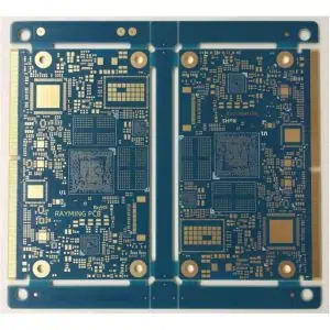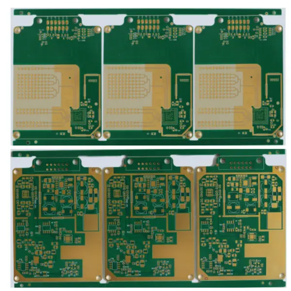
Precision-Engineered Blind Via Technology for Advanced Multi-Layer PCB Applications
Our Blind Via PCB solutions deliver exceptional layer-to-layer connectivity for high-density, multi-layer printed circuit board designs. These specialized vias connect outer layers to inner layers without penetrating the entire board thickness, enabling more compact designs and improved signal integrity.
Key Features
Space-Efficient Design: Blind vias terminate at specific inner layers rather than drilling through the entire PCB stack, maximizing available routing space and allowing for higher component density on both sides of the board.
Enhanced Signal Performance: Shorter via lengths reduce parasitic inductance and capacitance, resulting in improved high-frequency signal transmission and reduced electromagnetic interference (EMI).
Flexible Layer Configuration: Available in various configurations including L1-L2, L1-L3, or custom layer combinations to meet specific design requirements for 4-layer to 20+ layer PCBs.
Superior Manufacturing Quality: Manufactured using advanced laser drilling and plating processes with tight tolerances of ±0.025mm for via diameter and precise depth control.
Technical Specifications
- Via Diameter Range: 0.1mm to 0.35mm (4-14 mils)
- Aspect Ratio: Up to 8:1 for reliable plating
- Minimum Annular Ring: 0.05mm (2 mils)
- Layer Count Compatibility: 4-32 layers
- Material Compatibility: FR4, Rogers, Polyimide, and other advanced substrates
Applications
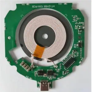
Ideal for high-performance electronics including telecommunications equipment, aerospace systems, medical devices, automotive electronics, and consumer devices requiring miniaturization without compromising functionality.
Quality Assurance: IPC Class 2 and Class 3 compliant with comprehensive AOI inspection, cross-sectional analysis, and electrical testing to ensure reliable interconnections.
Available with lead times of 5-15 days depending on complexity and quantity. Contact our engineering team for custom specifications and design consultation.