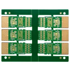
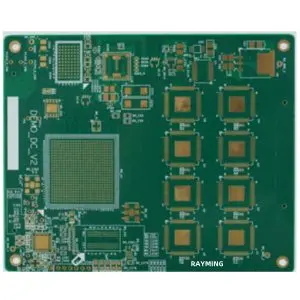
Our 12-layer PCB fabrication service delivers high-performance multilayer printed circuit boards designed for complex electronic applications requiring superior signal integrity, power distribution, and thermal management. These advanced PCBs feature precision-engineered layer stack-ups that maximize functionality while maintaining reliability in demanding environments.
Key Features:
- 12 conductive layers with optimized copper distribution for enhanced current carrying capacity
- Advanced dielectric materials including high-frequency laminates and low-loss substrates
- Controlled impedance matching for critical signal paths and differential pairs
- Dedicated power and ground planes for clean power distribution and EMI shielding
- HDI (High Density Interconnect) capabilities with microvias and blind/buried vias
- Flexible layer configuration customizable to your specific design requirements
Applications: Perfect for high-speed digital systems, RF/microwave circuits, telecommunications equipment, aerospace electronics, medical devices, and advanced computing platforms where signal integrity and power efficiency are critical.
Technical Specifications:
- Layer count: 12 layers
- Board thickness: 1.6mm – 3.2mm (customizable)
- Minimum trace width: 0.1mm (4 mil)
- Via sizes: 0.15mm – 0.8mm
- Copper weight: 1oz – 4oz per layer
- Dielectric materials: FR4, Rogers, Isola, Nelco, and other high-performance substrates
- Surface finishes: HASL, ENIG, OSP, Immersion Silver, Hard Gold
Quality Assurance: Each 12-layer PCB undergoes rigorous testing including electrical continuity, impedance verification, thermal cycling, and automated optical inspection to ensure consistent performance and reliability.
Ideal for engineers and manufacturers requiring sophisticated PCB solutions that deliver exceptional performance in space-constrained, high-frequency applications.