10 pF Capacitor: Crystal Load, RF Filtering & Circuit Uses

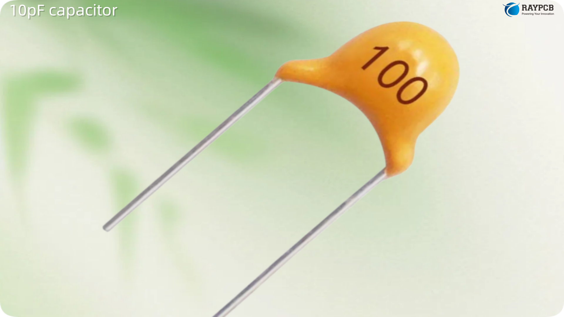
Scroll through any microcontroller reference schematic and you’ll find a pair of identical capacitors flanking a quartz crystal โ€” both labeled 10 pF. Look at the RF section of a Bluetooth or Wi-Fi module and you’ll spot 10 pF appearing again, this time sitting between a supply pin and ground. The 10 pF capacitor is not glamorous, but it is everywhere, and getting it wrong quietly breaks things: oscillators that drift in the cold, RF supplies that radiate spurious emissions, impedance matching networks that deliver mediocre insertion loss. This guide covers every place the 10 pF capacitor shows up, why it works there, how to calculate it correctly, and how to avoid the PCB-level mistakes that undermine it.

What Is a 10 pF Capacitor?

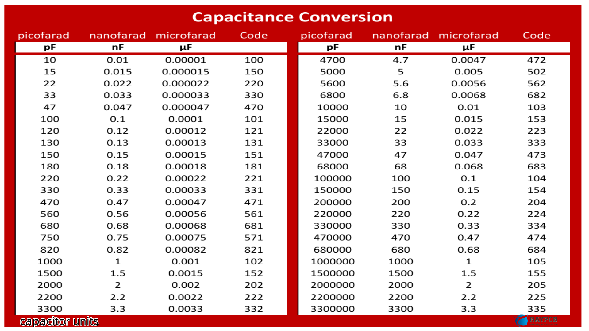
A 10 pF capacitor stores 10 picofarads of charge โ€” 10 ร— 10โปยนยฒ farads. In unit terms that is 0.01 nF or 0.00001 ยตF. Those equivalences matter because component values are listed differently depending on the distributor or schematic tool, and mistaking 10 pF for 10 nF (a factor of 1,000) is a real-world mistake that shows up in production failures more often than engineers like to admit.

At low frequencies the capacitive reactance of a 10 pF capacitor is enormous โ€” tens of thousands of ohms โ€” making it essentially invisible to the circuit. As frequency rises into the tens and hundreds of MHz, that reactance drops into a usable range, which is precisely why 10 pF is one of the most common picofarad values in RF and timing circuits.

Capacitive reactance of 10 pF at common frequencies:

FrequencyApplicationXc of 10 pF
1 MHzLow-frequency RF~15,900 ฮฉ
10 MHzCrystal oscillator (high-speed MCU)~1,592 ฮฉ
100 MHzFM band, basic RF~159 ฮฉ
433 MHzIoT, LoRa~37 ฮฉ
900 MHzGSM, NB-IoT~18 ฮฉ
2.4 GHzWi-Fi, Bluetooth, Zigbee~6.6 ฮฉ
5 GHzWi-Fi 5/6~3.2 ฮฉ

At 900 MHz the reactance is around 18 ฮฉ โ€” squarely within matching network territory. At 10 MHz it sits at over 1.5 kฮฉ, which is why it works as a carefully sized load capacitor for crystal timing circuits without loading the oscillator output heavily.

The 10 pF Capacitor in Crystal Oscillator Circuits

How a Pierce Oscillator Uses Load Capacitors

Almost every microcontroller’s onboard oscillator uses a Pierce topology. In a Pierce oscillator, the crystal connects between two IC pins (typically XTAL_IN and XTAL_OUT), with a load capacitor from each pin to ground โ€” labeled CL1 and CL2. These two capacitors, along with the crystal itself and the stray PCB capacitance, determine the total load capacitance (CL) seen by the crystal.

The crystal manufacturer specifies the CL value at which the crystal oscillates at its nominal frequency. Get CL wrong and the crystal runs off-frequency โ€” sometimes by tens of ppm, which in a Bluetooth or Zigbee device translates directly to channel center frequency error and failed regulatory compliance.

The Load Capacitance Formula

The total effective load capacitance is calculated as:

CL = (CL1 ร— CL2) / (CL1 + CL2) + Cstray

Where CL1 = CL2 (you should use matched values) and Cstray is the combined capacitance of the IC pins and PCB traces. Stray capacitance in a Pierce oscillator circuit usually ranges from 3 pF to 7 pF. On a two-layer board with short traces it may be as low as 2 pF; on a dense four-layer board closer to 5 pF.

Solving for CL1 and CL2 When CL = 10 pF

Many modern RF-enabled MCUs (STM32 families, TI CC26xx, nRF52 series) use crystals with a specified load capacitance of 6โ€“10 pF. The “10 pF CL” crystal is a common, well-stocked value. Here is how to solve for the external capacitors:

CL1 = CL2 = 2 ร— (CL โˆ’ Cstray)

Using CL = 10 pF and assuming Cstray = 4 pF (typical for a modern 4-layer board):

CL1 = CL2 = 2 ร— (10 โˆ’ 4) = 12 pF

If your actual Cstray is higher than estimated, the external capacitors should be reduced. If the measured oscillator frequency is consistently too low, effective CL is too high โ€” reduce the external capacitors. If the frequency is consistently high, increase them. The 10 pF value commonly appears as the final calculated value for CL1/CL2 when the target crystal CL is higher (e.g., 12โ€“15 pF) and stray capacitance consumes some of the budget.

Common Crystal Load Capacitor Scenarios

Crystal CLAssumed CstrayRequired CL1 = CL2
6 pF3 pF6 pF
8 pF3 pF10 pF โ† common 10 pF case
10 pF4 pF12 pF
12 pF4 pF16 pF
18 pF5 pF26 pF

The “10 pF external capacitor for crystal loading” scenario appears whenever the crystal’s CL is around 8 pF and stray capacitance is moderate โ€” a common combination in compact IoT and Bluetooth designs.

10 pF as an RF Decoupling and Bypass Capacitor

Why 10 pF and 33 pF Are Classic RF Supply Bypass Values

In RF engineering, power supply pins of LNAs, PAs, mixers, and VCOs must be bypassed to ground to prevent RF energy from coupling back into the supply rails โ€” which causes instability, spurious outputs, and unwanted oscillation. The bypass capacitor must look like a very low impedance at the RF operating frequency.

The 10 pF and 33 pF capacitors achieved classic status in this role for a specific reason: in C0G/NP0 dielectric and 0603 packaging, their self-resonant frequency (SRF) lands close to important RF bands. At SRF, the capacitor’s impedance is at its lowest โ€” essentially only its ESR remains. This “free filtering” effect at the SRF is deliberately exploited in RF circuit design.

For the 10 pF value in a 0402 package with approximately 0.5 nH of ESL:

SRF โ‰ˆ 1 / (2ฯ€ ร— โˆš(0.5ร—10โปโน ร— 10ร—10โปยนยฒ)) โ‰ˆ 2.25 GHz

That puts the SRF right in the 2.4 GHz ISM band โ€” one reason 10 pF appears so often as a bypass element in Wi-Fi and Bluetooth power supply networks.

RF Bypass Capacitor Strategy

In practice, a single capacitor value never covers the full frequency range of noise on a supply pin. A multi-cap strategy using a 10 pF (for high-frequency bypassing) alongside a 100 nF (mid-frequency) and a 10 ยตF bulk cap provides broadband impedance suppression across decades of frequency. The 10 pF handles the GHz range; the other values handle lower frequencies.

10 pF in RF Matching and Filter Networks

Reactance in Matching Networks at Sub-1 GHz

At 433 MHz, 10 pF delivers about 37 ฮฉ of reactance. That value slots neatly into L-network calculations for antenna matching networks in LoRa, ISM-band, and RFID circuits. Many reference designs for 433/868/915 MHz front-ends include a 10 pF shunt or series element in the output matching network between the PA and the antenna port.

LC Filter Elements

In a Chebyshev or Butterworth bandpass filter for a 900 MHz front-end, the component values that fall out of the design equations commonly land in the 10โ€“47 pF range for the capacitor elements. The 10 pF is a natural fit for narrow-band filters where tighter selectivity is needed. It also appears in SAW filter input/output matching networks and LNA interstage networks.

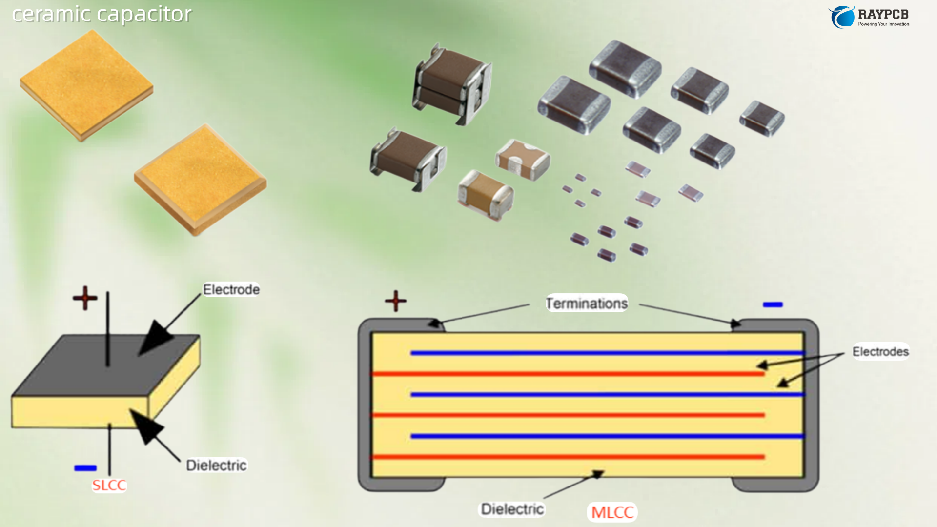
Dielectric and Package Selection for 10 pF

Always Use C0G/NP0 in Timing and RF Circuits

The choice of dielectric is not optional for a 10 pF in crystal load or RF matching service. Class II dielectrics like X7R have significant capacitance variation with temperature and DC bias voltage. For a 10 pF crystal load capacitor, a 5% capacitance shift with temperature moves the crystal frequency by several ppm โ€” unacceptable in timing-critical or RF-compliant designs. C0G (NP0) provides ยฑ30 ppm/ยฐC temperature stability, Q factor exceeding 1,000, and effectively zero voltage dependence.

DielectricTemp StabilityVoltage DependenceQ Factor10 pF Crystal Load?10 pF RF Bypass?
C0G / NP0ยฑ30 ppm/ยฐCNone>1000โœ… Requiredโœ… Preferred
X7Rยฑ15% over rangeModerate100โ€“500โŒ Not suitableโš ๏ธ Only if SRF-targeted
X5Rยฑ15% over rangeHigh<300โŒ Not suitableโŒ Avoid

Package Size and SRF Implications

PackageTypical ESLApproximate SRF for 10 pF
0201 (0603M)~0.3 nH~9 GHz
0402 (1005M)~0.5 nH~7.1 GHz
0603 (1608M)~0.8 nH~5.6 GHz
0805 (2012M)~1.0 nH~5.0 GHz

For 2.4 GHz applications, any of these packages provides adequate SRF margin. For 5 GHz Wi-Fi designs, 0402 or 0201 is recommended to keep SRF comfortably above the operating frequency.

PCB Layout Tips for 10 pF Applications

Getting the component right and then ruining it with bad layout is the most common failure mode when working with picofarad-range capacitors.

Crystal load capacitors: Place CL1 and CL2 as close to the crystal pins as possible โ€” ideally within 1 mm. Trace lengths to the crystal should be short and equal. Keep the crystal circuit away from high-speed digital signals and switching regulators. A ground plane under the crystal area is generally not recommended by many MCU manufacturers because it adds stray capacitance and can destabilize the oscillator.

RF bypass capacitors: The ground via for a shunt bypass capacitor must be as close as possible to the component pad โ€” not routed through a long trace to a distant via. A typical via adds 0.4โ€“0.8 nH of inductance, which at 2.4 GHz is measurable. For demanding RF designs, use a via-in-pad approach or place the via immediately adjacent to the ground pad.

Pad sizing: Oversized pads add extra capacitance to ground. For a 10 pF component, even 0.5โ€“1 pF of additional pad capacitance shifts the value by 5โ€“10%. Use the component manufacturer’s recommended land pattern and do not arbitrarily enlarge pads for “better soldering.”

Trace stubs: Any trace between a 10 pF capacitor and the next RF node acts as a stub. At 2.4 GHz even 1 mm of trace introduces a few tenths of a nanohenry of inductance. Keep connections as direct as possible and simulate with layout parasitics included.

10 pF Capacitor Specification Checklist

ParameterRecommended Specification
Capacitance10 pF
Toleranceยฑ0.5 pF for crystal load; ยฑ1 pF acceptable for RF bypass
DielectricC0G / NP0
Voltage ratingโ‰ฅ10 V (typically 25 V or 50 V for MLCC)
Package0402 for most designs; 0201 for 5 GHz+
Operating temperatureโˆ’55ยฐC to +125ยฐC
SRFVerify it exceeds operating frequency by โ‰ฅ2ร—
ESR<0.3 ฮฉ at operating frequency
QualificationAEC-Q200 for automotive; standard EIA-198 otherwise

Useful Resources for 10 pF Capacitor Selection and Crystal Design

ResourceTypeLink
ECS Inc. Crystal Load Capacitance CalculatorOnline toolecsxtal.com
ECS Inc. โ€“ Impact of Load Capacitance on Crystal DesignsWhitepaperecsxtal.com
Texas Instruments AN โ€“ Crystal & Oscillator Selection (CC13xx/CC26xx)App noteti.com
AllAboutCircuits โ€“ Load Capacitance on Quartz CrystalsTechnical articleallaboutcircuits.com
Johanson Technology โ€“ SRF/PRF for RF CapacitorsApplication notejohansontechnology.com
KYOCERA AVX โ€“ C0G/NP0 Dielectric OverviewProduct referencekyocera-avx.com
Murata SimSurfing โ€“ S-parameter search toolComponent databaseds.murata.co.jp/simsurfing
RayPCB โ€“ Capacitors in PCB DesignPCB design guideraypcb.com/pcb-capacitor

Frequently Asked Questions

1. Can I use an X7R 10 pF capacitor for crystal load capacitors?

In general, no. X7R capacitance varies with temperature โ€” typically ยฑ15% over the operating range. A 10% shift in a 10 pF load capacitor will pull the crystal frequency by several ppm, which exceeds the tolerance of any serious timing application. For a microcontroller clock where the Bluetooth stack tolerates ยฑ20โ€“40 ppm total, using X7R for the load capacitors is a real design risk. Always specify C0G/NP0 for crystal load applications.

2. My crystal datasheet says CL = 10 pF. Does that mean I use 10 pF capacitors for CL1 and CL2?

No โ€” this is one of the most common misconceptions. The crystal CL is the total capacitive load the crystal must see from the circuit. CL1 and CL2 are in series (from the crystal’s perspective through ground), so two equal external capacitors of value C produce a series combination of C/2. You also need to subtract the stray capacitance of the PCB and IC pins. Using the formula CL1 = CL2 = 2 ร— (CL โˆ’ Cstray), with CL = 10 pF and Cstray โ‰ˆ 3โ€“4 pF, you end up with approximately 12โ€“14 pF for each external capacitor โ€” not 10 pF.

3. Why do 10 pF and 33 pF appear so often in RF supply bypass circuits?

These values became widely adopted because, in older 0603 packages, their self-resonant frequencies (SRFs) landed near the 900 MHz and 2.4 GHz ISM bands respectively โ€” providing a very low impedance “for free” at important wireless frequencies. Although modern 0402 and 0201 packages have shifted SRFs upward, the habit of reaching for 10 pF or 33 pF for RF supply bypassing has stuck because they still produce useful low impedance in the GHz range with appropriate package selection.

4. How do I know if my 10 pF capacitor is causing a crystal oscillator failure?

The most reliable diagnostic is to measure the actual oscillation frequency using the MCU’s clock output pin (MCO or similar) with a frequency counter while varying temperature. If the frequency drifts outside the crystal’s specified tolerance window as temperature changes, first suspect the load capacitor dielectric (check for X7R) and pad layout stray capacitance. If the oscillator fails to start reliably at cold temperatures, check oscillator gain margin โ€” the crystal’s equivalent series resistance (ESR) rises at low temperature, and if combined with excessive load capacitance, the gain margin falls below unity.

5. Does PCB layer count significantly affect the 10 pF crystal load capacitor value I should use?

Yes, noticeably. Stray capacitance Cstray varies with PCB design: a two-layer board with short traces may contribute only 1โ€“2 pF of stray capacitance, while a dense four-layer board with longer crystal trace routing and more copper nearby may contribute 4โ€“6 pF. If you calculated CL1/CL2 assuming Cstray = 3 pF but your board actually has 6 pF of stray, you’ll end up overloading the crystal and running slightly below the nominal frequency. Always verify oscillator frequency on the first prototype and adjust the capacitor values accordingly before committing to production.

Conclusion

The 10 pF capacitor is deceptively ordinary in appearance but technically demanding in application. Whether it’s sitting in a Pierce oscillator circuit setting the load capacitance of a 10 MHz crystal reference, bypassing the supply of a 2.4 GHz PA, or forming part of a narrowband antenna matching network, the rules are the same: use C0G/NP0 dielectric without exception, choose the right package for your operating frequency and SRF requirements, get the tolerances tight, and treat the PCB layout around it with the same discipline you’d apply to any other RF element. A few extra minutes of correct calculation and careful placement avoids the kind of production-line frequency drift or RF spurious issue that takes days to debug on a scope.

4.7 pF Capacitor: Applications in RF, Oscillators & Load Matching

Everything you need to know about the 4.7pF capacitor: RF matching, crystal oscillator load capacitance, C0G vs X7R dielectric, 0402 vs 0201 package selection, real part numbers, and PCB layout tips for GHz-range designs.

If you’ve spent time designing RF front-ends, crystal oscillator circuits, or high-frequency filters, you’ve almost certainly landed on a 4.7 pF capacitor at some point. It’s one of the most useful values in the sub-10 pF range โ€” large enough to be relatively forgiving in terms of parasitic effects compared to 1 pF, yet small enough to be useful in matching networks and load capacitance tuning well above 1 GHz.

The challenge with a 4.7pF capacitor is that most engineers treat it like any other bypass cap โ€” slap down an X7R MLCC and call it done. That approach works fine at low frequencies, but at RF frequencies it can silently ruin your circuit performance without any obvious component failure. This guide covers the real applications, the specs that actually matter, how to pick the right package, and where to source parts that will perform as expected.

What Is a 4.7 pF Capacitor?

A 4.7 pF capacitor stores 4.7 picofarads of charge โ€” that’s 4.7ร—10โปยนยฒ farads. In the standard E12 capacitor series, 4.7 pF falls between 3.9 pF and 5.6 pF. In the E24 series, it sits between 4.3 pF and 5.1 pF. The value is widely stocked in ceramic chip form across multiple package sizes.

At this capacitance level, the reactance (Xc = 1 / 2ฯ€fC) at common RF frequencies is:

FrequencyReactance of 4.7 pF
100 MHz338 ฮฉ
433 MHz78 ฮฉ
915 MHz37 ฮฉ
2.4 GHz14 ฮฉ
5.8 GHz5.8 ฮฉ

This reactance range maps directly onto why 4.7 pF shows up in so many RF impedance matching and filter applications between 400 MHz and 3 GHz. At sub-GHz frequencies, it presents a high enough impedance to be useful as a series element; at 2.4 GHz and above, it’s useful as a shunt element in matching networks.

Like all small-value ceramics, a 4.7pF capacitor performs very differently depending on dielectric type, package size, and PCB layout. Understanding those differences is what separates a design that hits spec from one that needs three board respins.

Key Applications of the 4.7 pF Capacitor

RF Impedance Matching Networks

This is the most demanding application for a 4.7pF capacitor. In L-network, pi-network, and T-network matching topologies used to interface antennas, LNAs, PAs, and mixers to a 50 ฮฉ system, the component values are calculated from the source and load impedances and the target center frequency. For frequencies between 400 MHz and 2.4 GHz, calculated capacitance values regularly land in the 2โ€“10 pF range, making 4.7 pF one of the most frequently specified values.

The reactance tolerance matters here. A ยฑ5% tolerance on 4.7 pF means the actual value could be anywhere from 4.47 pF to 4.94 pF. At 2.4 GHz, that’s a reactance variation of roughly ยฑ0.7 ฮฉ โ€” potentially significant in a narrow-band matching network. For production-intent designs, specify ยฑ0.25 pF or ยฑ0.1 pF absolute tolerance.

Crystal Oscillator Load Capacitance

The most common application many digital engineers encounter for a 4.7pF capacitor is in crystal oscillator circuits. A Pierce oscillator (used in virtually all microcontroller crystal circuits) requires two capacitors โ€” one from each oscillator pin to ground โ€” to present the correct load capacitance to the crystal.

For a crystal with a specified load capacitance C_L, the two external caps are ideally:

C_ext = 2 ร— (C_L โˆ’ C_stray)

where C_stray accounts for PCB trace capacitance and the MCU pin capacitance (typically 2โ€“5 pF total). For crystals with C_L = 12 pF, C_ext often works out to 12โ€“18 pF per leg after accounting for series parasitic capacitance. But for lower-load-capacitance crystals (C_L = 6โ€“9 pF, increasingly common in low-power and high-frequency crystals), the external capacitors can drop to 4.7 pF or below.

Using the wrong load capacitance shifts the crystal’s operating frequency. For a 32 MHz crystal with a frequency pulling sensitivity of 20 ppm/pF, a 1 pF error in load capacitance causes a 20 ppm frequency error โ€” enough to fail USB timing requirements or cause Bluetooth channel spacing issues.

Antenna Tuning and Matching

Chip antennas for 2.4 GHz (WiFi, BT, Zigbee) and sub-GHz ISM bands almost always require an external matching network to tune the antenna impedance to 50 ฮฉ at the RF IC port. Most chip antenna manufacturers provide a reference matching network in their datasheet, and 4.7 pF is a very common shunt or series element in those networks.

When a PCB is slightly different from the reference design โ€” different board size, different ground plane geometry, different substrate โ€” the antenna impedance shifts and the matching network needs retuning. Having a 4.7 pF cap (or neighboring values like 3.9 pF and 5.6 pF) in your retuning toolkit is standard practice.

RF Filter Design

In discrete LC bandpass, low-pass, and high-pass filters for RF systems, 4.7 pF appears frequently as a shunt or series capacitor in designs for 433 MHz, 868 MHz, 915 MHz, and 2.4 GHz. It’s particularly common in harmonic filters placed after power amplifiers to meet regulatory spurious emission limits.

The Q factor of the capacitor directly affects the filter’s insertion loss and shape factor. A low-Q cap (high ESR) in a filter will add passband insertion loss and round off the filter skirts. For filter applications, specify caps with Q > 200 at the operating frequency.

VCO Tank Circuit Trimming

In voltage-controlled oscillators, the tank circuit capacitance sets the center frequency. A fixed capacitor placed in parallel with the varactor diode (or as part of the tank capacitance) sets the baseline around which the varactor tunes. At 433โ€“915 MHz, these fixed tank caps are often in the 4โ€“10 pF range, making 4.7 pF a natural fit.

High-Speed PCB AC Coupling

In some high-speed differential or RF signal chains, AC coupling capacitors are chosen small enough to maintain a flat response through the operating band while blocking DC. At 2.4 GHz and above, a 4.7 pF coupling cap presents about 14 ฮฉ โ€” low enough to pass the signal with minimal insertion loss while blocking DC offset.

Choosing the Right Package for a 4.7 pF Capacitor

Package selection affects parasitic inductance, parasitic capacitance, self-resonant frequency (SRF), and Q factor. For RF applications, smaller is generally better โ€” up to the point where assembly yield becomes a concern.

PackageSize (mm)Typical SRF (4.7 pF)Pad Parasitic CBest For
0603 (1608M)1.6 ร— 0.8~3โ€“5 GHz~0.3 pFGeneral purpose, easy to solder
0402 (1005M)1.0 ร— 0.5~5โ€“8 GHz~0.15 pFRF up to 3 GHz, standard RF production
0201 (0603M)0.6 ร— 0.3~8โ€“12 GHz~0.07 pF5 GHz and above, lower parasitics
01005 (0402M)0.4 ร— 0.2>12 GHz<0.05 pFmmWave, specialized assembly only

For most RF work at 433 MHz to 3 GHz, 0402 is the right choice. It balances low parasitics with practical assembly requirements. Move to 0201 if you’re designing above 3 GHz or if you’re doing a comparative placement trial to measure layout parasitics.

Dielectric Selection: Why C0G Is Non-Negotiable for RF

This is one of the most common specification errors on RF PCBs. There are three main MLCC dielectric classes you’ll encounter:

DielectricCapacitance Stability vs TempCapacitance vs VoltageUse in RF Circuits
C0G (NP0)ยฑ30 ppm/ยฐC (excellent)No changeYes โ€” always preferred
X7Rยฑ15% over โˆ’55 to +125ยฐCDegrades with DC biasAvoid for RF/oscillator use
Y5V+22% / โˆ’82% over temp rangeSeverely degrades with biasNever use in RF circuits

For a 4.7pF capacitor in a matching network or oscillator circuit, C0G (NP0) is the only acceptable dielectric. X7R capacitance drifts by up to 15% over temperature โ€” for a 4.7 pF cap, that’s a swing of nearly 0.7 pF, which will detune your matching network and pull your oscillator frequency. C0G caps cost a bit more, but the difference is negligible in any RF design where performance matters.

Recommended 4.7 pF Capacitor Part Numbers

ManufacturerPart NumberPackageDielectricToleranceVoltage
MurataGRM1555C1H4R7BA01D0402C0Gยฑ0.1 pF50 V
TDKC1005C0G1H4R7C050BA0402C0Gยฑ0.25 pF50 V
KemetC0402C479C5GACTU0402C0Gยฑ0.25 pF50 V
VishayVJ0402A4R7CXACW1BC0402C0Gยฑ0.1 pF50 V
Wรผrth Elektronik8850120050170402C0Gยฑ0.1 pF50 V
AVX/Kyocera04025A4R7BAT2A0402C0Gยฑ0.1 pF50 V
ATC100B4R7BW500XTATC 100BC0Gยฑ0.1 pF500 V

The ATC 100B series is worth calling out specifically for high-power RF applications (PA harmonic filters, antenna switches) where a standard MLCC would fail under RF current stress. The capacitor construction in these high-Q RF chip caps is fundamentally different from standard MLCCs.

PCB Layout Guidelines for 4.7 pF Capacitors in RF Circuits

Use the manufacturer’s recommended land pattern. Pad dimensions directly affect parasitic capacitance. An oversized 0402 pad pattern can add 0.1โ€“0.3 pF of stray capacitance โ€” up to 6% of your intended 4.7 pF value.

Consider a ground plane void beneath series capacitors. For caps placed in a series RF signal path, a small copper void (clearance cutout) in the ground plane beneath the cap reduces parasitic shunt capacitance to ground. This is especially important at 2.4 GHz and above.

Keep matching network components close together and close to the antenna or RF port. Trace length between matching elements adds inductance and changes the network’s effective topology. Route matching caps with the shortest possible traces directly to the pad.

Run EM simulation before fabrication. At 2.4 GHz and above, even the shape of your pad and the trace routing around a 4.7 pF cap can shift the effective capacitance enough to detune a matching network. Sonnet Lite (free), Ansys HFSS, or Cadence AWR can extract parasitic effects from your layout before committing to fab.

Separate matching network ground vias from digital return currents. A single via shared between the matching network ground and a switching regulator return path can inject noise into the RF circuit. Keep RF ground returns isolated and stitched directly to the RF ground plane.

Where to Buy 4.7 pF Capacitors

DistributorWebsiteNotes
Digi-Keydigikey.comBest parametric search, huge stock depth
Mousermouser.comStrong authorized stock for Murata, TDK, KEMET
LCSClcsc.comCost-effective for prototyping quantities
Arrowarrow.comGood for production volumes with traceability
Farnell/Element14farnell.comEU/UK preferred distributor for authorized stock

For production runs, always buy through authorized distributors with full traceability. Counterfeit small-value ceramics are more common than most engineers expect, and the failure mode is insidious โ€” the fake caps often measure close to spec on an LCR meter but perform poorly at RF frequencies due to inferior dielectric or electrode materials.

Useful Resources and Design Tools

  • Murata SimSurfingย โ€“ Free online tool to view impedance, ESR, and S-parameters vs. frequency for Murata capacitors: ds.murata.com/simsurfing
  • Kemet KSIMย โ€“ Capacitor simulation with impedance and insertion loss curves: ksim.kemet.com
  • TDK Product Finder with S-parameter Downloadsย โ€“ Full parametric search with downloadable SPICE/S-param models: product.tdk.com
  • ATC RF Capacitor Datasheet Libraryย โ€“ High-Q RF chip caps with full S-parameter data for microwave design: atceramics.com
  • Sonnet Lite (Free EM Simulator)ย โ€“ Layout-level EM simulation for RF circuits: sonnetsoftware.com
  • Texas Instruments Crystal Oscillator Design Reference (AN-2447)ย โ€“ Detailed guide on load capacitance calculation for Pierce oscillators
  • Wรผrth Elektronik ANP008ย โ€“ Application note on three-terminal caps, RF filtering, and parasitic effects: we-online.com
  • Mini-Circuits RF Calculatorsย โ€“ L-network and pi-network matching calculators: minicircuits.com

Frequently Asked Questions About 4.7 pF Capacitors

Can I substitute a 4.7 pF capacitor with 4.3 pF or 5.1 pF in a matching network?

Often yes โ€” with simulation and measurement. In an RF matching network, the center frequency and impedance transformation depend on the exact component values. Swapping 4.7 pF for 4.3 pF or 5.1 pF will shift the network’s response, but depending on the bandwidth of the network, the change may be tolerable. Always re-simulate with the new value and verify on hardware with a VNA before committing to the change in production.

Why does my 4.7 pF capacitor measure differently on my LCR meter than its spec?

Low-value capacitors are sensitive to measurement frequency, lead placement, and stray capacitance in the test fixture. Most LCR meters measure at 1 kHz or 1 MHz by default, which may not match the frequency at which the cap was characterized in its datasheet. Also, probe leads and the PCB itself contribute parasitic capacitance that can add 0.5โ€“1 pF or more to the reading. Open-compensation and short-compensation in the LCR meter’s fixture calibration helps, but some residual error is unavoidable at 4.7 pF.

What happens if I use X7R instead of C0G for a 4.7 pF cap in an oscillator circuit?

You’ll likely see oscillator frequency drift with temperature that exceeds the crystal’s own temperature coefficient. X7R capacitance can change by ยฑ15% over the operating temperature range. For a 4.7 pF cap, that’s up to ยฑ0.7 pF variation. In a crystal load capacitance context, a 1 pF change in total load capacitance can pull the oscillator frequency by 10โ€“30 ppm depending on the crystal’s motional parameters โ€” enough to cause real problems in wireless or USB clock applications. Use C0G.

How do I account for PCB parasitic capacitance when placing a 4.7 pF cap?

Start by estimating the parasitic contribution from your layout: typical 0402 pad pair adds ~0.1โ€“0.2 pF, a short trace to a via adds ~0.1โ€“0.3 pF/mm, and a via itself adds ~0.3โ€“0.8 pF depending on board stackup and aspect ratio. Sum these up and subtract from your target capacitance to get the component value you actually need to specify. If the parasitics are comparable to your intended 4.7 pF, use EM simulation to get a more accurate parasitic estimate before ordering parts.

Is a 4.7 pF capacitor suitable for power supply decoupling?

Technically yes, but it’s generally too small to be useful as a standalone decoupling cap in any power supply context. At 100 MHz, a 4.7 pF cap presents about 338 ฮฉ โ€” far too high for effective high-frequency decoupling. You’d use 100 nF or 10 nF for bulk and high-frequency decoupling, and possibly a 1โ€“10 pF cap only as a supplementary high-frequency bypass in very specific RF power supply situations. In standard digital or analog power supply design, a 4.7 pF cap has no practical decoupling role.

Working with a 4.7pF capacitor well comes down to three things: specifying C0G dielectric every single time, choosing the right package for your frequency range, and respecting the role that PCB layout plays at values this small. Get those right and a 4.7 pF cap in a matching network or oscillator circuit will hit your targets. Get them wrong and you’ll spend debugging time on a problem that was never really a circuit topology issue in the first place.

4.7nF Capacitor (Code 472): RC Filter Design, Dielectric Selection & PCB Layout Guide

Decode capacitor code 472, select C0G vs X7R dielectric, and calculate RC filter cutoffs for the 4.7nF capacitor โ€” practical guide from a PCB engineer’s perspective.

The 4.7nF capacitor is one of those parts that sits in the E12/E24 standard value series and gets pulled into designs constantly โ€” from ADC anti-aliasing filters and RF snubbers to debounce networks and CFL ballasts. Yet when a junior engineer looks at the body of a ceramic disc and sees 472, confusion often follows. What does it mean, and what can this capacitor actually do for your circuit?

This guide answers both questions from the ground up. By the end, you’ll know how to decode the marking, select the right dielectric, calculate RC filter cutoff frequencies, and lay the part out correctly on your PCB.

Decoding Capacitor Code 472: What Does It Mean?

The EIA three-digit marking system is straightforward once you know the rule: the first two digits are significant figures, and the third digit is the power-of-ten multiplier in picofarads.

DigitValueMeaning
1st4First significant figure
2nd7Second significant figure
3rd (multiplier)2ร— 10ยฒ = ร— 100
Result4700 pF = 4.7 nF = 0.0047 ยตFAll equivalent

So 47 ร— 100 = 4700 pF = 4.7 nF. Simple as that. You’ll see this part listed under all three unit conventions depending on the distributor. They are identical โ€” 4.7 nF, 4700 pF, and 0.0047 ยตF are the same capacitance.

One trap to watch for: 473 is not the same as 472. The 473 decodes to 47 ร— 1000 = 47,000 pF = 47 nF โ€” a full ten times larger. Getting these mixed up on a BOM is a real design risk, especially when similar-looking parts sit next to each other in a reel drawer.

A tolerance letter suffix usually follows the three digits. J = ยฑ5%, K = ยฑ10%, M = ยฑ20%. The voltage rating may also appear as a prefix letter-number pair (e.g., 2A = 100 VDC per EIA standard), though on smaller disc ceramics this is often absent โ€” check the datasheet or reel label.

4.7nF Capacitor Full Specifications

ParameterTypical Values
Capacitance4.7 nF (4700 pF / 0.0047 ยตF)
EIA Marking Code472
Common DielectricsC0G/NP0, X7R, Y5V
Voltage Ratings16V, 25V, 50V, 100V, 250V, 400V, 1000V+
Toleranceยฑ5% (J), ยฑ10% (K), ยฑ20% (M)
SMD Packages0402, 0603, 0805, 1206
Through-Hole PackagesRadial disc, film (5mm, 10mm pitch)
ESRLow โ€” suitable for RF and high-frequency circuits
Polarised?No โ€” non-polarised in all types

Choosing the Right Dielectric for Your 4.7nF Capacitor

This is where component selection either goes right or quietly causes you a re-spin six months down the road. The dielectric you choose defines how the 4.7nF capacitor will actually behave in your circuit โ€” not just at room temperature on the bench, but across its entire operating range.

C0G / NP0 โ€” The Precision Choice

C0G (also called NP0) is a Class 1 dielectric with a temperature coefficient typically within ยฑ30 ppm/ยฐC. In practice this means negligible capacitance change over โˆ’55ยฐC to +125ยฐC, no measurable aging, and no voltage-dependent capacitance shift. The dissipation factor is also extremely low (maximum 0.15%), which translates to minimal signal loss at high frequencies.

For any 4.7nF capacitor that sits in a timing circuit, oscillator feedback network, precision analog filter, or RF tuning stage, C0G is the correct choice. Yes, it’s slightly larger for a given capacitance-voltage combination compared to X7R, but in the nF range this is rarely a problem. You can fit a C0G 4.7nF in an 0603 package at 50V without issue.

X7R โ€” Workhorses for General-Purpose Filtering

X7R allows ยฑ15% capacitance variation over โˆ’55ยฐC to +125ยฐC, and it ages logarithmically โ€” roughly 1โ€“2% capacitance loss per decade-hour. For non-critical decoupling, power supply bypass, or filtering stages where the exact โˆ’3dB point doesn’t need to be tightly controlled, X7R is cost-effective and compact.

However, be conscious of DC bias derating. An X7R 4.7nF capacitor rated at 50V can lose a significant portion of its nominal capacitance when operated at a high fraction of its rated voltage. Always check the manufacturer’s DC bias curve in the datasheet, not just the nominal value.

Y5V / Z5U โ€” Avoid for Signal Work

Capacitance can vary by as much as โˆ’82% across the operating temperature range. Not appropriate for filters, timing, or any circuit where the RC time constant must be predictable. Reserve these for bulk energy storage where capacitance tolerance is irrelevant to function.

Dielectric Selection Summary

DielectricTemp StabilityAgingDC Bias EffectBest For
C0G / NP0ยฑ30 ppm/ยฐCNegligibleNoneFilters, timing, RF, oscillators
X7Rยฑ15% over range~1โ€“2%/decadeModerateGeneral decoupling, bypass
Y5V+22% / โˆ’82%HighSignificantBulk storage only

RC Filter Design with a 4.7nF Capacitor

The core formula for an RC filter cutoff frequency is:

fc = 1 / (2ฯ€ ร— R ร— C)

With C = 4.7 nF, this gives the following โˆ’3 dB cutoff frequencies across standard resistor values:

Resistor (R)Cutoff Frequency (fc)Suggested Application
33 ฮฉ~1.02 MHzHF RF snubber, EMI suppression
100 ฮฉ~338 kHzHigh-speed signal line filtering
1 kฮฉ~33.8 kHzADC input conditioning
3.38 kฮฉ~10 kHzAudio band low-pass
10 kฮฉ~3.38 kHzMid-frequency signal filtering
33.8 kฮฉ~1 kHzLow-frequency anti-aliasing
100 kฮฉ~338 HzAudio high-pass, DC blocking

At the cutoff frequency, output voltage is at 70.7% (โˆ’3 dB) of input. Below that for a low-pass filter, the signal passes through with minimal attenuation. Above it, roll-off occurs at โˆ’20 dB per decade for a single-pole stage.

How to Reverse-Calculate the Resistor for a Target Cutoff

Rearranging the formula: R = 1 / (2ฯ€ ร— fc ร— C)

Example: You need a 5 kHz low-pass filter with your 4.7nF capacitor:

R = 1 / (2ฯ€ ร— 5000 ร— 4.7ร—10โปโน) = 6.76 kฮฉ

The nearest E24 standard value is 6.8 kฮฉ, which gives a cutoff of approximately 4.98 kHz โ€” effectively spot on.

RC Time Constant for Timing Circuits

For timing applications, the time constant ฯ„ = R ร— C determines how quickly the capacitor charges to ~63.2% of supply voltage:

Resistor (R)Time Constant (ฯ„)Typical Use Case
1 kฮฉ4.7 ยตsHigh-speed pulse timing
10 kฮฉ47 ยตsMid-range timing, debounce
47 kฮฉ220.9 ยตsOscillator RC networks
100 kฮฉ470 ยตsTimer stages, 555 astable
470 kฮฉ2.209 msSlow timing intervals

A complete charge cycle is conventionally taken at 5ฯ„ (~99.3%). If you’re using the 4.7nF with a 555 timer, pairing it with a 47 kฮฉ resistor puts your oscillation frequency in the tens of kilohertz range โ€” a common sweet spot for tone generators and basic PWM.

Where the 4.7nF Capacitor Gets Used on Real PCBs

The 4.7nF capacitor covers a distinctive frequency territory that makes it a regular fixture in several circuit categories:

ADC anti-aliasing filters are one of the most common placements. High-speed ADCs typically require a low-pass RC filter at the input to prevent frequency aliasing. The 4.7nF paired with a resistor in the 1โ€“10 kฮฉ range covers the audio-to-RF boundary well.

RF and microwave snubbers use the 4.7nF to suppress switching transients on gate drive lines and MOSFET drain nodes. At these frequencies, low ESR is critical โ€” use C0G ceramic in 0402 or 0603.

IยฒC and SPI bus filtering in noisy industrial environments often benefits from a small capacitor to ground on each signal line. The 4.7nF is a common choice here because it provides good HF suppression without visibly slowing down the signal edges at standard bus speeds.

**CFL ballast networks

2.2 pF Capacitor: Tiny Value, Big Role in RF Matching

2.2 pF capacitor delivers ~30 ฮฉ reactance at 2.4 GHz โ€” making it essential for RF matching. Learn dielectric selection, PCB layout tips, and spec guidance.

Pick up a 0402-size 2.2 pF capacitor and you can barely see it. Under a microscope it looks unremarkable โ€” a beige ceramic chip with two silver terminations. But drop it into an RF matching network at 5 GHz and that single component can mean the difference between a clean โˆ’30 dB return loss and a system that reflects half its power back into the amplifier. If you’ve spent any time laying out antenna matching networks, power amplifier output stages, or LNA input circuits, you already know the pF-range capacitor range is where precision engineering actually lives.

This article covers everything you need to get the most out of the 2.2 pF capacitor: what makes it behave the way it does at GHz frequencies, where it belongs in a circuit, which dielectric to choose, how PCB layout can ruin it even after you’ve specified it correctly, and how to buy the right part from the right manufacturer.

What Is a 2.2 pF Capacitor and Why Does That Value Matter?

A 2.2 pF capacitor stores 2.2 picofarads of charge โ€” 0.0000000000022 farads. In a DC or low-frequency context, that’s essentially nothing. But capacitive reactance follows the formula:

Xc = 1 / (2ฯ€ ร— f ร— C)

At RF and microwave frequencies, that tiny capacitance translates into impedance levels that sit squarely in the range of typical RF circuit impedances (typically 50 ฮฉ, sometimes 75 ฮฉ). Here’s why it matters โ€” look at what 2.2 pF produces at common wireless frequencies:

FrequencyApplicationXc of 2.2 pF
100 MHzFM radio, basic RF~723 ฮฉ
433 MHzIoT, LoRa~168 ฮฉ
900 MHzGSM, LPWAN~80 ฮฉ
1.575 GHzGPS L1~46 ฮฉ
2.4 GHzWi-Fi, Bluetooth, Zigbee~30 ฮฉ
5 GHzWi-Fi 5/6, 5G Sub-6~14.5 ฮฉ
24 GHzAutomotive radar, mmWave~3 ฮฉ

Notice the pattern: as frequency climbs into the GHz range, 2.2 pF moves from a high-impedance blocking element toward an impedance value that fits neatly into matching network calculations. At 2.4 GHz it produces roughly 30 ฮฉ of reactance โ€” directly useful for transforming a 50 ฮฉ system into a complex antenna impedance. This is exactly why 2.2 pF shows up constantly in reference designs for Bluetooth modules, Wi-Fi front ends, and GPS LNA input stages.

The value also follows the standard E12 series (1.0, 1.2, 1.5, 1.8, 2.2, 2.7, 3.3โ€ฆ), meaning it’s widely stocked by every major distributor. You’re not paying a premium for an exotic value.

Why Small Capacitors Dominate RF Matching Networks

The Impedance Mismatch Problem in RF Systems

In RF circuits, mismatches in impedance cause standing waves, signal distortion, and power loss. If a power amplifier with a 50 ฮฉ output drives an antenna presenting 20 โˆ’ j15 ฮฉ, a significant chunk of the available power reflects back. Over repeated cycles in a transmitter that can mean heating the PA output stage, degraded efficiency, and reduced range.

L-networks, pi-networks, and T-networks solve this by introducing reactive elements that cancel the imaginary part and transform the real part. For applications above 1 GHz, the capacitor values that fall out of the matching equations commonly land in the 1โ€“10 pF range. The 2.2 pF is a natural answer to many of those calculations.

Where 2.2 pF Fits in an L-Network

An L-network uses a single inductor and a single capacitor to transform one impedance to another. For a shunt capacitor topology transforming a lower impedance to 50 ฮฉ, the required capacitance calculates directly from:

C = 1 / (2ฯ€ ร— f ร— Xc)

For Xc = 30 ฮฉ at 2.4 GHz: C โ‰ˆ 2.21 pF. That’s not a coincidence โ€” 2.2 pF is a standard value precisely because these calculations land there repeatedly in the 2.4 GHz band.

The same logic applies in pi-networks on PA outputs, where a shunt element to ground at the output is commonly a few picofarads, and in T-networks used in balun designs for differential antenna feeds.

Dielectric Selection: Why You Must Use C0G/NP0 at These Values

This is where engineers sometimes get into trouble. The 2.2 pF value is too small for X7R to behave reliably in an RF matching application. Here’s why.

C0G (NP0): The Only Choice for Sub-10 pF RF Work

C0G (also called NP0) is an EIA Class I ceramic dielectric with a temperature coefficient of 0 ยฑ30 ppm/ยฐC. Capacitance change with temperature is less than ยฑ0.3% from โˆ’55ยฐC to +125ยฐC, and the dielectric exhibits negligible capacitance drift over time and applied voltage. C0G typically achieves a Q factor exceeding 1,000, which means very low ESR and minimal loss โ€” exactly what you need in a matching network that must preserve power.

X7R: Not Appropriate for Sub-5 pF Matching

X7R is a ferroelectric Class II dielectric. It achieves higher capacitance density, but its properties are nonlinear โ€” capacitance varies with temperature, DC bias voltage, and AC signal amplitude. For a 100 nF bulk bypass capacitor these variations are tolerable. For a 2.2 pF matching element where 0.3 pF of drift shifts your resonant frequency by hundreds of MHz at 5 GHz, X7R is a reliability risk, not just a performance compromise.

DielectricTemp StabilityVoltage DependenceQ FactorUse in 2.2 pF RF Matching?
C0G / NP0ยฑ30 ppm/ยฐCNone>1000โœ… Yes โ€” preferred
X7Rยฑ15% over tempSignificant100โ€“500โŒ No โ€” too unstable
X5Rยฑ15% over tempHigh<200โŒ No
Y5V+22/โˆ’82% over tempVery high<100โŒ Absolutely not

Package Selection: Smaller Is Better at GHz Frequencies

For a 2.2 pF RF capacitor, the package size directly affects parasitic inductance (ESL), which in turn determines the self-resonant frequency (SRF). Above the SRF, a capacitor no longer behaves capacitively โ€” it becomes inductive, and your carefully calculated matching network stops working.

PackageESL TypicalBest For
0201 (0603M)~0.3โ€“0.5 nH5 GHz, 24 GHz, mmWave
0402 (1005M)~0.5โ€“0.7 nH2.4 GHz, GPS, 900 MHz
0603 (1608M)~0.8โ€“1.0 nHBelow 1 GHz (larger bodies add inductance)

For a 2.2 pF capacitor with 0.5 nH of ESL, the SRF is approximately:

SRF = 1 / (2ฯ€ ร— โˆš(LC)) = 1 / (2ฯ€ ร— โˆš(0.5ร—10โปโน ร— 2.2ร—10โปยนยฒ)) โ‰ˆ 4.8 GHz

That means a 0402-size 2.2 pF C0G will start to look inductive above roughly 4.8 GHz. If you’re designing at 5 GHz or above, move to 0201 and potentially verify the actual SRF from the manufacturer’s S-parameter data. Johanson Technology, Murata, and KYOCERA AVX all publish measured S-parameters for their RF MLCCs, which is far more reliable than calculating from nominal ESL.

Real-World Applications of the 2.2 pF Capacitor

Antenna Matching in Bluetooth and Wi-Fi Modules

In compact wireless modules (ESP32, nRF52840, RTL8720, and similar), the antenna matching network between the IC’s RF output and the PCB trace antenna or connector is typically two to three components. The shunt capacitor to ground in that pi-network or L-network is almost always in the 1โ€“4 pF range. Reference designs frequently show 2.2 pF or 1.8 pF at this position. Getting this value right is what moves the S11 marker to the center of the Smith chart at 2.4 GHz.

GPS LNA Input Matching

GPS L1 receivers operate at 1.575 GHz, and the LNA input matching network must transform the antenna impedance to the LNA’s optimal noise figure impedance (not necessarily 50 ฮฉ). The capacitive element in that input match is often 2.2 pF or 1.5 pF. Drift in this component shifts the noise figure directly, so C0G tolerance and stability are mandatory.

PA Output Harmonic Filter

In a simple 2.4 GHz power amplifier output stage, a low-pass or bandpass filter attenuates harmonics before the antenna. The series capacitors in a Chebyshev or Butterworth filter can include 2.2 pF elements. These must maintain their value under the PA’s output power level (which can swing several volts of RF amplitude) โ€” yet another reason to avoid X7R.

RF Oscillator Tank Circuits

In VCXO and LC oscillator designs, the tank capacitor network sometimes includes picofarad-range capacitors to trim the oscillation frequency. A 2.2 pF in parallel with a larger trimmer provides a fine frequency shift without heavy pulling.

PCB Layout: Where the 2.2 pF Capacitor Gets Destroyed

Specifying the right part is only half the battle. Even a perfect C0G 0402 in the right position fails to perform if the PCB layout adds parasitic inductance and capacitance around it.

Minimize pad size. Oversized pads add extra capacitance to ground and shift the effective capacitance value. For a 2.2 pF component, even 0.1 pF of pad capacitance is a 4.5% error.

Avoid stub traces. Any trace between the capacitor’s pad and the via or the next component acts as a short transmission line stub. At 5 GHz, even 0.5 mm of 0.3 mm-wide microstrip adds measurable inductance and reflection.

Keep the ground via close. For a shunt matching capacitor, the via connecting the capacitor’s ground pad to the RF ground plane needs to be as close as the design rules allow. A typical PCB via contributes 0.4โ€“0.8 nH of inductance, which at 5 GHz is not negligible.

Model the pads in simulation. When you run EM simulation in tools like AWR Microwave Office, Keysight ADS, or ANSYS HFSS, include the pad geometry. Johanson and Murata both provide S-parameter files and Modelithics simulation models that include the pad parasitics, which gives you significantly more accurate simulation results than using the ideal capacitor model.

Key Specifications Checklist for a 2.2 pF RF Capacitor

SpecificationRecommended Value / Note
Capacitance2.2 pF
Toleranceยฑ0.1 pF (code “B”) or ยฑ0.25 pF (code “C”) โ€” not ยฑ5%
DielectricC0G / NP0
Voltage ratingโ‰ฅ10 V (typically 25 V or 50 V for MLCC)
Package0402 for โ‰ค2.4 GHz; 0201 for 5 GHz+
SRFMust exceed operating frequency by โ‰ฅ50%
Operating temperatureโˆ’55ยฐC to +125ยฐC minimum
ESR<0.5 ฮฉ at operating frequency
QualificationAEC-Q200 for automotive; MIL-PRF-55681 for defense

Useful Resources for RF Capacitor Selection

ResourceTypeLink
Johanson Technology SRF/PRF Technical NoteApplication notejohansontechnology.com
Johanson Understanding Chip Capacitors GuideApplication notejohansontechnology.com
Murata SimSurfing (S-parameter & model search)Component simulation databaseds.murata.co.jp/simsurfing
KYOCERA AVX SpiMLCC Simulation ToolOnline SPICE modelkyocera-avx.com
Modelithics MLCC ModelsAdvanced simulation librarymodelithics.com
Cadence PCB Resources โ€“ RF Capacitor SelectionDesign guideresources.pcb.cadence.com
RayPCB โ€“ Capacitors in PCB DesignPCB design overviewraypcb.com/pcb-capacitor
Newark โ€“ 2 pF RF Capacitor SearchDistributor databasenewark.com

Frequently Asked Questions

1. Can I use a 2.2 pF X7R capacitor instead of C0G in an RF matching circuit?

Not if you want the network to work reliably. X7R exhibits significant capacitance change with temperature and voltage bias. For a 2.2 pF matching element, even a 5% drift shifts the component’s reactance by more than 1 ฮฉ at 2.4 GHz, which measurably degrades return loss. Always use C0G/NP0 for matching components below 10 pF.

2. What tolerance should I specify for a 2.2 pF capacitor in an RF design?

Use ยฑ0.1 pF (EIA tolerance code “B”) if your network is narrow-band or operating above 3 GHz. For less sensitive broadband designs at 2.4 GHz, ยฑ0.25 pF (“C” tolerance) is often acceptable. Avoid percent-based tolerances (like ยฑ5%) for sub-5 pF values โ€” ยฑ5% of 2.2 pF is only ยฑ0.11 pF, but some distributors will list ยฑ5% tolerance parts that at these tiny values become ยฑ1% specifications you didn’t ask for. Read the actual tolerance column in the datasheet.

3. How do I verify whether a 2.2 pF capacitor is performing correctly in my RF circuit?

Use a vector network analyzer (VNA) and measure S11 at the design frequency. If you have access to a component fixture (e.g., an 0402 test board), you can measure the actual component S-parameters and compare them to the manufacturer’s data. In-circuit, tune the matching network while monitoring return loss on the VNA โ€” if the 2.2 pF is off-value or the wrong dielectric, you’ll find that the minimum S11 doesn’t land at the right frequency.

4. Why does moving to a smaller package (0201 vs. 0402) improve RF performance at 5 GHz?

Smaller packages have lower parasitic inductance (ESL). For a 2.2 pF value with lower ESL, the self-resonant frequency is higher, meaning the component behaves like a true capacitor over a broader frequency range. At 5 GHz an 0402 with 0.6 nH of ESL is already quite close to its SRF, while an 0201 with 0.3 nH SRF sits around 6.8 GHz โ€” giving you meaningful margin.

5. Can PCB pad size really shift the effective capacitance of a 2.2 pF component?

Yes, and this surprises engineers who are used to working with larger values. Pad capacitance on a typical 0402 RF footprint on FR-4 can add 0.05โ€“0.15 pF to the effective capacitance. That’s up to 7% of the nominal 2.2 pF value โ€” easily enough to detune a narrowband antenna match. Reduce pad area to the minimum required by your manufacturer’s assembly guidelines, and use a ground plane cutout directly under the RF trace and pads if your board stack allows it.

Conclusion

The 2.2 pF capacitor is a small component with outsized consequences in RF design. Its reactance sits in the useful 15โ€“80 ฮฉ range through the 1โ€“5 GHz band that covers most modern wireless protocols, making it one of the most frequently reached-for values in antenna matching, LNA biasing, PA harmonic filtering, and oscillator tuning. Getting it right means specifying C0G/NP0 dielectric without compromise, choosing the correct package for your operating frequency, keeping tolerances tight (ยฑ0.1 pF or ยฑ0.25 pF), and treating PCB layout with the same rigor you’d give any other RF transmission-line element. Treat a 2.2 pF like a generic bypass cap, and your carefully calculated matching network will drift with temperature, age, and assembly variation. Treat it as the precision RF element it is, and it will reward you with stable, repeatable performance across every production unit.

2.2nF Capacitor (Code 222): The PCB Engineer’s Complete Guide to Timing & Filter Applications

The 2.2nF capacitor (code 222) explained: decode the marking, choose the right dielectric, calculate RC filter cutoffs, and master PCB layout โ€” engineer’s guide.

If you’ve ever squinted at a tiny ceramic disc stamped with 222 and asked yourself what it means, you’re in good company. The 2.2nF capacitor โ€” marked with the three-digit EIA code 222 โ€” is one of those unassuming components that shows up everywhere: RF snubbers, RC timing loops, ADC anti-aliasing filters, and decoupling rails. It’s not glamorous, but pick the wrong value or the wrong dielectric and your design will tell you loud and clear.

This guide breaks down everything a working PCB engineer needs to know about the 2.2nF capacitor โ€” from reading the code off the body to calculating real cutoff frequencies and integrating the part cleanly into your next layout.

What Does Capacitor Code 222 Mean?

The 2.2nF capacitor carries the EIA three-digit marking 222, decoded as follows:

Digit PositionValueMeaning
1st digit2First significant digit
2nd digit2Second significant digit
3rd digit (multiplier)2ร— 10ยฒ = ร— 100
Result2200 pF = 2.2 nF = 0.0022 ยตFAll equivalent values

So the math is: 22 ร— 100 = 2200 pF = 2.2 nF. You’ll sometimes see this part listed as 2200pF in distributor catalogs โ€” same component, different unit preference. If there’s a letter suffix like J (ยฑ5%) or K (ยฑ10%), that’s the tolerance code. The voltage rating, if encoded, usually appears as a separate prefix (e.g., 2A = 100 VDC per EIA standard).

Worth noting: a 222 and a 223 are not the same thing. The 223 decodes to 22 ร— 1000 = 22,000 pF = 22 nF โ€” a full 10ร— larger. Confusing these two on a BOM has caused more than one engineering headache.

2.2nF Capacitor Key Specifications at a Glance

ParameterTypical Values
Capacitance2.2 nF (2200 pF / 0.0022 ยตF)
EIA Code222
Common DielectricsC0G/NP0, X7R, Y5V
Voltage Rating16V, 50V, 100V, 250V, 400V (type-dependent)
Toleranceยฑ5% (J), ยฑ10% (K), ยฑ20% (M)
Package (SMD)0402, 0603, 0805, 1206
Package (TH)Radial disc, 5mm / 10mm pitch
ESRVery low (suitable for RF and HF circuits)
MountingPolarised? No โ€” fully non-polarised

Dielectric Matters: Choosing the Right 2.2nF Capacitor Type

This is where a lot of engineers get burned. Ceramic capacitors are divided into two broad application classes, and a 2.2nF part comes in both:

C0G / NP0 (Class 1) โ€” Your Best Bet for Precision Work

C0G dielectric has near-zero temperature coefficient and almost no capacitance drift with voltage or age. If your 2.2nF capacitor sits in a timing circuit, an oscillator feedback loop, or any precision analog path, C0G is the non-negotiable choice. It gives you high stability, low loss (high Q), and predictable behaviour across temperature โ€” exactly what resonant circuits and filter poles demand.

X7R (Class 2) โ€” Good for General-Purpose Filtering

X7R offers a ยฑ15% capacitance variation over โˆ’55ยฐC to +125ยฐC. It’s far more compact and cheaper than C0G at equivalent values. For bypass, decoupling, and non-precision filter stages where the cutoff frequency doesn’t need to be tight, X7R works fine. Just be aware of DC bias derating โ€” at high DC bias, effective capacitance can drop noticeably.

Y5V / Z5U โ€” Generally Avoid for Signal Paths

High volumetric efficiency, but capacitance can vary by as much as โˆ’82% over temperature and voltage. You wouldn’t use this in a filter or timer where predictability matters.

2.2nF Capacitor in RC Timing Circuits

The RC time constant is the foundational equation for any timing application:

ฯ„ = R ร— C

With a 2.2nF capacitor, the time constants you can achieve across standard resistor values look like this:

Resistor (R)Time Constant (ฯ„ = R ร— C)Typical Use Case
1 kฮฉ2.2 ยตsHigh-frequency pulse timing
10 kฮฉ22 ยตsMid-range timing, debounce circuits
47 kฮฉ103 ยตsOscillator RC networks
100 kฮฉ220 ยตsLow-power timer stages
470 kฮฉ1.034 msLonger interval timing

In a 555 timer charging circuit, the 2.2nF capacitor is commonly paired with resistors in the tens-of-kilohm range to set oscillation frequencies in the tens-of-kilohertz โ€” a sweet spot for tone generation, PWM generation, and clock references in simple microcontroller circuits.

One thing to watch: the time constant defines when the capacitor charges to ~63.2% of supply voltage. Full “charged” is conventionally taken at 5ฯ„ (99.3%). For timing accuracy, always use a C0G dielectric and a tight-tolerance resistor (1% metal film minimum).

2.2nF Capacitor in Filter Applications

Low-Pass and High-Pass RC Filter Design

The cutoff frequency formula for an RC filter is:

fc = 1 / (2ฯ€ ร— R ร— C)

With a 2.2nF capacitor, here are the cutoff frequencies you get across common resistor values:

Resistor (R)Cutoff Frequency (fc)Filter Application
100 ฮฉ~723 kHzRF pre-filter, HF bypass
1 kฮฉ~72.3 kHzAudio anti-aliasing (high end)
7.23 kฮฉ~10 kHzAudio band filter
10 kฮฉ~7.23 kHzADC input conditioning
72.3 kฮฉ~1 kHzLow-frequency signal separation

At the cutoff frequency, the output signal drops to 70.7% of the input (โˆ’3 dB). Below fc for a low-pass, the signal passes through largely unaffected. Above fc, it rolls off at โˆ’20 dB per decade for a single-pole stage.

The 2.2nF value places this capacitor solidly in the RF and high-frequency analog domain for typical resistor values. That’s why you’ll find it in:

  • ADC anti-aliasing filtersย ahead of high-speed converters
  • RF snubber networksย to suppress switching transients
  • Op-amp feedback networksย for bandwidth limiting
  • EMI/RFI suppressionย in power supply outputs
  • IยฒC and SPI line filteringย in noisy industrial environments

High-Pass Configuration

Swap the resistor and capacitor positions and you have a high-pass filter with the same cutoff frequency formula. A 2.2nF cap paired with a 7.23 kฮฉ resistor gives a 10 kHz high-pass โ€” useful for AC coupling stages where you want to block DC and low-frequency noise but pass the signal band above 10 kHz.

PCB Layout Tips for 2.2nF Capacitors

When placing a capacitor on a PCB in this value range, layout discipline has a measurable impact on performance:

Keep placement close to the load. For decoupling duty, place the 2.2nF cap as close as physically possible to the VCC pin of the IC it’s serving. Trace inductance is the enemy โ€” every millimetre adds parasitic inductance that raises the impedance at frequency.

Use a short, direct return path. The via to ground and the ground pour directly under the cap are as important as the cap placement itself. On a 4-layer board, dedicate an inner layer as a ground reference and stitch the cap’s GND pad to it with a via as close to the pad as your DRC allows.

Mind the solder mask clearance on 0402 and 0603 SMD. At this capacitance value and high frequency, parasitic inductance from long pads or tombstoning from asymmetric reflow can shift the effective resonant frequency enough to matter.

For filter circuits, match component placement to signal flow. Place the series resistor first (upstream), then the shunt capacitor to ground. This maintains a clean signal path and avoids routing loops that could couple noise.

Common 2.2nF Capacitor Part Numbers & Where to Find Them

ManufacturerPart NumberDielectricPackageVoltage
MurataGCM1885C1H222JA16DC0G060350V
TDKC1608C0G1H222J080AAC0G060350V
SamsungCL10C222JB8NNNCC0G060350V
VishayVJ0603D222JXPAJC0G0603200V
KemetC0603C222J5GACTUC0G060350V
YageoCC0603JRNPO9BN222NP0060350V

Useful Resources for Engineers

Frequently Asked Questions About the 2.2nF Capacitor

Q1: Is a 2.2nF capacitor the same as a 2200pF or 0.0022ยตF capacitor? Yes, exactly. All three notations describe the same capacitance value. Distributors and datasheets use different unit conventions depending on context, but 2.2 nF = 2200 pF = 0.0022 ยตF. The code 222 on the body always refers to this value regardless of which unit is shown in the catalog.

Q2: Can I substitute a 2.2nF capacitor with a 2.2nF film capacitor instead of ceramic? In many applications, yes. Film capacitors (polyester, polypropylene) offer excellent stability and low ESR, similar to C0G ceramic. The trade-off is physical size โ€” a film cap at 2.2nF is considerably larger than an equivalent MLCC. In tight PCB layouts or high-frequency RF applications above a few megahertz, the ceramic MLCC is usually the better choice due to its lower parasitic inductance.

Q3: What resistor do I need to set a 10 kHz low-pass filter with a 2.2nF capacitor? Using fc = 1 / (2ฯ€ ร— R ร— C), rearranged: R = 1 / (2ฯ€ ร— fc ร— C) = 1 / (2ฯ€ ร— 10,000 ร— 2.2ร—10โปโน) โ‰ˆ 7.23 kฮฉ. The nearest standard E24 value is 7.5 kฮฉ, which gives you a cutoff of approximately 9.65 kHz โ€” close enough for most applications.

Q4: Why does my 2.2nF X7R capacitor behave differently at different temperatures? X7R dielectric has a capacitance variation of ยฑ15% over โˆ’55ยฐC to +125ยฐC, plus additional drift under DC bias. If your circuit requires a stable, predictable time constant or filter corner, switch to a C0G/NP0 dielectric 2.2nF capacitor, which has negligible temperature and voltage dependence.

Q5: Is the 2.2nF capacitor polarised? No. Ceramic capacitors, including the 2.2nF 222-coded type, are non-polarised. You can install them in either orientation on the PCB without affecting performance. This contrasts with electrolytic and tantalum capacitors, which must be placed with correct polarity.

Final Thoughts

The 2.2nF capacitor might be one of the smallest line items on your BOM, but in RF, precision analog, and timing circuits it deserves the same level of specification discipline as any active device. Know your dielectric, understand how the RC time constant and cutoff frequency shift with your resistor values, and keep your PCB layout tight. Those three habits alone will save you more re-spins than almost any other single practice in analog and mixed-signal design.

1 pF Capacitor: Uses, Packages & Where to Find It

A practical guide to the 1pF capacitor: where it’s used in RF matching networks and oscillators, which package to choose, key specs like C0G dielectric and ยฑ0.1 pF tolerance, and where to buy from major distributors.

A 1 pF capacitor is one of the smallest capacitance values you’ll encounter in electronics, and yet it shows up in some surprisingly demanding applications. If you’ve never had to deal with a 1 pF cap before, you might wonder whether something that small even matters. Once you’ve worked on RF circuits, antenna matching networks, or high-speed oscillators, you’ll know the answer is absolutely yes โ€” and you’ll also know how easy it is to ruin your design by getting the footprint, dielectric, or parasitics wrong on a component this tiny.

This guide breaks down everything a PCB engineer needs to know about the 1pF capacitor: what it’s used for, which packages make sense, how to read the specs, and where to actually source them.

What Is a 1 pF Capacitor?

A 1 pF capacitor (one picofarad, or 1ร—10โปยนยฒ farads) is an extremely small-value capacitor used primarily in high-frequency analog and RF circuits. For context, a typical decoupling capacitor on a digital power rail is 100 nF โ€” that’s 100,000 times larger than a 1 pF cap.

At this scale, the capacitance of the component is often comparable to โ€” or smaller than โ€” the parasitic capacitance of the PCB traces, solder pads, and even the IC pins themselves. That’s what makes working with 1 pF caps both powerful and tricky. The circuit topology and the physical layout matter just as much as the component value.

The value is sometimes written as 1p, 1pF, or in EIA code as 1R0 (though manufacturers vary on notation for sub-10 pF values โ€” always check the datasheet).

Where Is a 1 pF Capacitor Used?

Most of the applications for 1 pF capacitors fall into a few well-defined categories. If you’re seeing this value in a BOM and wondering why it’s there, one of these is almost certainly the reason.

RF Impedance Matching Networks

This is the most common home for 1 pF caps. In L-network, pi-network, and T-network matching topologies, component values are calculated based on the source and load impedances and the target frequency. At frequencies above 1 GHz, even small impedance mismatches cause significant reflection loss, and the calculated capacitance often lands in the 0.5โ€“5 pF range. A 1 pF cap in a matching network is doing real work.

Crystal Oscillator Load Capacitance

Quartz crystals have a specified load capacitance โ€” typically 12 pF or 18 pF โ€” that must be presented by the circuit for the crystal to oscillate at its marked frequency. The two capacitors in a standard Pierce oscillator circuit (one from each oscillator pin to ground) are chosen to present this load. In some high-frequency crystals or when parasitic capacitance is already significant, the external cap values can drop to 1โ€“2 pF.

VCO Frequency Trimming

Voltage-controlled oscillators use a varactor diode whose capacitance shifts with applied voltage to tune the output frequency. Fixed capacitors placed in parallel with the varactor set the baseline capacitance of the tank circuit. At microwave frequencies, those trim caps can be as small as 1 pF.

Antenna Tuning and Filter Design

In small loop antennas and ceramic chip antennas, impedance matching at 2.4 GHz, 5 GHz, or cellular bands often requires very small shunt or series capacitors. The same applies to bandpass filter design using coupled resonators โ€” 1 pF shows up frequently in filter topologies above 1 GHz.

High-Speed PCB Signal Coupling and Bypass

In some RF and mmWave designs, a 1 pF cap is used as an AC coupling element where higher capacitance would create too much low-frequency loading, or as a very high-frequency bypass where larger caps would resonate below the frequency of interest.

1 pF Capacitor Packages and Physical Dimensions

Package selection for a 1 pF cap matters more than it does for larger values. At 1 pF, the self-resonant frequency (SRF) is extremely high, but parasitic capacitance from the PCB land pattern can meaningfully alter the effective circuit capacitance. Smaller packages have lower parasitics.

PackageL ร— W (mm)Typical Voltage RatingNotes
0402 (1005M)1.0 ร— 0.525โ€“50 VMost common for general RF use
0201 (0603M)0.6 ร— 0.310โ€“25 VLower parasitics, harder to place
01005 (0402M)0.4 ร— 0.210 VMinimal parasitics, reflow-only
0603 (1608M)1.6 ร— 0.850โ€“100 VLower SRF, usually overkill for 1 pF
ATC 100B seriesVariousUp to 500 VRF/microwave high-Q chip caps

For most RF work in the 1โ€“6 GHz range, 0402 is the practical sweet spot โ€” small enough that pad parasitics don’t swamp the 1 pF value, but large enough that assembly houses can handle it without special placement requirements. If you’re working at 10 GHz and above, 0201 or 01005 starts making sense.

Key Electrical Specs to Check on the Datasheet

A 1 pF capacitor datasheet has fewer obvious numbers than a bulk decoupling cap, but the parameters that matter are critical.

ParameterWhat to CheckWhy It Matters
Capacitance toleranceยฑ0.1 pF or ยฑ0.25 pF (not %)At 1 pF, a ยฑ5% tolerance is meaningless โ€” get absolute tolerance in pF
Dielectric typeC0G (NP0)Only C0G is stable enough for RF; X7R drifts too much
Q factor / ESRQ > 100 at target freqLow Q degrades filter insertion loss and oscillator phase noise
Self-resonant frequencyShould be >> operating frequencyTypically >10 GHz for 0402 C0G at 1 pF
Voltage rating25 V or higherUsually not a concern at signal levels, but verify in high-power RF
Temperature coefficientยฑ30 ppm/ยฐC or betterCritical in frequency-determining circuits

Always use C0G (NP0) dielectric for 1 pF capacitors. X7R and Y5V dielectrics have poor capacitance stability, especially at low values where the permittivity variation is a larger percentage of the total capacitance. Most reputable RF-grade 1 pF caps are C0G by default, but double-check before ordering.

Capacitance Tolerance: Why ยฑ0.1 pF vs. ยฑ5% Matters

This is a point that trips up engineers new to RF design. Standard capacitor tolerances are given in percentage (ยฑ5%, ยฑ10%). But at 1 pF, ยฑ5% means ยฑ0.05 pF โ€” which sounds fine until you realize that the parasitic capacitance of your PCB via might be 0.1โ€“0.3 pF, making the component tolerance the least of your problems.

More practically: if you’re using a 1 pF cap in a matching network or filter and you specify ยฑ5%, you might get a part that’s actually 0.95 pF or 1.05 pF. At 2.4 GHz, that 5% shift changes the reactance from ~66 ฮฉ to ~63 or ~70 ฮฉ โ€” which in an impedance matching application can mean a measurable return loss difference.

For production designs, specify ยฑ0.1 pF or ยฑ0.25 pF absolute tolerance. The cost difference from standard tolerance is minimal.

Popular 1 pF Capacitor Part Numbers

Here are specific parts from major manufacturers that are well-characterized and widely stocked:

ManufacturerPart NumberPackageDielectricToleranceVoltage
MurataGRM1555C1HR10BA01D0402C0Gยฑ0.1 pF50 V
TDKC1005C0G1H010C050BA0402C0Gยฑ0.1 pF50 V
VishayVJ0402A1R0CXACW1BC0402C0Gยฑ0.1 pF50 V
KemetC0402C109C5GACTU0402C0Gยฑ0.1 pF50 V
Wรผrth Elektronik8850120050090402C0Gยฑ0.1 pF50 V
AVX/Kyocera04025A1R0BAT2A0402C0Gยฑ0.1 pF50 V
ATC100B1R0BW500XTATC 100BC0Gยฑ0.1 pF500 V

The ATC 100B series is worth knowing about if you’re doing power RF work โ€” it’s a high-Q RF chip capacitor designed specifically for demanding microwave applications and has tighter RF performance specs than standard MLCC products.

PCB Layout Tips for 1 pF Capacitors

Getting the layout right is arguably more important than the component selection for a value this small.

Keep land patterns minimal. Oversized pads add capacitance to ground. Use the manufacturer’s recommended land pattern, not a generic one from your CAD library footprint database. A slightly too-large 0402 land pattern can add 0.05โ€“0.2 pF of parasitic capacitance โ€” that’s 5โ€“20% of your intended 1 pF.

Avoid ground planes directly under the component. For capacitors in series signal paths, having a ground plane immediately beneath the cap adds shunt capacitance. Use a copper void (also called a moat or clearance) under the component footprint if the parasitic capacitance is a concern at your operating frequency.

Route traces to pads, not through them. Trace routing that loops around or extends past the cap pads adds inductance and capacitance. Come straight in to each pad with the minimum necessary trace width.

Minimize via use near 1 pF caps. A standard PCB via adds roughly 0.3โ€“1 pF of capacitance depending on board stackup. One via placed too close to a 1 pF matching cap can completely detune your network.

Simulate with parasitic extraction before committing to a layout. Most RF-capable EDA tools (Cadence AWR, Keysight ADS, or even Sonnet Lite for free) allow you to extract parasitic capacitance from your layout. Run this before sending to fab if your design is frequency-sensitive.

Where to Buy a 1 pF Capacitor

These parts are widely stocked at major distributors. Use the parametric search filters to narrow by capacitance, dielectric, tolerance, and package.

DistributorSearch/Filter LinkNotes
Digi-Keydigikey.comLargest stock, good parametric filters
Mousermouser.comStrong on Murata, TDK, AVX
LCSClcsc.comBudget-friendly, good for prototyping
Arrowarrow.comAuthorized for most major brands
Farnell/Element14farnell.comUK/EU stocking, authorized distributor

For production quantities, going direct to the manufacturer (Murata, TDK, AVX) through their authorized distribution channels ensures traceability and avoids counterfeit risk โ€” something that matters more than most engineers admit until they’ve been burned by fake passives.

Useful Resources and Datasheets

  • Murata SimSurfingย โ€“ Online simulation tool for Murata capacitors, shows S-parameters and impedance vs. frequency: ds.murata.com/simsurfing
  • TDK Product Finderย โ€“ Parametric search with downloadable SPICE and S-parameter models: product.tdk.com
  • Kemet KSIMย โ€“ Online capacitor simulation tool with ESR, ESL, impedance curves: ksim.kemet.com
  • AVX SpiCapย โ€“ S-parameter and SPICE model generator for AVX capacitors: avx.com/products/spicap
  • ATC Microwave Capacitors Datasheet Libraryย โ€“ High-Q RF chip caps with full S-parameter data: atceramics.com
  • IPC-7351Bย โ€“ Land pattern standard for SMD components, including small passives
  • Coilcraft RF Inductor/Capacitor Design Toolsย โ€“ Useful for LC filter and matching network calculations: coilcraft.com/tools

Frequently Asked Questions About 1 pF Capacitors

Why would I use a 1 pF capacitor instead of a larger value?

In RF and microwave circuits, the required component values are determined by the operating frequency and the impedances involved. At 2.4 GHz or higher, the reactance of even a few picofarads can be significant. In an impedance matching network or RF filter, using too large a capacitor would present too low an impedance and short-circuit the signal path at the operating frequency. The 1 pF value is specifically chosen to provide the right reactance at the target frequency.

Can I replace a 1 pF capacitor with two 2 pF caps in series?

In theory, two 2 pF capacitors in series give 1 pF. In practice, this is almost never a good idea in RF circuits. You’re adding extra solder joints, more parasitic inductance, and more footprint area โ€” all of which degrade performance at high frequency. If 1 pF isn’t available, it’s better to choose the closest available standard value (0.8 pF or 1.2 pF) and verify your circuit still works, rather than building a series combination.

What tolerance should I specify for a 1 pF capacitor in a matching network?

Use ยฑ0.1 pF absolute tolerance. Percentage tolerances are meaningless at this capacitance value. ยฑ0.25 pF is acceptable for less critical applications, but for anything where impedance accuracy matters โ€” antenna matching, RF filter, oscillator load โ€” stick to ยฑ0.1 pF. The price difference between ยฑ0.1 pF and looser tolerances is negligible in small quantities.

Does the PCB substrate matter when using 1 pF capacitors?

Yes, significantly. On standard FR4, the relatively high loss tangent (tanฮด โ‰ˆ 0.02) and the dimensional variation of the substrate affect parasitic capacitance and insertion loss. High-frequency designs using 1 pF caps are often built on Rogers RO4350B or similar low-loss RF laminates where the electrical properties are tighter and the loss tangent is lower (tanฮด โ‰ˆ 0.004). If you’re building on FR4 and seeing unexpected performance, parasitic effects from the substrate could be contributing.

Why does my 1 pF capacitor simulation not match measured results?

The most common cause is that your simulation doesn’t include PCB parasitics. A schematic-level SPICE simulation with an ideal 1 pF cap won’t account for the land pattern capacitance, trace inductance, or the capacitance of nearby vias. Use S-parameter models from the manufacturer (available from Murata SimSurfing, TDK, or Kemet KSIM) and consider running an EM simulation of the layout before relying on simulated results.

Working with 1 pF capacitors is one of those skills that separates RF engineers from general PCB designers. The component is simple โ€” a small ceramic chip with two terminals โ€” but getting it right requires understanding parasitics, dielectric selection, tolerance impact, and layout discipline. Get those right, and a 1 pF cap can make the difference between a matched antenna system and one that wastes half your transmit power in reflected losses.

1 nF Capacitor: Code 102, Snubber & High-Frequency Filter Uses

Learn what the 1nF capacitor code 102 means, how to use it in RC snubbers, high-frequency EMI filters, and active filter design, plus C0G vs X7R dielectric guide, package selection, and real part numbers.

The 1 nF capacitor occupies a genuinely useful middle ground that often gets overlooked. It’s too small to carry serious decoupling duty on a 3.3 V digital rail, but it’s exactly the right size for snubbing high-frequency switching transients, filtering RF noise off signal lines, and setting corner frequencies in analog filter stages from 1 kHz to 10 MHz. Pull up a switching power supply layout, an RS-485 interface board, or an audio analog front-end schematic, and you’ll almost always find a 1nF capacitor somewhere doing quiet but important work.

This article is written for PCB engineers who need to understand the 1nF capacitor properly โ€” not just copy a value from a reference design without knowing what it’s actually doing.

What Is a 1 nF Capacitor? Decoding the Code 102

A 1 nF capacitor stores 1 nanofarad of charge โ€” 1ร—10โปโน farads, equivalent to 1000 pF or 0.001 ยตF. In the EIA three-digit capacitor code system, it’s marked 102: the first two digits (10) are the significant figures, and the third digit (2) is the multiplier โ€” 10ยฒ = 100, so 10 ร— 100 = 1000 pF = 1 nF. This code is stamped on ceramic disc capacitors and printed or laser-marked on chip MLCCs.

The 1 nF value sits between 820 pF and 1.2 nF in the E12 series, and between 910 pF and 1.1 nF in the E24 series. It’s a standard stocked value at every distributor, available across all common capacitor package sizes and in multiple dielectric types, voltage ratings, and tolerances.

Reactance at key frequencies:

FrequencyReactance of 1 nF
1 MHz159 ฮฉ
10 MHz15.9 ฮฉ
30 MHz5.3 ฮฉ
50 MHz3.2 ฮฉ
100 MHz1.6 ฮฉ
1 GHz0.16 ฮฉ

At 1โ€“30 MHz, a 1 nF cap presents moderate impedance useful for selective filtering. By 100 MHz it’s a near-short โ€” which is exactly what you need for RF bypass duties. This reactance profile explains why 1 nF shows up in so many VHF bypass, EMI filter, and snubber applications.

Core Applications of the 1 nF Capacitor

Snubber Capacitor in Switching Power Supplies

This is arguably the most mission-critical application for the 1nF capacitor in power electronics. Every MOSFET and diode in a switching converter has parasitic inductance in its commutation loop. When the switch turns off, that inductance resonates with the junction and wiring capacitance, creating high-frequency ringing on the switching node that causes conducted and radiated EMI, stresses the switching device, and can exceed voltage breakdown in aggressive designs.

An RC snubber โ€” a small resistor in series with a capacitor placed across the switching device or transformer primary โ€” damps this ringing. The snubber capacitor is typically chosen to be 2โ€“5ร— the parasitic capacitance of the switching node, which in a typical 100 kHz MOSFET converter lands in the 500 pF to 2 nF range. A 1 nF snubber cap is one of the most common starting values in snubber design.

The resistor value is chosen to critically damp the ringing: R = 0.5 ร— โˆš(L_stray / C_snubber). If your switching node inductance is around 10 nH and you use a 1 nF snubber cap, the ideal resistor is about 50 ฮฉ. The power dissipated in the snubber is P = C ร— Vยฒ ร— f_sw โ€” at 1 nF, 400 V, and 100 kHz, that’s 16 mW, trivially handled by a 0402 or 0603 resistor.

High-Frequency EMI Filter on Signal and Power Lines

A 1 nF cap from signal line to ground is one of the most cost-effective first-line EMI filters you can add to an interface circuit. The corner frequency with a 160 ฮฉ source impedance is 1 MHz โ€” meaning the filter attenuates signals and noise above 1 MHz at โˆ’20 dB/decade. On UART, SPI, and I2C lines where you’re running at a few hundred kHz but seeing radiated emissions from clock harmonics at 10โ€“50 MHz, a single 1 nF cap to ground can drop your emissions by 20โ€“30 dB in one move.

For common-mode EMI suppression on differential pairs (RS-485, CAN, Ethernet), two matched 1 nF caps from each conductor to a chassis ground reference form a simple common-mode filter. The symmetry is important โ€” mismatched cap values convert common-mode noise into differential noise, which is worse than what you started with.

Active Filter and Anti-Aliasing Filter Design

In Sallen-Key and multiple feedback active filter topologies used for anti-aliasing in ADC front ends and audio signal processing, capacitor values are calculated from the desired corner frequency and the chosen resistor values. For corner frequencies in the 10 kHz to 1 MHz range with resistors in the 1 kฮฉโ€“100 kฮฉ range, capacitor values regularly land between 100 pF and 10 nF โ€” with 1 nF appearing frequently.

For example, a Sallen-Key low-pass filter at 160 kHz with equal resistors of 1 kฮฉ requires capacitors of approximately 1 nF (using the formula f_c = 1/(2ฯ€ ร— R ร— C)). This is a textbook value that appears in countless ADC input filter and audio crossover designs.

Op-Amp Stability Compensation

High-speed op-amps with capacitive loads can become unstable โ€” they oscillate because the phase margin drops to zero when the load capacitance creates additional phase lag within the feedback loop. A 1 nF capacitor placed in parallel with the feedback resistor (in-loop compensation) or as an isolation snubber between the output and the load is a standard fix. The 1 nF value is specifically useful for op-amps with unity-gain bandwidths in the 10โ€“100 MHz range, where it creates a high-frequency zero that restores phase margin.

RF Bypass on VHF/UHF Circuits

At 100 MHz, a 1 nF cap presents 1.6 ฮฉ โ€” an effective near-short for RF bypass on VHF supply rails. Like its sibling 470 pF, the 1 nF cap is used in wideband bypass networks alongside smaller (100 pF) and larger (100 nF) caps to provide continuous low impedance across the full operating spectrum. It’s particularly useful as the mid-range bypass element in RF power amplifier bias networks covering 30โ€“300 MHz.

Timer and Oscillator Circuits

The classic NE555 timer circuit uses a capacitor from the threshold/trigger pin to ground to set the timing interval. For short timing intervals in the 1โ€“100 ยตs range at standard resistor values (10 kฮฉโ€“100 kฮฉ), a 1 nF cap is commonly required. Similarly, in RC relaxation oscillators and voltage-controlled oscillator (VCO) circuits, 1 nF is a frequently encountered timing capacitor for frequencies in the 100 kHz to 1 MHz range.

Dielectric Selection for 1 nF Capacitors

DielectricTemp StabilityVoltage CoefficientQ FactorBest Use at 1 nF
C0G (NP0)ยฑ30 ppm/ยฐCNoneVery highFilters, timing circuits, oscillators, RF bypass
X7Rยฑ15% over โˆ’55ยฐC to +125ยฐCModerate degradationModerateSnubbers, bulk bypass, EMI filtering (non-precision)
X5Rยฑ15% over โˆ’55ยฐC to +85ยฐCModerateModerateLow-voltage bypass in consumer products
Y5V+22% / โˆ’82%SevereLowAvoid completely

At 1 nF, C0G becomes more accessible cost-wise than at lower values, and there are more vendors offering it across multiple packages and voltage ratings. The decision point: if the 1 nF cap is setting a filter corner frequency, contributing to an RC timing circuit, or sitting in a signal path, use C0G. If it’s purely a snubber across a switching device or a non-critical bypass element, X7R is acceptable and saves a few cents in volume production.

One important note on snubbers: in high-temperature applications (engine bay, industrial motor drives), X7R caps can see significant capacitance reduction that changes the snubber damping behavior. If your design operates above 85ยฐC ambient, strongly consider C0G snubber caps for consistent performance.

Package Selection for 1 nF Capacitors

PackageSize (mm)Typical SRF (1 nF)Parasitic LRecommended Application
1206 (3216M)3.2 ร— 1.6~50โ€“100 MHz~2โ€“3 nHHigh-voltage snubbers, through-hole replacement
0805 (2012M)2.0 ร— 1.25~100โ€“200 MHz~1โ€“2 nHGeneral bypass, snubber, low-frequency filter
0603 (1608M)1.6 ร— 0.8~200โ€“400 MHz~0.8โ€“1.2 nHVHF bypass, EMI filter, analog filter cap
0402 (1005M)1.0 ร— 0.5~400โ€“700 MHz~0.4โ€“0.7 nHRF bypass, high-density layout, above 200 MHz
0201 (0603M)0.6 ร— 0.3~700 MHzโ€“1.2 GHz~0.2โ€“0.3 nHUHF bypass, high-density RF boards

For EMI filtering and analog signal filtering applications below 100 MHz, 0603 is the practical standard โ€” easy to place and solder, with SRF well above the frequencies of interest. For RF bypass at 100โ€“500 MHz, move to 0402. For high-voltage snubbers in power converters, 0805 or 1206 is often needed to handle the higher voltage rating, and the lower SRF is usually acceptable in the 100 kHzโ€“1 MHz switching frequency range.

Recommended 1 nF Capacitor Part Numbers

ManufacturerPart NumberPackageDielectricToleranceVoltage
MurataGRM1555C1H102JA01D0402C0Gยฑ5%50 V
TDKC1005C0G1H102J050BA0402C0Gยฑ5%50 V
KEMETC0402C102J5GACTU0402C0Gยฑ5%50 V
VishayVJ0402A102JXACW1BC0402C0Gยฑ5%50 V
Wรผrth Elektronik8850120050270402C0Gยฑ5%50 V
AVX/Kyocera04025A102JAT2A0402C0Gยฑ5%50 V
YageoCC0402JRNP09BN1020402C0Gยฑ5%50 V
KEMET (High Voltage)C0805C102JDGACTU0805C0Gยฑ5%500 V

The last part โ€” KEMET’s 500 V 0805 C0G โ€” is worth noting specifically for snubber applications in offline power supplies where the switching node voltage can exceed 400 V peak and standard 50 V rated parts will fail.

PCB Layout Tips for 1 nF Capacitors

For snubber caps: place directly across the switching device. The whole point of an RC snubber is to divert ringing energy before it propagates. A snubber cap on a trace several centimeters from the MOSFET or diode it’s supposed to snub has extra inductance between it and the ringing source โ€” which reduces its damping effectiveness. Mount as close to the device as physically possible.

For EMI filter caps on signal lines: place at the port entry point. A 1 nF line-to-ground cap is most effective when it’s physically as close as possible to where the cable or connector enters the PCB. This intercepts noise at the boundary rather than after it’s already propagated onto the board.

For analog filter caps: match physical positions of C1 and C2 in a Sallen-Key stage. Thermal gradients across a PCB can affect matched capacitors differently if they’re placed far apart. Keeping filter cap pairs close together minimizes this mismatch.

Use a direct ground via at the capacitor’s ground pad. Shared ground traces between the filter cap and nearby digital logic create ground bounce that re-injects noise into the circuit the cap is supposed to be protecting. A dedicated via directly at the cap pad is best practice.

Check voltage rating for snubber applications. A 50 V rated cap in a 230 VAC flyback converter snubber will fail โ€” sometimes explosively. Match the voltage rating to the peak snubber node voltage with appropriate derating (typically 2ร— in 50 Hz AC applications).

Useful Resources for 1 nF Capacitor Design

  • Murata SimSurfingย โ€“ Frequency-dependent impedance and S-parameter simulation: ds.murata.com/simsurfing
  • Wรผrth Elektronik REDEXPERTย โ€“ Impedance simulation with real measured data for Wรผrth parts: we-online.com/redexpert
  • KEMET KSIMย โ€“ Online capacitor modeling with temperature and voltage effects: ksim.kemet.com
  • TDK Product Finder with SPICE/S-parameter Downloads: product.tdk.com
  • Texas Instruments SLVA802 โ€“ RC Snubber Design for Power Convertersย โ€“ Practical snubber design guide with worked examples: ti.com
  • Analog Devices MT-218 โ€“ Avoiding Passive Component Pitfallsย โ€“ App note on capacitor dielectric selection and parasitics in signal path design: analog.com
  • ON Semiconductor AND8221 โ€“ Snubber Circuits: Theory, Design and Application: onsemi.com
  • Digi-Key Capacitor Parametric Search: digikey.com
  • Sonnet Lite (Free EM Simulator)ย โ€“ For layout-level parasitic extraction: sonnetsoftware.com

Frequently Asked Questions About 1 nF Capacitors

What does capacitor code 102 mean?

102 is the EIA three-digit code for a 1 nF (1000 pF) capacitor. The first two digits (10) are the significant figures, and the third digit (2) is the power-of-ten multiplier โ€” 10ยฒ = 100. So 10 ร— 100 = 1000 pF = 1 nF. Common related codes to know: 101 = 100 pF, 102 = 1 nF, 103 = 10 nF, 104 = 100 nF. This system is universal across ceramic disc and MLCC chip capacitors.

What is 1 nF equal to in other units?

1 nF = 1000 pF = 0.001 ยตF = 1ร—10โปโน farads. In schematic and BOM notation you may see it written as 1nF, 1000pF, 0.001uF, or 1000p. They all mean the same thing. The nF unit is most common in European schematics; pF and ยตF notation is more common in US and Japanese design documentation.

Can I use a 1 nF capacitor for decoupling a digital IC power pin?

At 100 MHz, a 1 nF cap presents 1.6 ฮฉ โ€” effective for high-frequency decoupling above ~50 MHz. But for typical MCU and FPGA power decoupling at 10โ€“100 MHz, 100 nF is the standard workhorse value, presenting much lower impedance at the switching frequencies of digital logic. A 1 nF cap is most useful as a supplementary high-frequency bypass in parallel with 100 nF when you have an RF component or very fast digital device that needs additional decoupling above 100 MHz. As a standalone decoupling cap for a digital IC, it’s undersized.

What resistor value should I pair with a 1 nF snubber capacitor?

The optimal snubber resistance for critical damping is R = 0.5 ร— โˆš(L_stray / C_snubber). If you estimate the stray inductance of your switching node at around 10 nH (typical for a TO-220 MOSFET on a compact PCB), then R = 0.5 ร— โˆš(10 nH / 1 nF) = 0.5 ร— 100 = 50 ฮฉ. In practice, values between 22 ฮฉ and 100 ฮฉ are typical starting points for 1 nF snubbers in 100 kHzโ€“500 kHz converters. Build a prototype, measure the ringing frequency and amplitude with a scope, and adjust both R and C for best damping with minimum power loss.

Does dielectric type matter for a 1 nF snubber capacitor in a power supply?

Yes, more than many engineers realize. At elevated temperatures (common in power supply enclosures), X7R capacitors can lose 10โ€“15% of their capacitance, which shifts the snubber’s resonant frequency and changes its damping ratio. In high-temperature applications or designs where consistent snubber performance over the operating range is critical, C0G is worth the slight cost premium โ€” its capacitance is stable to within ยฑ30 ppm/ยฐC from โˆ’55ยฐC to +125ยฐC. For low-temperature, consumer-grade designs where the worst-case ambient stays below 60ยฐC, X7R is usually acceptable.

The 1 nF capacitor is one of those components that’s simultaneously simple and surprisingly nuanced. Code 102, a thousand picofarads โ€” but whether it’s damping a switching transient, setting an anti-aliasing filter corner, or bypassing RF noise off an interface line, what matters is that you’ve chosen the right dielectric, the right package for your frequency, and placed it where it can actually do its job. Get those three things right and this small cap will solve problems that larger and more expensive components can’t touch.

How to Choose the Right Capacitor: Complete Selection Guide

Learn how to choose a capacitor with this complete PCB engineer’s guide โ€” covering dielectric type, voltage derating, ESR, tolerance, package size, and real design examples.

Choosing the wrong capacitor is one of the most expensive mistakes you can make in PCB design โ€” not because capacitors are expensive, but because the consequences often don’t show up until the board is in production or in the field. A capacitor with the right value but the wrong dielectric drifts out of spec at temperature. A correctly rated part in the wrong package causes layout problems that require a board respin. A voltage-rated component with no derating headroom fails six months after deployment.

After years of PCB design and working through component selections across power electronics, RF, and mixed-signal boards, I can tell you that how to choose a capacitor is a multi-variable decision โ€” not just a question of “what value do I need?” This guide walks through every parameter you need to evaluate, how they interact, and how to make a confident, defensible component selection for any application.

Why Capacitor Selection Is More Complex Than It Looks

Most beginners approach capacitor selection the same way: find the value in the schematic, filter by that value on Digi-Key, pick the cheapest one in stock. For some applications, that works fine. For many others, it’s a recipe for problems.

Every capacitor on a PCB is doing a specific job: decoupling a power rail, filtering a signal, setting a time constant, coupling an AC signal, or storing bulk energy. Each of those jobs has a different set of requirements around dielectric type, voltage rating, ESR, temperature stability, size, and cost. Getting all those variables right simultaneously is the real skill in capacitor selection.

The good news is that once you understand the framework, it becomes systematic rather than guesswork.

Step 1 โ€” Define the Application First

Before you look at a single spec, you need to clearly define what the capacitor is doing in the circuit. The application determines which parameters are critical and which ones you can relax.

Capacitor Application Categories and Their Priority Parameters

ApplicationPrimary ParameterSecondary ParametersCapacitor Type Usually Used
IC decoupling / bypassLow ESR, good HF responseVoltage rating, temp stabilityCeramic (X7R, C0G)
Bulk power supply filteringHigh capacitance, low ESRRipple current rating, lifetimeElectrolytic, tantalum
Signal coupling (AC blocking)Capacitance value, low leakageVoltage rating, sizeCeramic, film
RC timing circuitsTight tolerance, temp stabilityLeakage currentCeramic C0G, film
Filter circuits (audio/RF)Tight tolerance, low ESR/ESLTemp coefficientCeramic C0G, film
High-voltage circuitsVoltage rating with deratingDielectric strengthFilm, ceramic high-V
Energy storage / holdupHigh capacitance, ESRCharge/discharge cyclesElectrolytic, supercap
RF impedance matchingVery tight tolerance, low lossQ factor, temp stabilityCeramic C0G, mica
Motor run / power factorAC voltage handlingThermal stabilityFilm (self-healing)
EMI suppressionImpedance at target frequencyLeakage, safety ratingX/Y-class ceramic, film

Define your application category first, then use that to set your selection priorities before you open any distributor database.

Step 2 โ€” Determine the Required Capacitance Value

The capacitance value is determined by the circuit design โ€” it comes from your calculations, simulation, or reference design. But how you interpret and apply that value depends on the application.

Tolerance: How Precise Does the Value Need to Be?

For bypass and decoupling applications, capacitor tolerance barely matters. A 10% or even 20% variance from nominal makes no practical difference when you’re supplying transient current to a digital IC.

For RC timing circuits and filters, tolerance matters a great deal. A ยฑ20% capacitor in a precision timer can shift the timing interval by 20%. In a Butterworth filter, it will move the cutoff frequency and change the filter response shape.

Capacitor Tolerance Guide

Tolerance ClassCodeTypical Use
ยฑ0.5 pFDPrecision RF, crystal circuits
ยฑ1%FActive filters, precision timing
ยฑ2%GHigh-precision signal circuits
ยฑ5%JStandard signal and filter work
ยฑ10%KGeneral-purpose bypass, decoupling
ยฑ20%MBulk bypass, power supply caps
+80% / โˆ’20%ZNon-critical applications only

As a rule: use ยฑ5% (J) or better for any circuit where the capacitance value directly sets a frequency, delay, or gain. Use ยฑ10% to ยฑ20% for power supply and decoupling work where the exact value is not critical.

Capacitance Shift Under DC Bias โ€” The Ceramic Capacitor Trap

This is one of the most underappreciated problems in capacitor selection. Ceramic capacitors with Class II dielectrics (X5R, X7R, Y5V) suffer significant capacitance loss under DC bias. A 10ยตF X5R ceramic capacitor rated at 10V may only deliver 3โ€“5ยตF of effective capacitance when biased at 9V.

This effect is worst with:

  • High-K dielectrics (X5R, X7R, Y5V โ€” worst of all)
  • Small packages (0402 and below)
  • High voltage-to-rating ratios

How to handle it: For capacitors that will see significant DC bias, check the manufacturer’s bias derating curves (Murata and TDK publish these online) and select a part whose effective capacitance at your operating voltage meets your circuit requirement โ€” not just the nominal capacitance at zero bias.

Step 3 โ€” Select the Right Capacitor Dielectric Type

The dielectric is the insulating material between the capacitor plates, and it defines almost every important characteristic of the component. Choosing the right dielectric is the single most impactful decision in the selection process.

Ceramic Capacitors โ€” Dielectric Class Comparison

DielectricEIA CodeTemp RangeCap Change vs TempDC Bias EffectBest For
C0G / NP0Class Iโˆ’55ยฐC to +125ยฐCยฑ30 ppm/ยฐC (negligible)NoneRF, oscillators, precision filters
X7RClass IIโˆ’55ยฐC to +125ยฐCยฑ15%ModerateGeneral-purpose decoupling, SMD
X5RClass IIโˆ’55ยฐC to +85ยฐCยฑ15%ModerateConsumer electronics decoupling
X8RClass IIโˆ’55ยฐC to +150ยฐCยฑ15%ModerateAutomotive, high-temp industrial
Y5VClass IIโˆ’30ยฐC to +85ยฐC+22% / โˆ’82%SevereAvoid for precision work
Z5UClass II+10ยฐC to +85ยฐC+22% / โˆ’56%SevereLegacy designs only

Practical decision rule:

Use C0G/NP0 for any application where capacitance stability matters: oscillator load caps, active filter networks, sample-and-hold circuits, precision timing, and RF matching networks. Values above ~1nF in C0G become expensive and physically large.

Use X7R for general SMD decoupling and bypass work across industrial temperature ranges. It’s the workhouse of digital PCB design.

Use X5R for consumer-grade designs where the temperature range is tighter and cost pressure is higher.

Avoid Y5V for anything where the capacitance value matters. Its 82% possible capacitance loss at temperature extremes makes it unsuitable for most real-world designs.

Electrolytic Capacitors โ€” When and How to Choose Them

Aluminum electrolytic capacitors are the go-to choice when you need high capacitance โ€” tens to thousands of microfarads โ€” at low cost. They are polarized, have relatively high ESR compared to ceramics, and their service life is temperature-dependent.

Key selection parameters for electrolytics:

ParameterGuidance
CapacitanceSelect based on ripple current / holdup time calculation
Voltage ratingMinimum 1.5ร— the maximum operating voltage
Temperature rating85ยฐC standard, 105ยฐC preferred, 125ยฐC for high-temp
ESRCheck maximum ESR spec; lower is better for ripple filtering
Ripple currentMust exceed the RMS ripple current in your circuit
Lifetime (hours)1000h, 2000h, 5000h ratings โ€” choose based on product lifespan

Electrolytic lifetime roughly halves for every 10ยฐC rise in operating temperature above the rated maximum. If you mount a 105ยฐC rated cap near a hot component and it runs at 95ยฐC continuously instead of 85ยฐC, you’ve roughly doubled the effective service stress. Always consider thermal management in your layout.

Film Capacitors โ€” The Right Choice for Precision and AC Applications

Film capacitors use a plastic film dielectric (polyester, polypropylene, polystyrene). They are non-polarized, extremely stable with temperature, have very low ESR and ESL, and can handle AC voltages well. Their disadvantage is physical size โ€” they’re generally much larger than ceramic or electrolytic equivalents.

Film capacitors are the right choice for:

  • Audio signal path components (very low distortion)
  • Power factor correction (AC line voltage handling)
  • Snubber circuits (fast voltage transient handling)
  • Motor run capacitors
  • High-voltage DC circuits up to 2kV and beyond

Tantalum Capacitors โ€” High Density, Handle With Care

Tantalum capacitors offer excellent capacitance density, low ESR, and reliable performance in a compact SMD package. However, they have a critical weakness: they can fail catastrophically (short circuit, sometimes accompanied by fire) if subjected to voltage spikes or reverse polarity.

Tantalum selection rules:

  • Never exceed 50โ€“70% of the rated voltage under any operating condition
  • Always add inrush current limiting (series resistance of at least 3ฮฉ per volt) when used at power supply inputs
  • Never use in circuits with hard-switched inductive loads
  • Confirm polarity marking before soldering โ€” the stripe marks positiveย on SMD tantalums

Step 4 โ€” Set the Voltage Rating Correctly

Voltage derating is not optional โ€” it’s engineering best practice and in many industries it’s a mandatory requirement.

Voltage Derating Guidelines by Application

Application / EnvironmentRecommended DeratingExample
Consumer electronics80% of rated voltage12V rail โ†’ use 16V or 25V cap
Industrial / telecom70% of rated voltage48V rail โ†’ use 100V cap
Automotive60โ€“70% of rated voltage42V load dump โ†’ use 100V cap
Military / aerospace50% of rated voltageStrict reliability specs
Tantalum capacitors50% maximum (all markets)5V rail โ†’ use 10V tantalum

Under-voltage derating is the single most common root cause of capacitor field failures. It takes almost no extra cost to specify a higher-voltage-rated part, but the reliability benefit is significant.

Keep in mind that automotive applications must also account for load dump transients (which can reach 40V+ on a 12V system) and cold crank scenarios. Always design to the peak transient voltage, not the nominal rail voltage.

Step 5 โ€” Evaluate ESR and ESL for Your Frequency Range

Equivalent Series Resistance (ESR) and Equivalent Series Inductance (ESL) are parasitic elements that limit a capacitor’s real-world performance, particularly at higher frequencies.

What ESR Affects

High ESR means power is lost as heat inside the capacitor when AC or ripple current flows through it. In a switching power supply, the output ripple voltage across the capacitor is: V_ripple = I_ripple ร— ESR. A high-ESR output capacitor produces more output ripple and generates more self-heating, shortening its lifespan.

What ESL Affects

ESL (typically 1โ€“3 nH for through-hole caps, 0.5โ€“1 nH for SMD ceramics) creates an inductive impedance above the capacitor’s self-resonant frequency (SRF). Above the SRF, the capacitor behaves inductively rather than capacitively โ€” it stops filtering and starts adding impedance. This is why a single large ceramic bypass capacitor doesn’t work well at high frequencies, and why designers often place a small C0G ceramic in parallel with an X7R to extend the effective filtering frequency range.

ESR Comparison by Capacitor Type

Capacitor TypeTypical ESR RangeSRF (typical)
MLCC Ceramic (SMD)1โ€“100 mฮฉ10 MHz โ€“ 1 GHz
Tantalum (SMD)50โ€“300 mฮฉ1โ€“10 MHz
Aluminum Electrolytic50 mฮฉ โ€“ 5 ฮฉ10 kHz โ€“ 1 MHz
Low-ESR Electrolytic10โ€“100 mฮฉ100 kHz โ€“ 1 MHz
Polymer Electrolytic5โ€“50 mฮฉ1โ€“10 MHz
Film (polypropylene)1โ€“50 mฮฉ1โ€“100 MHz

For switching power supply output filtering, use low-ESR electrolytic or polymer capacitors. For high-frequency decoupling (above 10 MHz), use small SMD ceramics placed as close as possible to the IC.

Step 6 โ€” Consider Temperature Range and Stability

Your capacitor needs to maintain its required performance across the full temperature range the end product will experience โ€” not just at room temperature.

Operating Temperature Range by Application

Product CategoryMinimum TempMaximum TempRecommended Dielectric
Consumer electronics0ยฐC70ยฐCX5R, X7R
Industrial equipmentโˆ’40ยฐC85ยฐCX7R, C0G
Automotive (interior)โˆ’40ยฐC85ยฐCX7R, X8R
Automotive (engine bay)โˆ’40ยฐC125ยฐCX8R, AEC-Q200 rated
Military / aerospaceโˆ’55ยฐC125ยฐCC0G, military-grade film

For electrolytic capacitors, the key temperature concern is lifespan โ€” always select the highest temperature rating you can fit in the budget for designs that run warm. 105ยฐC rated electrolytics in a circuit that only reaches 60ยฐC will last many times longer than 85ยฐC-rated parts in the same circuit.

Step 7 โ€” Select the Right Package and Physical Size

Getting the electrical selection right but specifying the wrong footprint means a board respin. Package selection involves three considerations: the PCB footprint, the height clearance, and mechanical stress tolerance.

Common SMD Ceramic Capacitor Package Sizes

EIA PackageDimensions (L ร— W mm)Height (typical)Capacitance Range
02010.6 ร— 0.30.3 mm1 pF โ€“ 100 nF
04021.0 ร— 0.50.5 mm1 pF โ€“ 10 ยตF
06031.6 ร— 0.80.8 mm1 pF โ€“ 22 ยตF
08052.0 ร— 1.251.25 mm1 pF โ€“ 47 ยตF
12063.2 ร— 1.61.6 mm100 pF โ€“ 100 ยตF
12103.2 ร— 2.52.5 mm1 nF โ€“ 100 ยตF
22205.7 ร— 5.12.5 mm1 nF โ€“ 100 ยตF high-V

Mechanical Stress and Flex Cracking

Ceramic capacitors are brittle. When PCBs are flexed โ€” during assembly, testing, insertion into enclosures, or in service โ€” standard ceramic capacitors can develop microcracks in the dielectric that cause either intermittent failure or direct short circuits.

For boards that experience significant flex (handheld devices, board-edge connectors, PCBs with large plug-in connectors), use soft-termination (flexible-termination) ceramic capacitors in your at-risk locations. They’re slightly more expensive but dramatically more robust against flex cracking. This is especially important for larger ceramic packages (0805 and above) placed near board edges or near connectors.

Step 8 โ€” Verify Safety and Compliance Requirements

For products connected to mains power or used in safety-critical applications, capacitors must carry the appropriate safety certifications.

Safety-Rated Capacitor Classes

ClassApplicationRequirement
X1Line-to-line, severe transient environmentโ‰ฅ400V peak handling
X2Line-to-line, standard environment (most common)โ‰ฅ250V peak handling
Y1Line-to-ground, double insulationHigh isolation
Y2Line-to-ground, basic insulation (most common)150โ€“300V AC rating
Y3Line-to-ground, limited applicationLower rating

X and Y class capacitors are safety-rated and must carry certification marks (UL, VDE, TรœV, etc.) for products sold in regulated markets. Using a standard capacitor in a line-to-ground (Y position) application without proper certification is a compliance failure โ€” regardless of whether the electrical performance seems adequate.

Step 9 โ€” Apply the Complete Capacitor Selection Checklist

Here’s the systematic checklist I run through on every capacitor selection. It takes two minutes per part and prevents the vast majority of selection errors.

Capacitor Selection Decision Checklist

StepQuestionAction If Not Met
1Is the capacitance value correct at operating voltage (check bias derating for ceramics)?Select higher-rated or larger package
2Is the tolerance adequate for the circuit function?Upgrade to tighter tolerance class
3Is the voltage rating โ‰ฅ 1.5ร— (consumer) or โ‰ฅ 2ร— (industrial/auto) of max operating voltage?Select higher voltage rating
4Is the dielectric appropriate for temperature range and stability requirements?Change dielectric class
5Is the ESR low enough for the ripple current / switching frequency?Use lower-ESR type
6Does the package fit the PCB footprint and height clearance?Adjust footprint or package
7Is the operating temperature range covered?Select higher-rated temperature class
8Does the component meet ripple current rating? (electrolytics)Select higher-rated part or parallel caps
9Is flex cracking a risk? (large ceramics near board edge)Use soft-termination type
10Does the application require safety certification (X/Y class)?Select safety-rated component
11Is the part in production and available from โ‰ฅ2 distributors?Check availability, add approved alternates

Step 10 โ€” Practical Selection Examples From Real Designs

Example 1: Decoupling a 3.3V MCU with a 100 MHz Clock

Requirements: Low ESR, good HF response, operates โˆ’40ยฐC to +85ยฐC

Selection: 100nF, X7R, 0402, 10V rating

  • 10V rating = 3ร— the 3.3V rail โ€” good derating
  • X7R covers โˆ’55ยฐC to +125ยฐC, stable enough for bypass work
  • 0402 is compact enough to place adjacent to IC power pins
  • ESR typically <50mฮฉ โ€” adequate for digital decoupling

Also add: 10ยตF X5R or X7R in 0603/0805 as a secondary bulk cap per IC power domain.

Example 2: Output Filter for a 12V, 5A Buck Converter Switching at 400 kHz

Requirements: High capacitance, low ESR, handles ripple current, โˆ’40ยฐC to +85ยฐC industrial

Selection: 100ยตF polymer aluminum electrolytic, 25V, 105ยฐC, ESR <30mฮฉ, ripple current rating >2A RMS

  • 25V = 2ร— the 12V output โ€” good derating
  • Polymer type chosen for low ESR vs standard aluminum
  • 105ยฐC rated for industrial reliability
  • Ripple current spec checked against converter output ripple current calculation

Example 3: Load Capacitor for a 25 MHz Crystal Oscillator

Requirements: Precise value, near-zero temperature drift, low loss

Selection: 18pF, C0G/NP0, 0402, 50V

  • C0G dielectric โ€” capacitance stable within ยฑ30 ppm/ยฐC
  • ยฑ5% tolerance (J grade) โ€” may need ยฑ1% (F) if oscillator is frequency-critical
  • 50V rating โ€” overkill, but C0G at this value is small enough that higher voltage makes no size difference

Useful Resources for Capacitor Selection

ResourceTypeWhat It’s Useful For
Murata SimSurfingSimulation ToolFrequency response, DC bias derating, temperature curves for real parts
TDK Product FinderComponent DatabaseFilter by dielectric, temp code, ESR, voltage
KEMET SPICE ModelsSPICE LibrarySimulation models including ESR/ESL
Digi-Key Parametric SearchDistributor DatabaseCross-reference by value, package, voltage, dielectric
Mouser Capacitor SelectorDistributor DatabaseStock check, multi-vendor availability
Vishay Application NotesApplication NotesFilm and tantalum selection guides
AVX SpiCap ToolSimulation ToolImpedance and ESR vs frequency for ceramic caps
IPC-2221 Design StandardIndustry StandardPCB design rules including component derating
AEC-Q200 StandardAutomotive StandardQualification requirements for automotive passives

Frequently Asked Questions About How to Choose a Capacitor

1. How do I know what capacitance value to use?

The capacitance value should come from your circuit design calculations or a verified reference design. For decoupling, 100nF ceramic is a near-universal starting point for each digital IC power pin, supplemented by 10ยตF bulk caps per power domain. For filters and timing circuits, calculate the value from the target frequency using the relevant formula (e.g., f = 1/(2ฯ€RC) for simple RC filters). Don’t guess โ€” simulate or calculate, then verify on the bench.

2. Can I use a higher capacitance than specified?

For decoupling and filtering, a higher value is usually fine or even beneficial. For timing circuits, RC filters, and resonant circuits, changing the capacitance directly changes the frequency or delay โ€” so substituting a different value will alter circuit behavior. Always understand what the capacitor is doing before substituting values.

3. What happens if I use a capacitor with a lower voltage rating than the circuit requires?

Operating a capacitor above its voltage rating risks dielectric breakdown โ€” a partial or complete failure of the insulating layer between the plates. For ceramic capacitors this typically means a cracked or shorted part. For electrolytic capacitors it can mean venting, leaking electrolyte, or in severe cases, rupture. Always derate: use a part rated at minimum 1.5ร— (consumer) to 2ร— (industrial) the maximum voltage the capacitor will see in operation.

4. Is it okay to use ceramic capacitors instead of electrolytic for power supply filtering?

Yes, increasingly so. Modern X7R and X5R ceramics are available in values up to 100ยตF and have far lower ESR than equivalent electrolytics. Many power supply designs now use all-ceramic output capacitors. The key constraint is that ceramics with high K dielectrics lose capacitance under DC bias โ€” always check the effective capacitance at the operating voltage using the manufacturer’s derating curves. Also verify the ceramic doesn’t introduce acoustic noise issues in voltage regulators (piezoelectric effect in MLCCs can cause audible whining at low switching frequencies).

5. How do I choose between tantalum and electrolytic for the same value?

Tantalum capacitors have lower ESR, better volumetric efficiency, and longer rated service life than standard aluminum electrolytics. They’re the better choice when space is constrained and when low ESR matters. However, they’re more expensive and must be handled carefully โ€” voltage spikes can cause tantalum to fail short (and sometimes burn). For cost-sensitive, space-tolerant designs like bulk power supply filtering, aluminum electrolytic is the practical choice. For compact, reliability-sensitive designs (medical, aerospace, portable industrial), tantalum or polymer electrolytic is worth the premium.

Final Thoughts on Capacitor Selection

Learning how to choose a capacitor properly is one of those skills that separates competent PCB engineers from great ones. The component might cost a few cents, but the decision involves balancing capacitance accuracy, voltage headroom, ESR, dielectric stability, package size, operating temperature, safety certification, and supply chain availability โ€” all simultaneously.

Work through the selection process systematically: define the application first, determine the value and tolerance you need, select the dielectric for stability and temperature, set the voltage rating with proper derating, verify ESR against your frequency and ripple requirements, and confirm the package fits your layout. Use manufacturer simulation tools like Murata SimSurfing to verify real-world performance under operating conditions, not just nominal datasheet values.

The few extra minutes spent doing this properly at the design stage will save you hours of debugging later โ€” and potentially prevent a costly field failure.

Ceramic Capacitor (MLCC) Complete Guide: Types, Uses & Selection

The complete ceramic capacitor guide: MLCC construction, C0G vs X7R vs X5R dielectrics, DC bias derating, failure modes, PCB placement rules, and expert selection tips.

If you’ve designed even one PCB, you’ve used a ceramic capacitor. Probably dozens of them. The small rectangular components scattered across nearly every modern circuit board โ€” those tiny beige or grey rectangles in 0402 and 0603 packages โ€” are multilayer ceramic capacitors, universally known as MLCCs. They are the most manufactured electronic component in the world, with production exceeding four trillion units per year.

Yet despite their ubiquity, ceramic capacitors are frequently misapplied. Engineers pick the wrong dielectric class, ignore DC bias derating, use Y5V parts in temperature-sensitive applications, or mount large MLCCs in high-flex locations that will crack them within months of deployment. These aren’t obscure edge cases โ€” they’re the everyday mistakes that cause circuits to fail in ways that are genuinely hard to trace back to the capacitor.

This guide covers everything you need to know about the ceramic capacitor: how it’s constructed, how the major dielectric classes differ, how to read and apply the specifications, common failure modes, PCB placement rules, and how to make a confident MLCC selection for any application. If you work with PCBs at any level, this is worth reading in full.

What Is a Ceramic Capacitor?

A ceramic capacitor is a fixed-value capacitor that uses a ceramic material as its dielectric โ€” the insulating layer between the conductive plates. Ceramic has been used as a dielectric since the early days of electronics, but the modern MLCC (Multilayer Ceramic Capacitor) takes this basic concept and stacks dozens to hundreds of alternating ceramic and metal electrode layers into a single compact body.

This multilayer construction is what gives MLCCs their remarkable capacitance-to-size ratio. By stacking layers in parallel โ€” each one contributing its own capacitance โ€” manufacturers can pack hundreds of nanofarads or even microfarads into a package measuring just 1mm ร— 0.5mm.

Every ceramic capacitor used on a PCB is built around this same fundamental structure, but the ceramic formulation used for the dielectric determines virtually all of its electrical characteristics โ€” and that’s where most of the important engineering decisions live.

How a Multilayer Ceramic Capacitor (MLCC) Is Constructed

The Internal Structure of an MLCC

An MLCC consists of the following physical layers, repeated many times:

Ceramic dielectric layers โ€” thin sheets of ceramic material, typically barium titanate (BaTiOโ‚ƒ) based for Class II types, or calcium zirconate / magnesium titanate blends for Class I (C0G/NP0).

Internal metal electrodes โ€” alternating layers of nickel (in base metal electrode, BME, designs) or palladium/silver (in precious metal electrode, PME, designs) interleaved with the ceramic.

Terminations โ€” the external silver or tin-plated end caps that connect to the PCB pads. The internal electrodes connect alternately to each termination, creating a parallel capacitor network.

The entire stack is co-fired at high temperature, creating a monolithic ceramic body. The result is mechanically robust, hermetically sealed, and capable of operating across a wide temperature range without degradation from humidity.

MLCC Layer Count and Its Effect on Capacitance

The capacitance of an MLCC is determined by:

  • The dielectric constant (permittivity) of the ceramic material
  • The total active electrode area (number of layers ร— layer area)
  • The dielectric layer thickness

Manufacturers achieve higher capacitance values primarily by increasing layer count and reducing layer thickness. Modern high-capacitance MLCCs can have over 1,000 layers with individual ceramic layers as thin as 0.5ยตm. This manufacturing precision is a significant part of why MLCC prices fluctuated so dramatically during the 2018 supply shortage โ€” the production technology is genuinely difficult.

Ceramic Capacitor Dielectric Classes Explained

This is the section most engineers wish they’d read before their first design review. The dielectric class determines temperature stability, voltage behavior, loss characteristics, and suitability for different applications. Getting this wrong is the root cause of a large percentage of ceramic capacitor problems in real designs.

Class I Ceramic Capacitors โ€” Precision and Stability

Class I ceramic capacitors use a linear dielectric formulation. Their capacitance changes predictably and proportionally with temperature โ€” there is no ferroelectric behavior, no significant DC bias effect, and no aging drift.

The most important Class I designations are:

C0G (also written NP0) โ€” The gold standard for precision applications. C0G capacitors have a temperature coefficient of 0 ยฑ30 ppm/ยฐC. That means a 100pF C0G capacitor will change by no more than ยฑ0.003pF across its entire rated temperature range of โˆ’55ยฐC to +125ยฐC. Capacitance is also completely unaffected by DC bias voltage.

Other Class I codes follow a three-character EIA system where the first character is the significant figure of the temperature coefficient, the second is the multiplier, and the third is the tolerance of the TC. In practice, C0G/NP0 is the only Class I designation you’ll regularly encounter in standard PCB design.

Class II Ceramic Capacitors โ€” High Capacitance, Variable Performance

Class II dielectrics are ferroelectric โ€” they use barium titanate as the primary ceramic, which has a very high dielectric constant (permittivity) but exhibits nonlinear behavior with temperature, voltage, and time. This gives Class II capacitors dramatically higher capacitance per unit volume than Class I, but at the cost of predictability and stability.

Complete Ceramic Capacitor Dielectric Class Comparison

EIA CodeCommon NameTemp RangeCap Change vs TempDC Bias EffectAging RatePrimary Use
C0GNP0โˆ’55ยฐC to +125ยฐCยฑ0.003% (0 ยฑ30 ppm/ยฐC)NoneNoneRF, oscillators, precision filters
X8Rโ€”โˆ’55ยฐC to +150ยฐCยฑ15%Moderate~2%/decadeAutomotive, high-temp decoupling
X7Rโ€”โˆ’55ยฐC to +125ยฐCยฑ15%Moderate~2%/decadeGeneral SMD decoupling, filtering
X6Sโ€”โˆ’55ยฐC to +105ยฐCยฑ22%Moderate~2%/decadeConsumer electronics, compact designs
X5Rโ€”โˆ’55ยฐC to +85ยฐCยฑ15%Moderate~2%/decadeConsumer decoupling, low-cost designs
Y5Vโ€”โˆ’30ยฐC to +85ยฐC+22% / โˆ’82%Severe~3%/decadeNon-critical bypass (avoid for precision)
Z5Uโ€”+10ยฐC to +85ยฐC+22% / โˆ’56%Severe~3%/decadeLegacy designs only

Understanding the EIA Temperature Code System for Class II

The three-character EIA code decodes as follows:

First character โ€” Lower temperature limit:

LetterLower Temp
Xโˆ’55ยฐC
Yโˆ’30ยฐC
Z+10ยฐC

Second character โ€” Upper temperature limit:

NumberUpper Temp
4+65ยฐC
5+85ยฐC
6+105ยฐC
7+125ยฐC
8+150ยฐC
9+200ยฐC

Third character โ€” Maximum capacitance change:

LetterMax Change
Pยฑ10%
Rยฑ15%
Sยฑ22%
T+22% / โˆ’33%
U+22% / โˆ’56%
V+22% / โˆ’82%

So X7R = lower limit โˆ’55ยฐC / upper limit +125ยฐC / max change ยฑ15%. And Y5V = lower limit โˆ’30ยฐC / upper limit +85ยฐC / max change +22%/โˆ’82%.

The lesson from this table is immediately clear: Y5V may offer the highest capacitance density per dollar, but losing up to 82% of your rated capacitance at temperature extremes means it’s unsuitable for anything where the capacitance value actually matters.

The DC Bias Derating Problem โ€” The Most Misunderstood Ceramic Capacitor Issue

DC bias derating is the phenomenon where a Class II MLCC loses a significant portion of its rated capacitance when a DC voltage is applied across it. It happens because the ferroelectric dielectric material in X5R, X7R, and especially Y5V capacitors has a nonlinear relationship between applied electric field and polarization.

How Severe Is DC Bias Derating?

The effect is dramatic enough that it should be a first-order design consideration for any Class II ceramic used in a DC-biased application. Here are realistic examples based on published manufacturer data:

CapacitorRated ValueVoltage RatingEffective Cap at 50% VratedEffective Cap at 90% Vrated
10ยตF X5R 10V 080510 ยตF10V~5 ยตF~2 ยตF
10ยตF X7R 16V 120610 ยตF16V~7 ยตF~3.5 ยตF
100nF X7R 10V 0402100 nF10V~80 nF~55 nF
100pF C0G 50V 0402100 pF50V100 pF100 pF

The C0G comparison shows exactly why it matters which dielectric you choose. A 10ยตF X5R cap on a 9V rail in a 10V-rated component is delivering barely 2ยตF of effective capacitance โ€” 80% of the nominal value has been lost to bias derating. If your design requires 10ยตF of actual capacitance at the operating voltage, you need either a much higher voltage-rated part or a larger capacitance value.

How to Account for DC Bias Derating

The right approach is to use manufacturer simulation tools that show effective capacitance versus applied voltage for specific part numbers. Both Murata’s SimSurfing tool and TDK’s Product Finder include bias derating curves for individual components. Check the effective capacitance at your actual operating voltage โ€” not at zero bias โ€” and design around that number.

As a practical rule of thumb when simulation tools aren’t convenient: for X7R and X5R parts used in DC-biased applications, select a voltage rating at least 2ร— to 3ร— the operating voltage to keep bias derating manageable.

Capacitance Aging in Class II Ceramic Capacitors

Class II ceramic capacitors also exhibit aging โ€” a gradual, logarithmic decrease in capacitance over time at zero voltage. Aging occurs because the ferroelectric domains in the barium titanate crystal structure slowly realign into a lower-energy configuration after being “reset” by firing during manufacture.

The typical aging rate for X7R is approximately 1โ€“2% per decade-hour (meaning 1โ€“2% per 10ร— increase in time since last exposure to heat above the Curie temperature). After 1,000 hours of storage, an X7R cap may have aged by 2โ€“3% from its initial value. After 10,000 hours, by another 2โ€“3%.

For most decoupling and bypass applications, aging is negligible. For precision timing or filter circuits using X7R, it can introduce meaningful drift over the product’s service life. If aging is a concern, use C0G โ€” it does not age.

Aging can be reversed by heating the capacitor above the Curie temperature (~125ยฐC for most X7R materials). This is why capacitors should always be measured for capacitance value shortly after reflow soldering, not from stored parts that may have aged significantly in stock.

Ceramic Capacitor Types by Physical Construction

Beyond the dielectric class, ceramic capacitors are made in several physical configurations, each suited to different mounting and circuit requirements.

SMD MLCC (Surface Mount)

The dominant form factor in modern PCB design. SMD MLCCs come in standardized EIA package sizes and are designed for reflow solder attachment. The termination material (pure tin, tin-silver, or tin-lead) affects soldering process compatibility.

Through-Hole Disc Ceramic Capacitors

The older radial-lead disc ceramic caps are still used in through-hole designs, high-voltage applications, and where hand assembly is required. They typically range from a few pF to around 100nF and are generally lower-precision than SMD MLCCs. You’ll find them in legacy industrial equipment and high-voltage power supplies.

High-Voltage Ceramic Capacitors

Purpose-built MLCCs for voltages from 500V to 50kV and beyond. These use thicker dielectric layers and different ceramic formulations to handle the high electric field stress. Common in power electronics, medical imaging equipment, and RF transmitters.

High-Q / Low-Loss RF Ceramic Capacitors

Optimized for RF and microwave applications where the quality factor (Q) and loss tangent are critical. These are almost exclusively C0G/NP0 dielectric and are available in very tight tolerance grades (ยฑ0.1pF, ยฑ1%) for use in matching networks, filters, and resonant circuits.

Safety-Rated X and Y Ceramic Capacitors

Ceramic capacitors certified for use across mains power lines. X-class caps are connected line-to-line; Y-class caps are connected line-to-ground (across the isolation barrier). These must carry third-party safety certification and are specially designed to fail open rather than short โ€” a critical safety requirement.

ClassPositionFailure Mode RequirementCommon Voltage Rating
X1Line-to-lineFail safe440V AC peak
X2Line-to-lineFail safe250V AC (most common)
Y1Line-to-groundFail safe openHigh isolation
Y2Line-to-groundFail safe open150V AC (most common)

SMD MLCC Package Sizes โ€” Complete Reference

Package size selection affects capacitance range, voltage handling capability, ESR, and PCB assembly process compatibility.

MLCC Package Size Comparison Table

EIA CodeMetric CodeDimensions Lร—W (mm)Height (max)Typical Cap RangeVoltage RangeNotes
02010603M0.60 ร— 0.300.33 mm1pF โ€“ 100nFUp to 25VRequires fine-pitch assembly process
04021005M1.00 ร— 0.500.56 mm1pF โ€“ 10ยตFUp to 50VStandard for high-density designs
06031608M1.60 ร— 0.800.87 mm1pF โ€“ 22ยตFUp to 100VMost versatile, easiest to hand-solder
08052012M2.00 ร— 1.251.40 mm1pF โ€“ 47ยตFUp to 100VHigher cap values, moderate size
12063216M3.20 ร— 1.601.83 mm100pF โ€“ 100ยตFUp to 250VHigh capacitance or high voltage
12103225M3.20 ร— 2.502.50 mm1nF โ€“ 100ยตFUp to 500VHigh cap + high voltage combined
18124532M4.50 ร— 3.202.54 mm1nF โ€“ 100ยตFUp to 1000V+Safety caps, high-voltage applications
22205750M5.70 ร— 5.002.80 mm10nF โ€“ 100ยตFUp to 3000VPower conversion, HV filtering

Ceramic Capacitor Key Specifications Explained

Equivalent Series Resistance (ESR)

ESR is the resistive component of a real capacitor’s impedance. In a ceramic capacitor, it comes primarily from the resistance of the internal electrode layers and terminations. SMD MLCCs have very low ESR โ€” typically 1โ€“100 mฮฉ โ€” which is one of their primary advantages over electrolytic types.

Low ESR is critical in decoupling applications because the instantaneous voltage drop when a digital IC draws a transient current is: ฮ”V = ฮ”I ร— ESR + ฮ”I/C ร— ฮ”t. The ESR term dominates at short timescales, which is why a ceramic capacitor with 10mฮฉ ESR placed right next to an IC outperforms an electrolytic cap with 500mฮฉ ESR placed on the other side of the board.

Equivalent Series Inductance (ESL)

ESL is the parasitic inductance of the capacitor โ€” from the length of the current path through the internal electrodes, terminations, and PCB pads. It is typically 0.5โ€“2 nH for standard MLCCs.

At the self-resonant frequency (SRF), ESR is zero and the capacitor’s impedance is at its minimum โ€” this is the optimal operating frequency. Above the SRF, the capacitor behaves inductively (impedance increases with frequency) and loses its effectiveness as a bypass element.

Self-Resonant Frequency of Common MLCC Packages

PackageCapacitanceApprox SRF
0402100 nF~70 MHz
040210 nF~200 MHz
04021 nF~600 MHz
0603100 nF~50 MHz
0805100 nF~30 MHz

This is why decoupling strategies for high-frequency ICs often use two capacitors in parallel โ€” a 100nF X7R for mid-frequency decoupling and a smaller value (1nF or 100pF) C0G for high-frequency decoupling โ€” each optimized for a different frequency range.

Dissipation Factor (DF) and Quality Factor (Q)

The dissipation factor (DF, also called tan ฮด) is the ratio of energy lost per cycle to energy stored. Low DF means low losses. C0G capacitors have extremely low DF (typically <0.1%), while Class II types have higher DF values (typically 2โ€“5% for X7R) โ€” which is why C0G is mandatory in RF applications where component losses directly affect circuit efficiency and noise figure.

Q factor is the inverse of DF: Q = 1/DF. High Q = low loss. RF capacitors are often specified by minimum Q at a given frequency.

Insulation Resistance and Leakage Current

The DC leakage current through a ceramic capacitor is very low โ€” typically in the picoamp to nanoamp range. This makes ceramics excellent for sample-and-hold circuits, integrators, and other applications where leakage current introduces error. In comparison, electrolytic capacitors have significantly higher leakage, which must be accounted for in sensitive analog designs.

Common Ceramic Capacitor Failure Modes and How to Prevent Them

Understanding how MLCCs fail is just as important as knowing how to select them. These are the failure modes I see most frequently in real PCB engineering work.

Flex Cracking โ€” The Silent Killer

MLCCs are mechanically brittle. When a PCB flexes โ€” during assembly handling, test fixture insertion, connector mating/unmating, or vibration in service โ€” the ceramic body can develop microcracks. These cracks typically run perpendicular to the terminations and can cause either intermittent leakage (gradual failure) or an immediate short circuit (catastrophic failure).

Flex cracking is most common and most destructive in:

  • Large package sizes (1206 and above) placed near board edges
  • Capacitors placed close to large through-hole connectors that apply bending stress during mating
  • Boards that are snapped apart from a panel without routing (scoring and snapping applies significant flex)
  • High-capacitance X7R parts with thinner dielectric layers (which are physically more fragile)

Prevention strategy: For caps placed within ~5mm of board edges, large connectors, or in high-vibration environments, use soft (flexible) termination MLCCs โ€” also called open-mode or flex-proof capacitors. These have a compliant inner termination layer (typically conductive epoxy) that absorbs mechanical stress before it reaches the ceramic body. They cost slightly more but dramatically reduce flex cracking failures.

Dielectric Breakdown from Overvoltage

Exceeding the voltage rating โ€” even briefly โ€” can damage the thin dielectric layers inside an MLCC. Ceramic capacitors don’t always fail immediately from a voltage spike; sometimes the damage is partial, creating a degraded part that leaks current and may fail weeks or months later under normal operating conditions.

Always derate voltage. For consumer applications, operate at no more than 80% of rated voltage. For industrial and automotive designs, 50โ€“70% derating is standard practice. For tantalum-equivalent reliability targets, use 50% derating or better.

Acoustic Noise (Piezoelectric Effect)

Class II ceramic capacitors are piezoelectric โ€” they physically expand and contract in response to changes in the electric field across them. When operated at audio-frequency AC voltages (for example, in a switching power supply running at 20โ€“200 kHz, or in an audio amplifier power supply), the dimensional changes cause the PCB to vibrate, generating audible noise.

This is why power supply designs using MLCC output capacitors sometimes emit a high-pitched whine. The fix options are:

  • Use a Class I (C0G) capacitor, which is not piezoelectric
  • Use a polymer or film capacitor for the affected position
  • Use a back-to-back anti-series MLCC configuration which cancels the piezo displacement
  • Move to a switching frequency above 22 kHz (outside audible range)
  • Select an MLCC specifically marketed as “low-acoustic-noise” (some manufacturers offer these)

Thermal Shock Cracking

Rapid temperature cycling โ€” particularly from hand soldering with insufficient preheat, or in applications with severe thermal cycling in service โ€” can crack the ceramic body. MLCCs are specified to handle reflow soldering profiles, but aggressive hand soldering with a high-temperature iron directly on a cold board is a known cracking risk for large packages.

In service, designs that cycle repeatedly between โˆ’40ยฐC and +85ยฐC or more need ceramic capacitors with verified thermal shock ratings, and package size should be limited where possible to reduce internal stress from differential expansion.

Best Practices for Placing Ceramic Capacitors on a PCB

Correct component selection means nothing if placement is wrong. Here are the rules I apply on every layout.

Decoupling Capacitor Placement Rules

Rule 1: Closest possible placement to the IC power pin. The goal is to minimize the inductance of the loop from the capacitor to the IC power pin. Every millimeter of trace adds inductance. Target placement within 0.5mm of the power pin, with the capacitor on the same side as the IC wherever possible.

Rule 2: Connect capacitor pad directly to the via, not via a trace. The parasitic inductance of a short trace between the capacitor pad and the via to the power plane can exceed the ESL of the capacitor itself, negating its effectiveness. The connection sequence should be: IC power pin โ†’ capacitor pad โ†’ via to power plane.

Rule 3: Use multiple small values rather than one large value. Two 100nF X7R caps in parallel provide lower combined ESL than a single 200nF cap, and cover a wider frequency range. For high-frequency ICs, add a 1nF or 100pF C0G alongside the X7R for extended high-frequency coverage.

Rule 4: Keep the return path (ground) connection short. Decoupling is a loop: current flows from the cap, through the IC, back to the cap through ground. The ground connection matters as much as the power connection. Place the ground via adjacent to (not distant from) the decoupling cap.

Safety Capacitor Placement Rules

X and Y safety capacitors must be placed with adequate creepage and clearance distances to meet the relevant safety standard (IEC 60950, IEC 62368, or equivalent). The certification of the capacitor itself does not automatically ensure your PCB layout is compliant โ€” the placement and isolation distances must also meet the standard. Always review layout against the applicable safety spacing requirements.

Ceramic Capacitor Selection: Dielectric Decision Tree

Use this decision tree for every MLCC selection:

QuestionIf Yes โ†’If No โ†’
Does capacitance stability with temperature matter?Use C0G/NP0Continue
Is the application RF, oscillator, or precision filter?Use C0G/NP0Continue
Operating temperature above +85ยฐC?Use X7R or X8RX5R may suffice
Will DC bias exceed 50% of voltage rating?Check bias derating curves, uprate voltage or use larger packageContinue
Is aging drift a concern over product lifetime?Use C0GClass II acceptable
Is the board in a flex-stress location?Use soft-termination MLCCStandard termination OK
Is audible noise a concern (audio-freq switching)?Use C0G or polymer capStandard X7R OK
Does the design need safety certification (AC mains)?Use X/Y-class safety ratedStandard MLCC OK

Useful Resources for Ceramic Capacitor Selection

ResourceTypeWhat It’s Good For
Murata SimSurfingSimulation ToolImpedance, DC bias derating, temperature curves for specific parts
TDK Capacitor FinderProduct DatabaseFilter by dielectric, ESR, voltage, temperature rating
Murata Capacitor SeriesProduct CatalogFull MLCC product line with application guidance
KEMET KSIMSimulation ToolSPICE model generation for ceramic caps
Digi-Key Ceramic Cap SearchDistributor DatabaseParametric search with stock and pricing
Mouser MLCC SearchDistributor DatabaseMulti-vendor stock, cross-reference
AVX SpiCapSimulation ToolImpedance vs frequency including ESR/ESL
Vishay MLCC CatalogDatasheet LibraryApplication notes, derating guidelines
IPC-2221 StandardIndustry StandardPCB design rules including component placement and derating
AEC-Q200 StandardAutomotive StandardQualification requirements for passive components in automotive

Frequently Asked Questions About Ceramic Capacitors

1. What is the difference between C0G and X7R ceramic capacitors?

C0G (also called NP0) is a Class I dielectric with virtually zero change in capacitance with temperature, voltage, or time. It is the most stable and predictable ceramic dielectric available. X7R is a Class II dielectric that offers much higher capacitance per unit volume but loses up to ยฑ15% of its capacitance across its operating temperature range, loses additional capacitance under DC bias, and drifts gradually over time due to aging. Use C0G wherever capacitance stability matters โ€” RF circuits, oscillator load capacitors, precision filters, and timing circuits. Use X7R for general-purpose decoupling and bypass work where ยฑ15% variation is acceptable.

2. Why does my 10ยตF ceramic capacitor measure only 3ยตF on my LCR meter?

Two most likely causes: DC bias derating or aging. If you measure the cap with a bias voltage applied that is close to its voltage rating, the ferroelectric dielectric loses a significant fraction of its capacitance โ€” a 10ยตF X5R in a 10V rated package on a 9V rail can drop to 2โ€“3ยตF of effective capacitance. If the cap has been sitting on a shelf for months or years without being soldered, Class II ceramics age logarithmically โ€” you may have lost 5โ€“10% or more. Reflow the component first (heat resets aging), then measure at zero bias to get the true nominal value, then check the manufacturer’s bias derating curve for the effective value at your operating voltage.

3. Can I use ceramic capacitors instead of electrolytic for power supply output filtering?

Yes, and in many modern designs, all-ceramic output filters are preferred because of the very low ESR of MLCCs. A 47ยตF X7R in 1210 package will outperform a standard 470ยตF aluminum electrolytic at switching frequencies above a few hundred kHz because of its dramatically lower ESR and ESL. The key caveat is DC bias derating: at the full output voltage, that 47ยตF ceramic may only deliver 20โ€“25ยตF of effective capacitance, so you need to design around the derated value. Also check for acoustic noise if the switching frequency falls in the audible range. For very high-current outputs or very large bulk capacitance requirements, polymer electrolytic caps are often a better fit than stacking many ceramics.

4. What causes ceramic capacitors to emit a whining or buzzing noise?

This is the piezoelectric effect in Class II (ferroelectric) ceramic capacitors. When an AC or pulsing voltage is applied โ€” as in a switching power supply output filter or a PWM-driven load โ€” the capacitor body physically vibrates at the drive frequency and harmonics. If this falls in the audible range (approximately 20 Hz to 20 kHz), the capacitor mechanically couples this vibration into the PCB, which acts as a loudspeaker diaphragm. The fix options include switching to a C0G dielectric (non-piezoelectric), using a film or polymer capacitor in that position, moving the switching frequency above 20 kHz, or selecting a dedicated low-acoustic-noise MLCC product. This phenomenon is not a sign of component failure โ€” it is a normal physical property of Class II dielectrics under AC excitation.

5. How close do decoupling ceramic capacitors need to be to the IC?

As close as physically possible โ€” within 0.5mm of the IC power pin is ideal, with the ground via immediately adjacent to the capacitor. The reason is inductance: every millimeter of PCB trace between the capacitor and the IC power pin adds roughly 0.5โ€“1 nH of inductance, which limits the capacitor’s effectiveness at high frequencies. At 100 MHz, 1 nH of parasitic inductance represents an impedance of about 0.63ฮฉ, which completely swamps the 10โ€“50mฮฉ ESR of a well-chosen MLCC. For ICs operating in the GHz range, some designs use embedded capacitance layers in the PCB stackup or choose ICs with integrated on-die capacitance to circumvent the physical limitations of discrete decoupling placement.

Final Thoughts on Ceramic Capacitor Selection and Use

The ceramic capacitor โ€” and the MLCC specifically โ€” is one of the most powerful and versatile components in the electronics engineer’s toolkit. Its combination of low ESR, wide capacitance range, excellent high-frequency performance, compact size, and long-term reliability under proper conditions makes it the default choice for the majority of decoupling, filtering, and coupling applications in modern PCB design.

But “ceramic capacitor” is not a single component โ€” it’s a family with members that behave very differently from each other. A C0G capacitor and a Y5V capacitor at the same nominal value are not interchangeable in any precision or temperature-sensitive application. The DC bias derating of X5R and X7R at operating voltage is not a footnote โ€” it’s a first-order design consideration. Flex cracking is not a quality control failure โ€” it’s a predictable consequence of placing a brittle ceramic component in a mechanically stressed location without using appropriate termination technology.

Get the dielectric right, apply proper voltage derating, use simulation tools to verify effective capacitance at operating conditions, place decoupling caps as close to the IC as your layout allows, and use soft-termination parts in mechanically challenging locations. Follow those rules and you’ll find that the humble ceramic capacitor almost never causes problems in your designs.

Capacitor Units: pF, nF, ยตF โ€” Easy Conversion Guide

Master capacitor units โ€” pF, nF, and ยตF โ€” with easy conversion tables, 3-digit code reading, and real PCB design tips from an engineer’s perspective.

If you’ve spent any time working with electronics, you’ve inevitably stared at a capacitor datasheet and wondered whether 0.1ยตF and 100nF are actually the same thing. Spoiler: they are. But when you’re knee-deep in a PCB layout and cross-referencing BOM values with component datasheets, those unit mismatches can cause real confusion โ€” and real mistakes.

Understanding capacitor units isn’t just academic. It directly affects how you read datasheets, how you order components, and how you verify your circuit is built correctly. In this guide, I’ll walk you through every unit you’ll encounter, how to convert between them confidently, and how to avoid the common errors that trip up beginners and intermediate engineers alike.

Why Capacitor Units Matter in Real PCB Work

Before jumping into the math, let me make the case for why this matters practically. When you’re placing a capacitor on a PCB, the value printed on the schematic has to match what’s in your BOM, which has to match what’s on the component you physically solder down. A 10pF cap and a 10nF cap are not interchangeable โ€” that’s a 1000ร— difference. In an RF filter, swapping those two would completely destroy the circuit’s frequency response.

Distributor databases like Digi-Key and Mouser let you search by capacitance value, but they don’t always standardize units โ€” you might see the same component listed as 0.01ยตF, 10nF, or 10,000pF depending on the manufacturer’s datasheet. If you can’t quickly recognize that all three are identical, you’re going to waste time and risk sourcing errors.

The Base Unit: What Is a Farad?

The Farad (F) is the SI unit of capacitance, named after Michael Faraday. One Farad is defined as the capacitance of a capacitor that stores one coulomb of charge when one volt is applied across its terminals.

In practice, one Farad is an enormous amount of capacitance. A 1F capacitor is a supercapacitor โ€” a physically large, specialized component used in energy storage applications. The capacitors you work with day-to-day on PCBs are a tiny fraction of a Farad, which is why we use smaller sub-units for virtually everything in standard circuit design.

The Three Main Capacitor Units You’ll Use Every Day

Microfarad (ยตF) โ€” The Workhorse for Power Circuits

The microfarad (ยตF) is one millionth of a Farad:

1 ยตF = 0.000001 F = 10โปโถ F

This is the most common unit you’ll see for electrolytic and tantalum capacitors. Power supply bulk capacitors, audio coupling caps, and voltage regulator bypass caps are almost always specified in ยตF. You’ll regularly encounter values from 0.1ยตF up to 10,000ยตF or more in power electronics.

The ยต symbol (Greek letter mu) is sometimes written as “u” in ASCII contexts where the special character isn’t available โ€” so “10uF” and “10ยตF” mean exactly the same thing. You’ll see both in datasheets and schematics.

Nanofarad (nF) โ€” The Middle Ground

The nanofarad (nF) is one billionth of a Farad:

1 nF = 0.000000001 F = 10โปโน F

The nanofarad sits between ยตF and pF. It’s commonly used for ceramic capacitors in filter circuits, timing networks, and signal coupling. Values like 10nF, 100nF, and 220nF appear constantly in general-purpose circuit design. Interestingly, many US-based schematics skip nF entirely and express these values in ยตF or pF instead โ€” a habit that causes endless unit-matching headaches.

Picofarad (pF) โ€” For RF and High-Frequency Work

The picofarad (pF) is one trillionth of a Farad:

1 pF = 0.000000000001 F = 10โปยนยฒ F

Picofarads are the territory of RF circuits, oscillator load capacitors, impedance matching networks, and parasitic capacitance calculations. Crystal oscillator circuits typically use load capacitors in the 6pFโ€“22pF range. Antenna matching networks work in single-digit picofarads. At these tiny values, even the parasitic capacitance of a PCB trace (typically 0.5โ€“2pF per cm) becomes significant.

Full Capacitor Unit Reference Table

Here’s a complete reference for all capacitance units you might encounter, from largest to smallest:

UnitSymbolPower of 10Equivalent in FaradsCommon Use Case
FaradF10โฐ1 FSupercapacitors, reference unit
MillifaradmF10โปยณ0.001 FRarely used; supercap spec sheets
MicrofaradยตF (uF)10โปโถ0.000001 FPower supply caps, electrolytics
NanofaradnF10โปโน0.000000001 FGeneral ceramic caps, filters
PicofaradpF10โปยนยฒ0.000000000001 FRF, oscillators, high-freq circuits

Capacitor Unit Conversion: The Definitive Chart

This is the table I wish I’d had when I started doing PCB layout. Bookmark it.

Converting Between ยตF, nF, and pF

To ConvertMultiply ByExample
ยตF โ†’ nFร— 1,0000.1ยตF = 100nF
ยตF โ†’ pFร— 1,000,0000.001ยตF = 1,000pF
nF โ†’ ยตFรท 1,00047nF = 0.047ยตF
nF โ†’ pFร— 1,0004.7nF = 4,700pF
pF โ†’ nFรท 1,00010,000pF = 10nF
pF โ†’ ยตFรท 1,000,000100,000pF = 0.1ยตF

The Most Common Equivalent Values โ€” All Three Units Side by Side

This is where engineers lose time most often. Here’s a cheat sheet covering the values you’ll see most frequently in real designs:

pFnFยตFCommon Application
10 pF0.01 nF0.00001 ยตFCrystal load cap, RF matching
100 pF0.1 nF0.0001 ยตFRF decoupling, EMI filter
1,000 pF1 nF0.001 ยตFGeneral filter, snubber
10,000 pF10 nF0.01 ยตFGate drive, bypass
100,000 pF100 nF0.1 ยตFIC decoupling (most common)
1,000,000 pF1,000 nF1 ยตFBulk decoupling, audio coupling
10,000,000 pF10,000 nF10 ยตFPower supply filtering
100,000,000 pF100,000 nF100 ยตFBulk storage, motor drives

Pay special attention to 100nF = 0.1ยตF โ€” this is the single most commonly used decoupling capacitor value in all of digital electronics, and you’ll see it expressed both ways depending on who drew the schematic.

How to Read Capacitor Codes and Convert Them

The 3-Digit Code System

Small ceramic capacitors โ€” especially SMD types โ€” rarely have the value printed in a human-readable format. Instead, they use a 3-digit code where the result is always in picofarads (pF).

The rule: first two digits are the value, third digit is the multiplier (number of zeros)

CodeCalculationValue in pFConverted
10110 ร— 10ยน100 pF0.1 nF
10210 ร— 10ยฒ1,000 pF1 nF
10310 ร— 10ยณ10,000 pF10 nF / 0.01 ยตF
10410 ร— 10โด100,000 pF100 nF / 0.1 ยตF
10510 ร— 10โต1,000,000 pF1 ยตF
22022 ร— 10โฐ22 pF22 pF
47247 ร— 10ยฒ4,700 pF4.7 nF
33333 ร— 10ยณ33,000 pF33 nF

The “9” multiplier is a special case โ€” it means ร— 10โปยน, so a code of “229” means 22 ร— 0.1 = 2.2 pF.

Tolerance Codes

Capacitors often carry a letter after the 3-digit code to indicate tolerance:

LetterTolerance
Bยฑ0.1 pF
Cยฑ0.25 pF
Dยฑ0.5 pF
Fยฑ1%
Gยฑ2%
Jยฑ5%
Kยฑ10%
Mยฑ20%
Z+80% / -20%

For precision filter and timing circuits, you want J (ยฑ5%) or better. For bulk bypass and power supply caps, K or M is usually fine.

Understanding Capacitor Unit Notation in Datasheets and Schematics

One source of genuine confusion is that different regions and different companies use different notation conventions.

European notation often uses the unit prefix as a decimal point. So “4n7” means 4.7nF and “2p2” means 2.2pF. You’ll see this on older component markings and European-sourced datasheets. “1ยต0” means 1.0ยตF.

American notation tends to write values with explicit decimal points and full unit symbols: 4.7nF, 2.2pF, 1.0ยตF.

Some older US schematics express everything in ยตF with scientific notation: 1ร—10โปโด ยตF instead of 100pF, or skip nF entirely and jump from pF to ยตF. This is why a 0.01ยตF capacitor can appear in datasheets, schematics, and BOMs as 0.01ยตF, 10nF, or 10,000pF โ€” all simultaneously correct.

Practical Conversion Tips From PCB Design Work

Mental math shortcut: Moving between ยตF, nF, and pF is always a factor of 1,000. So every time you step down one unit (ยตF โ†’ nF โ†’ pF), multiply the number by 1,000. Every time you step up (pF โ†’ nF โ†’ ยตF), divide by 1,000.

When checking your BOM: Always normalize all capacitance values to the same unit before comparing. I use pF as the base when working on RF designs, and ยตF when working on power electronics. Pick one and convert everything to it.

Watch out for mF: Millifarads (10โปยณ F) appear on some supercapacitor spec sheets but are almost never used in standard circuit design. Don’t confuse mF (millifarad) with ยตF (microfarad) โ€” that’s a 1,000ร— error.

Useful Resources for Capacitor Unit Conversion and Component Selection

ResourceTypeWhat It’s Good For
Digi-Key Capacitor SearchComponent DatabaseParametric search by value, voltage, package
Mouser Capacitor SelectorComponent DatabaseCross-reference and filter by specs
Murata SimSurfingSimulation ToolFrequency response of real ceramic caps
TDK Product FinderDatasheet LibraryDetailed specs including ESR, temperature curves
KEMET Capacitor FinderProduct DatabaseFilter by dielectric, voltage, capacitance
Vishay Capacitor CatalogDatasheet LibraryFilm and ceramic capacitor selection
All About Circuits โ€“ CapacitorsEducationalDeep technical background
IPC-2221 StandardDesign StandardPCB design rules including component placement

Frequently Asked Questions About Capacitor Units

1. Is 0.1ยตF the same as 100nF?

Yes, exactly the same. 0.1ยตF = 100nF = 100,000pF. This is the most common decoupling capacitor value in digital circuit design, and you’ll see it written all three ways depending on the source. When in doubt, convert everything to pF and compare the raw numbers.

2. What does “uF” mean on a capacitor?

“uF” is the ASCII substitute for “ยตF” (microfarad). Because the Greek letter ยต (mu) isn’t available on standard keyboards, many manufacturers, datasheets, and software tools use “u” as a substitute. So 10uF and 10ยตF are identical โ€” both mean 10 microfarads.

3. How do I convert nF to ยตF quickly?

Divide by 1,000. So 470nF รท 1,000 = 0.47ยตF. Going the other direction (ยตF to nF), multiply by 1,000: 0.047ยตF ร— 1,000 = 47nF. The factor between any two adjacent units (pFโ†”nF, nFโ†”ยตF, ยตFโ†”mF) is always 1,000.

4. Why do some schematics skip nF and go straight from pF to ยตF?

This is a legacy convention, particularly common in older American engineering documentation. Designers would express values under 1,000pF in pF, and everything above in ยตF โ€” completely skipping the nF unit. So a 10,000pF cap would be written as 0.01ยตF rather than 10nF. Both are correct; the convention just varies by region and era.

5. Does the unit affect which type of capacitor I should use?

Not directly โ€” the unit is just a way of expressing the capacitance value. However, in practice there’s a strong correlation: pF-range caps are almost always ceramic (C0G/NP0 for precision RF), nF-range caps are usually ceramics (X7R, X5R), and ยตF-range caps can be ceramic (for small values like 1โ€“10ยตF) or electrolytic/tantalum (for larger values). The full spec โ€” including voltage rating, dielectric type, ESR, and package โ€” comes from the datasheet, not just the capacitance value.

Final Thoughts

Getting capacitor units right is one of those foundational skills that pays dividends every time you sit down to read a datasheet, build a BOM, or debug a circuit. The math is simple once you internalize that each step between pF, nF, and ยตF is exactly 1,000ร—. The conversion table and code-reading guide in this article should cover 95% of everything you’ll encounter in real PCB design work.

The other 5% โ€” exotic units like mF, or the European decimal-substitution notation โ€” is easy enough to handle once you know it exists. Now you do.