DMBA-1.0 Metal Core PCB Material: The Complete Engineer’s Guide to 1.0 W/mยทK Thermal Performance

DMBA-1.0 metal core PCB material explained: specs, thermal resistance calculations, design tips, and when 1.0 W/mยทK is enough. Full engineer’s guide with tables and FAQs.

If you’ve been speccing out a DMBA-1.0 metal core PCB for an LED driver, a power module, or any application where heat is the enemy, you already know the frustration: the spec sheet tells you “1.0 W/mยทK thermal conductivity,” but it doesn’t tell you when that’s good enough โ€” or when you’re about to leave performance on the table.

This guide breaks down exactly what DMBA-1.0 is, where it fits in the MCPCB material hierarchy, and how to design around its real-world thermal limits. No fluff, just the numbers and decisions that matter.

What Is DMBA-1.0 Metal Core PCB Material?

DMBA-1.0 is a dielectric-based metal core PCB laminate rated at 1.0 W/mยทK thermal conductivity in its insulating layer. The “DM” designation refers to the dielectric material classification, “BA” indicates the specific polymer-composite formulation (typically an aluminum oxide or ceramic-filled epoxy resin system), and “1.0” is the thermal conductivity grade in Watts per meter-Kelvin.

In the MCPCB world, 1.0 W/mยทK represents the standard entry-level dielectric tier โ€” the workhorse specification used across commercial lighting, consumer power supplies, and cost-sensitive industrial boards. It’s not exotic, which is exactly why it’s everywhere.

The board structure itself follows the same trilayer architecture you’ll see in any aluminum IMS (Insulated Metal Substrate) design:

  1. Copper circuit layerย โ€” typically 1 oz to 3 oz (35 ยตm to 105 ยตm), carries signal and power traces
  2. DMBA-1.0 dielectric layerย โ€” 50 ยตm to 150 ยตm thick; this is where the 1.0 W/mยทK rating applies
  3. Aluminum baseย โ€” 1.0 mm to 3.2 mm; actual thermal conductivity of aluminum 1050/5052 alloy runs 130โ€“200 W/mยทK

Worth noting: when someone says “this MCPCB has 1.0 W/mยทK thermal conductivity,” they’re almost always talking about the dielectric layer only. The aluminum base is orders of magnitude more conductive โ€” the dielectric is the bottleneck, always.

DMBA-1.0 Key Technical Specifications

Understanding where DMBA-1.0 sits requires comparing it against the broader MCPCB dielectric landscape. The table below summarizes typical published properties for 1.0 W/mยทK dielectric materials:

PropertyDMBA-1.0 (Typical Values)
Thermal Conductivity1.0 W/mยทK
Dielectric Layer Thickness75โ€“130 ยตm
Breakdown Voltage (Hipot)โ‰ฅ 2,500 V AC
Thermal Resistance (per unit area)~0.10โ€“0.13 ยฐCยทcmยฒ/W
Operating Temperature Range-40ยฐC to +130ยฐC
Flammability RatingUL 94 V-0
CTI (Comparative Tracking Index)> 250 V
Peel Strength (1 oz Cu)โ‰ฅ 1.0 N/mm

These numbers make DMBA-1.0 fully capable for applications where junction temperatures stay below 100ยฐC and power density is moderate โ€” think commercial LED streetlights, LED driver boards, and lower-power DC-DC converters.

How DMBA-1.0 Compares to Higher-Grade Dielectrics

Here’s the honest picture. If you’re designing to a budget and your power density is manageable, DMBA-1.0 is the right call. If your LED array is pushing 5W+ per device in a cramped enclosure, you’ll want to look at the numbers before committing.

Dielectric GradeThermal ConductivityRelative CostTypical Application
DMBA-1.01.0 W/mยทKBaseline (1ร—)General LED lighting, consumer power
Mid-grade (e.g., 2.0 W/mยทK)2.0 W/mยทK~1.4โ€“1.8ร—High-power LED, automotive lighting
High-performance (3.0 W/mยทK)3.0 W/mยทK~2.0โ€“2.5ร—Power modules, industrial drives
Ultra-high (6.0โ€“10 W/mยทK)6.0โ€“10 W/mยทK~4ร—+RF amplifiers, high-power laser drivers
FR-4 (for reference)~0.3 W/mยทKโ€”Standard logic, low-power boards

The jump from FR-4 to DMBA-1.0 is enormous โ€” roughly a 3ร— improvement in dielectric conductivity. The jump from DMBA-1.0 to a 3.0 W/mยทK dielectric is meaningful but comes at a real cost premium. For most commercial LED fixtures running at 1โ€“3W per LED, DMBA-1.0 hits the sweet spot.

The Thermal Resistance Calculation Every Engineer Should Run

Don’t just trust the material grade โ€” run the numbers on your specific stackup. The dielectric thermal resistance (R_th) for a flat layer is:

R_th = thickness (m) รท [thermal conductivity (W/mยทK) ร— area (mยฒ)]

For a DMBA-1.0 dielectric at 100 ยตm thickness over a 1 cmยฒ thermal pad:

R_th = 0.0001 รท (1.0 ร— 0.0001) = 1.0 ยฐC/W

That means for every watt of heat flowing through that pad, you pick up 1ยฐC of temperature rise across the dielectric alone. Stack that on top of your LED junction resistance and your TIM resistance, and you can see quickly whether DMBA-1.0 is tight enough.

One practical tip: reducing dielectric thickness from 130 ยตm to 75 ยตm with the same DMBA-1.0 material cuts that thermal resistance by ~42% โ€” often a better move than paying for a higher-grade dielectric, as long as your isolation voltage still clears hipot requirements.

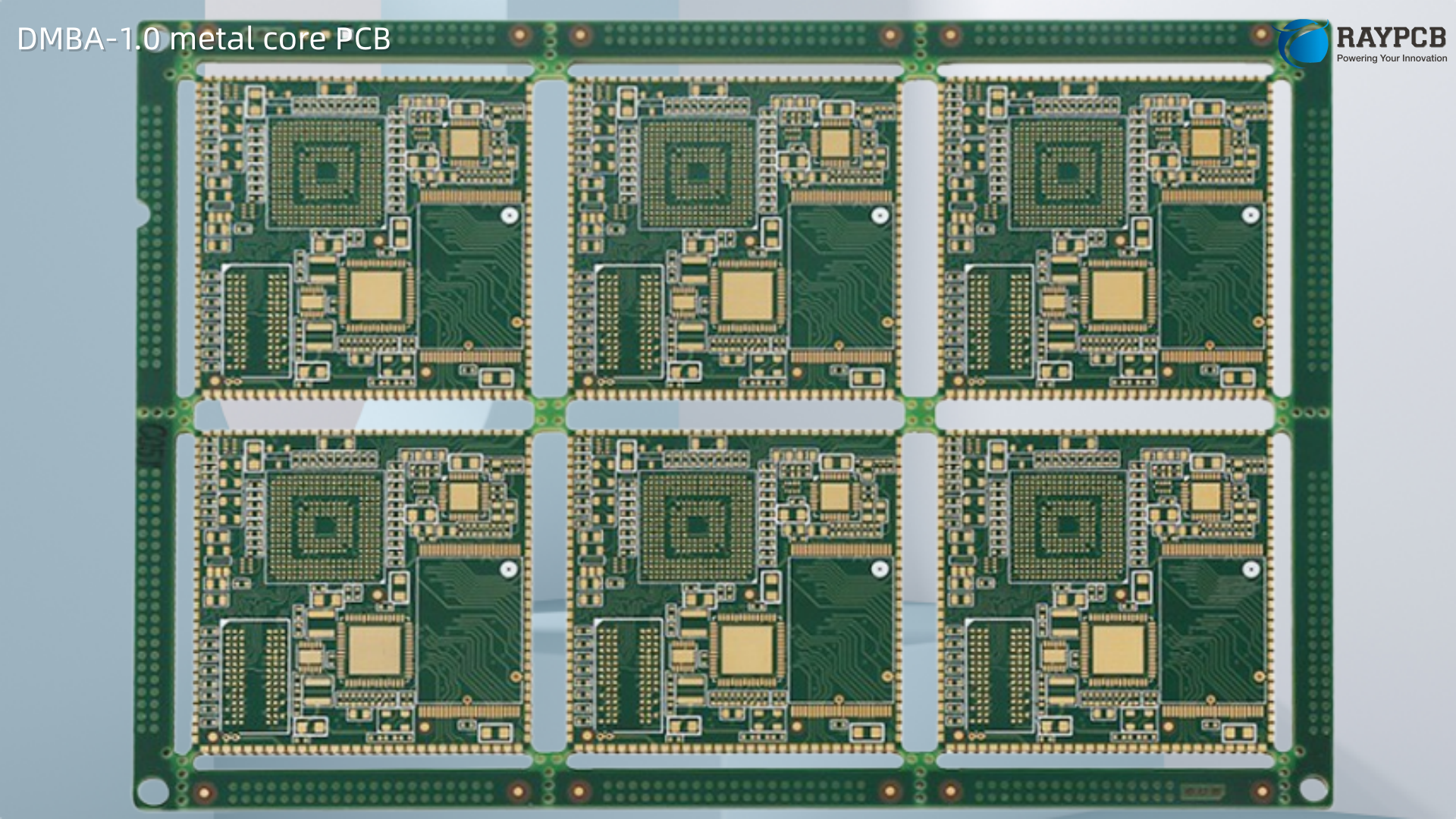
DMBA-1.0 Metal Core PCB Structure and Layer Stack

A standard single-layer DMBA-1.0 MCPCB stack looks like this, from top to bottom:

LayerMaterialTypical Thickness
Solder MaskWhite (LED) or Green15โ€“25 ยตm
Copper CircuitElectrodeposited Cu35 ยตm (1 oz) to 105 ยตm (3 oz)
DMBA-1.0 DielectricCeramic-filled polymer75โ€“130 ยตm
Aluminum BaseAl 1050 / 5052 / 60611.0 mm, 1.6 mm, or 2.0 mm

For LED applications, white solder mask is standard โ€” it improves light reflectivity above 85%, a meaningful gain in luminous efficiency for cavity lighting designs.

If you’re working with Doosan PCB materials or equivalent laminate systems, the DMBA-style dielectric classification maps closely to their standard aluminum IMS product grades. Doosan Electro-Materials has long used vertical integration โ€” from resin synthesis to finished laminate โ€” to maintain consistent dielectric properties, which matters when you’re trying to hit repeatable thermal performance across production runs.

When to Choose DMBA-1.0 โ€” and When to Upgrade

From a practical engineering standpoint, DMBA-1.0 is the right dielectric when:

Use DMBA-1.0 when:

  • LED power per device is 1 W to 3 W
  • Ambient temperature stays below 50ยฐC
  • Board-level junction temperature target is โ‰ค 100ยฐC
  • Cost is a significant design constraint
  • Application is commercial lighting, audio amplifiers, low-power converters, or general industrial control

Consider upgrading beyond 1.0 W/mยทK when:

  • Power density exceeds 5 W per cmยฒ of PCB surface
  • Automotive under-hood environments push ambient above 85ยฐC
  • Your thermal simulation shows dielectric R_th as a dominant term
  • You’re using COB (chip-on-board) configurations requiring tighter thermal margins

A lot of engineers over-specify the dielectric grade on straightforward LED jobs. If your junction temperature budget passes with DMBA-1.0, using a 3.0 W/mยทK dielectric gains you maybe 10โ€“15ยฐC at added material cost and sometimes longer lead times. Run the simulation first.

Design Tips for Getting the Most Out of DMBA-1.0

Minimize Dielectric Thickness Without Sacrificing Isolation

Thinner dielectric = lower thermal resistance, as shown above. Request 75โ€“100 ยตm dielectric thickness when your isolation voltage requirement allows. For most 12 V or 24 V LED systems, this is well within safe margins. Only push to 130 ยตm or above if you’re targeting 3,000 V+ hipot specifications.

Use Thermal Vias Strategically

On multilayer or double-sided configurations, thermal vias connecting top copper pads down toward the metal base improve heat spreading. Use non-conductive epoxy fill to prevent shorting through the base. For single-layer DMBA-1.0 boards, components mounted directly above the aluminum core with minimal dielectric gap get the best thermal path.

Match Your Aluminum Alloy to the Application

Not all aluminum bases behave the same under vibration or high-cycle thermal stress:

AlloyThermal ConductivityBest For
1050 / 1100~230 W/mยทKGeneral LED lighting (cost-optimized)
5052~138 W/mยทKPower supply boards, good corrosion resistance
6061~167 W/mยทKVibration environments (automotive, industrial)

5052 is the most common default for commercial LED MCPCBs using DMBA-1.0 โ€” good balance of thermal performance, machinability, and mechanical strength.

Surface Finish Selection

Surface FinishRecommended Use with DMBA-1.0
HASL (Lead-free)General LED boards, cost-sensitive production
ENIGWire bonding, fine-pitch components, high-reliability
OSPShort shelf-life assemblies, cost reduction
Immersion SilverGood flatness, moderate shelf life

ENIG is the go-to for any LED board where thermal pad flatness matters for tight LED packages.

Common Applications of DMBA-1.0 Metal Core PCB

DMBA-1.0 metal core PCBs are found in a wider range of products than most engineers initially expect. The 1.0 W/mยทK thermal tier handles the thermal load in most commercial-grade applications without the cost penalty of premium dielectrics:

  • LED street lighting and area lightingย โ€” the dominant use case globally
  • Commercial LED downlights and panel lightsย โ€” high-volume, cost-sensitive
  • LED driver power supply boardsย โ€” moderate power dissipation from MOSFETs
  • Automotive interior lightingย โ€” non-underhood applications
  • Consumer audio amplifiersย โ€” power stage thermal management
  • Industrial relay and sensor boardsย โ€” moderate thermal environments
  • Telecommunications power convertersย โ€” secondary-side rectification stages

Useful Resources for DMBA-1.0 and MCPCB Design

The following databases and references are worth bookmarking for anyone working with DMBA-1.0 metal core PCBs and thermal dielectric selection:

  • IPC-2316ย โ€” Design Guide for Metal Core Boards; the baseline specification document for MCPCB stackup and design rules
  • IPC-TM-650ย โ€” Test Methods Manual for measuring thermal conductivity (Method 2.5.58), peel strength, and dielectric breakdown
  • Doosan Electro-Materials product portalย โ€” datasheets for standard and high-performance IMS laminate grades: www.doosanelectromaterials.com
  • UL Product iQ databaseย โ€” verify UL recognition file numbers for your chosen laminate before design lock: iq.ul.com
  • JEDEC JESD51 seriesย โ€” thermal resistance measurement standards for packaged components mounted on MCPCB
  • Bergquist / Henkel thermal management design guideย โ€” practical IMS design examples including dielectric comparison data
  • Z-zero Z-plannerย โ€” stackup tool with Doosan and other laminate libraries for impedance and thermal modeling: z-zero.com/pcb-materials

Frequently Asked Questions About DMBA-1.0 Metal Core PCB

Q1: Is DMBA-1.0 sufficient for high-power LED applications running at 5W per LED?

At 5W per LED, DMBA-1.0 sits right at the edge depending on your pad geometry and ambient temperature. A 1 cmยฒ thermal pad with 100 ยตm DMBA-1.0 dielectric gives roughly 1ยฐC/W of dielectric thermal resistance. Add the LED’s junction-to-case resistance and your system thermal resistance, and run a full budget. If the numbers are tight, a 2.0 W/mยทK dielectric at the same thickness often buys you the margin you need without a major cost hit.

Q2: Can DMBA-1.0 boards be used in automotive applications?

Yes, for interior automotive lighting and non-underhood electronics, DMBA-1.0 handles the thermal environment well. For underhood applications where ambient temperatures regularly hit 85ยฐC+, evaluate whether the total board temperature stays within the dielectric’s rated operating range. In those cases, a higher-grade dielectric or active cooling is worth considering.

Q3: What’s the breakdown voltage of DMBA-1.0, and is it enough for mains-isolated designs?

A standard DMBA-1.0 dielectric typically clears 2,500 V AC in hipot testing, which meets most IEC 60950 and IEC 61347 requirements for LED driver isolation. If your application requires 3,000 V or higher isolation (some industrial and medical designs), specify a thicker dielectric or a dielectric grade with an explicit higher breakdown rating.

Q4: How does DMBA-1.0 compare to Bergquist or Ventec equivalent products?

The 1.0 W/mยทK thermal grade is a widely adopted industry standard, and most major IMS laminate manufacturers โ€” Bergquist (Sil-Pad series), Ventec (VT-4A1), Iteq, and Doosan โ€” all offer products in this tier with comparable performance. The differences show up in resin systems, shelf life, and process compatibility rather than headline thermal conductivity. Always validate with the manufacturer’s published test data against IPC-TM-650.

Q5: What’s the lead time difference between DMBA-1.0 and higher-grade dielectrics?

DMBA-1.0 is a stock material at most volume MCPCB manufacturers โ€” standard lead times of 5โ€“7 business days for quick-turn prototypes and 15โ€“20 days for production runs are typical. Higher-grade dielectrics (3.0 W/mยทK and above) may extend lead time by 1โ€“2 weeks if the fab needs to source specialty laminate. If you’re on a tight schedule, confirm material availability before finalizing your thermal spec.

Understanding DMBA-1.0 metal core PCB material isn’t just about knowing the number on the spec sheet โ€” it’s about knowing how that 1.0 W/mยทK fits into your full thermal stack and whether your design can live with it. Most of the time, it can. When it can’t, now you know where to look.

DFR Series Flex-Rigid PCB Material: Design Considerations, Specs & Engineer’s Guide

DFR flex-rigid PCB material explained: full specs, bend radius rules, stackup tables, IPC-6013 classification, and design tips from an engineer’s perspective.

If you’ve been tasked with designing a board that needs to fold into a camera assembly, survive thousands of bend cycles in a wearable, or route signals through the hinge of an industrial robot, you’ve already landed on rigid-flex as the answer. The next question is material โ€” and that’s where the DFR flex-rigid PCB material series comes in.

DFR (Doosan Flex-Rigid) is a series of laminate and dielectric materials developed for hybrid rigid-flex construction. Unlike off-the-shelf FR-4, DFR materials are engineered specifically to bridge the mechanical and electrical demands of flex zones and rigid sections within a single integrated board. Getting the material selection right from the start saves you from the worst outcome in rigid-flex engineering: a design that clears simulation, fails flex testing, and goes back to the drawing board at prototype stage.

This guide covers what DFR flex-rigid PCB material is, how it fits into the broader laminate landscape, the design rules that actually matter, and the specs you need to evaluate before committing to a stackup.

What Is DFR Flex-Rigid PCB Material?

DFR series materials are part of Doosan PCB‘s portfolio of specialty laminates, covering the flex-to-rigid transition zone that defines the quality of any rigid-flex board. Doosan Electro-Materials โ€” one of the world’s largest CCL (copper clad laminate) producers, with annual output exceeding 15 million square meters across facilities in Korea, China, and Europe โ€” developed the DFR series to give fabricators a controlled, predictable material system for IPC-6013 Type 4 construction.

At its core, DFR series laminate addresses the hardest problem in rigid-flex design: bonding dissimilar materials without sacrificing performance at the interface. The flex sections use polyimide (PI) substrate with rolled annealed (RA) copper, while the rigid sections use low-flow prepreg and FR-4 or high-Tg polyimide cores. The DFR system governs both the dielectric composition and the bondply behavior at that rigid-to-flex transition.

Why the Transition Zone Is Everything

Most delamination and cracking failures in rigid-flex boards don’t happen in the middle of the flex area โ€” they happen at the boundary where flex meets rigid. That transition zone concentrates mechanical stress, creates CTE mismatch at solder reflow temperatures, and is where adhesive squeeze-out most commonly contaminates the flex zone during lamination. DFR materials are engineered with controlled resin flow properties to minimize these failure modes.

DFR Flex-Rigid PCB Material: Key Specifications

The DFR series spans multiple grades to cover a range of layer counts, thermal requirements, and flex-usage classes per IPC-6013. The following table summarizes the core properties of DFR flex-rigid laminate:

PropertyDFR Standard GradeDFR High-Tg Grade
Base SubstratePolyimide (PI) filmPolyimide (PI) film
Flex Copper TypeRolled Annealed (RA)Rolled Annealed (RA)
Flex Copper Weight1/3 oz, 1/2 oz, 1 oz1/3 oz, 1/2 oz, 1 oz
Polyimide Film Thickness25 ยตm, 50 ยตm, 75 ยตm, 100 ยตm25 ยตm, 50 ยตm, 75 ยตm
Tg (Rigid Prepreg)โ‰ฅ 150ยฐCโ‰ฅ 175ยฐC
Dielectric Constant (Dk)3.4โ€“3.6 @ 1 GHz3.3โ€“3.5 @ 1 GHz
Dissipation Factor (Df)0.010โ€“0.0200.008โ€“0.015
Peel Strength (1 oz Cu)โ‰ฅ 1.0 N/mmโ‰ฅ 1.0 N/mm
FlammabilityUL 94 V-0UL 94 V-0
IPC ClassificationType 4, Class 2/3Type 4, Class 3
Operating Temperature-55ยฐC to +130ยฐC-55ยฐC to +155ยฐC

The high-Tg grade is the better call for automotive underhood, aerospace, and any application where the board sees reflow multiple times during rework.

Understanding the DFR Series Layer Stackup

Rigid-flex stackup design is more complex than standard FR-4. With DFR materials, you’re managing at least three distinct zones: the rigid section, the flex section, and the transition. Each has its own material behavior.

A typical 6-layer DFR rigid-flex stackup (4 rigid layers + 2 flex layers) looks like this:

LayerMaterialThickness
Top Copper (Rigid)1 oz ED Copper35 ยตm
Prepreg (Rigid)Low-flow DFR prepreg100 ยตm
Inner Copper 1 (Rigid+Flex)1/2 oz RA Copper18 ยตm
DFR Polyimide Core (Flex)PI film50 ยตm
Inner Copper 2 (Rigid+Flex)1/2 oz RA Copper18 ยตm
BondplyAcrylic or adhesiveless PI25โ€“50 ยตm
Bottom Copper (Rigid)1 oz ED Copper35 ยตm
Coverlay (Flex Zone)PI film + adhesive25 ยตm PI + 25 ยตm adhesive
Aluminum Base (Optional)Al 1050 or 50521.0โ€“1.6 mm

One thing engineers frequently miss: the bondply used to attach flex cores to rigid sections in DFR construction must be a low-flow or no-flow prepreg. Standard prepreg will bleed resin into the flex zone during lamination, stiffening an area that needs to remain compliant. This contaminates the bend region and is one of the leading causes of field failures on first-time rigid-flex builds.

Critical Design Considerations for DFR Flex-Rigid PCB Material

Bend Radius Rules You Cannot Ignore

Bend radius is the single most important mechanical parameter in any DFR flex-rigid design. Getting this wrong by 20% can cut flex-cycle life from 100,000 cycles down to a few hundred.

Per IPC-2223 and industry practice, the minimum bend radius for DFR polyimide-based flex sections follows:

Flex Layer CountMinimum Bend RadiusUsage
1-layer flex6ร— total flex thicknessFlex-to-install (static)
2-layer flex10ร— total flex thicknessFlex-to-install (static)
2-layer flex20ร— total flex thicknessDynamic flex (repeated bending)
3+ layer flex12ร— total flex thicknessFlex-to-install (static)
3+ layer flex24ร— total flex thicknessDynamic flex

For a 2-layer DFR flex section with 50 ยตm PI and 18 ยตm copper per layer, total flex thickness is approximately 200 ยตm including coverlay. Your minimum static bend radius would be 2.0 mm. For a dynamic application like a foldable device hinge, that jumps to 4.0 mm. Many designers try to push below these limits to save space โ€” in DFR materials, this reliably creates micro-cracks in the RA copper that propagate over thermal cycling.

Rolled Annealed vs. Electrodeposited Copper in Flex Zones

This is a material choice that has a direct, measurable impact on flex-cycle life. DFR series flex zones use rolled annealed (RA) copper exclusively, and for good reason:

Copper TypeGrain StructureFlex Cycles (Typical)Signal Loss at High Frequency
Rolled Annealed (RA)Elongated, parallel to surface100,000โ€“1,000,000+Lower (smoother surface)
Electrodeposited (ED)Columnar, perpendicular500โ€“5,000Higher

RA copper’s molecular grain structure runs parallel to the bending plane, allowing it to flex without crack initiation at grain boundaries. ED copper โ€” which is fine for rigid sections โ€” will develop micro-cracks in the flex zone after relatively few cycles. DFR specifies RA copper for all flex layers, but double-check this with your fabricator, especially on hybrid stackups where ED copper may be used on outer rigid layers for cost reasons.

Coverlay vs. Liquid Photoimageable Solder Mask in Flex Zones

This matters more than most engineers initially realize. Standard LPI (liquid photoimageable) solder mask is brittle. When applied to a DFR flex zone, it cracks after minimal bending โ€” sometimes before the board even leaves the factory. In DFR flex-rigid design:

Use coverlay in all flex zones. Coverlay is a laminated polyimide film with acrylic adhesive โ€” it flexes with the circuit and maintains adhesion through repeated bending cycles. Reserve LPI solder mask for rigid sections only.

A 25 ยตm polyimide coverlay with 25 ยตm adhesive is the standard specification for DFR flex zones. For tighter bend radii or higher cycle counts, a 12.5 ยตm PI film with adhesiveless bonding offers better compliance.

Symmetrical Stackup Is Not Optional

An unbalanced copper distribution in DFR rigid-flex boards creates bow and twist after lamination โ€” sometimes severe enough to fail IPC-6013 flatness requirements on the rigid sections. Copper weight and layer count must be mirrored around the neutral axis of the flex stack. This is especially important in multilayer DFR designs where the rigid section has more copper layers than the flex.

If your design demands asymmetric copper loading โ€” as often happens in power/signal mixed-layer count designs โ€” discuss pre-compensation with your fab before releasing artwork. Most experienced rigid-flex fabricators will add copper balancing layers or adjust prepreg thickness to compensate.

DFR Flex-Rigid PCB Material in High-Speed Applications

Polyimide has a natural advantage over FR-4 for high-frequency signals: lower dielectric constant (Dk ~3.4 vs. ~4.5 for FR-4) and smoother copper surface (RA copper). The DFR series leverages both properties to maintain controlled impedance across the rigid-to-flex transition.

For USB 3.x, PCIe, and other differential pair protocols through a DFR flex zone, the key design parameters are:

Signal StandardTarget ImpedanceTypical DFR Trace WidthSpacing
USB 3.190 ฮฉ differential~120โ€“150 ยตm150 ยตm
PCIe Gen 3/485 ฮฉ differential~130โ€“160 ยตm160 ยตm
LVDS100 ฮฉ differential~110โ€“140 ยตm140 ยตm
Microstrip (single-ended)50 ฮฉ~160โ€“220 ยตmโ€”

Note that trace widths for a given impedance target will differ in the flex zone vs. rigid zone because the dielectric thickness and material properties change. Your impedance calculator needs to account for this at every zone boundary โ€” a common oversight that produces impedance discontinuities right at the transition, exactly where you least want them.

IPC-6013 Classification for DFR Flex-Rigid Boards

DFR series builds are classified under IPC-6013, which is the specific performance specification for flexible and rigid-flex printed circuit boards (not IPC-6012, which covers rigid-only boards).

IPC-6013 ClassApplication LevelDFR Grade Recommendation
Class 1General consumerStandard DFR, lower cycle count
Class 2Industrial, commercialStandard DFR, โ‰ฅ IPC-2223 compliance
Class 3High-reliability (medical, aerospace, automotive)High-Tg DFR, IPC-6013E Rev. E

For medical devices, defense, and aerospace, Class 3 is the baseline โ€” not an upgrade. Class 3 requires stricter plating thickness, tighter registration tolerances, and documented bend testing with cycle logs. DFR high-Tg laminate is the correct material specification for Class 3 builds.

Common Applications of DFR Flex-Rigid PCB Material

DFR series materials show up in applications where the board itself needs to perform a mechanical function, not just route signals:

  • Wearables and medical devicesย โ€” compact form factors, body-contoured assemblies, implantables
  • Aerospace and defenseย โ€” avionics harnesses, guided missile systems, cockpit display modules
  • Consumer cameras and dronesย โ€” lens actuator boards, gimbal assemblies
  • Automotiveย โ€” dashboard modules, ADAS camera/radar connectors, EV battery management
  • Industrial roboticsย โ€” joint-following circuits in robot arm assemblies
  • Foldable smartphones and laptopsย โ€” hinge region interconnects requiring millions of bend cycles

Useful Resources for DFR Flex-Rigid PCB Design

Bookmark these references before you finalize any DFR rigid-flex design:

  • IPC-2223Cย โ€” Design Standard for Flexible/Rigid-Flexible Printed Boards (governs bend radius, stiffeners, and stackup): ipc.org
  • IPC-6013Eย (Rev. September 2021) โ€” Qualification and Performance Specification for Flexible/Rigid-Flexible Printed Boards; the fabrication performance standard
  • IPC-4101ย โ€” Specification for Base Materials for Rigid/Multilayer Printed Boards (covers prepreg and laminate slash sheets used in DFR rigid sections)
  • Doosan Electro-Materials product portalย โ€” DFR and polyimide laminate datasheets: doosanelectromaterials.com
  • DuPont Pyraluxยฎ Design Guideย โ€” industry-standard flex material design reference covering PI film grades, RA copper specs, and bend radius calculations: dupont.com/pyralux
  • Altium Designer Rigid-Flex PCB Guideย โ€” free software documentation for 3D rigid-flex stackup definition: altium.com
  • Z-zero Z-plannerย โ€” impedance stackup tool with Doosan and polyimide laminate libraries: z-zero.com/pcb-materials
  • IPC-A-600ย โ€” Acceptability of Printed Boards (visual acceptance criteria used alongside IPC-6013 for inspection)

Frequently Asked Questions About DFR Flex-Rigid PCB Material

Q1: Can DFR flex-rigid boards be wave soldered?

Not recommended for the flex sections. Wave soldering exposes the board to a continuous thermal load that stresses the PI-to-rigid transition zone and can cause adhesive creep or delamination at the bondply. DFR rigid-flex assemblies are typically processed through SMT reflow on the rigid sections only, with manual or selective solder for any through-hole components in rigid areas. The flex sections should never enter the wave solder bath.

Q2: What’s the maximum layer count for a DFR rigid-flex build?

DFR materials support up to 22 layers total (typically up to 10 flex layers within that stack), with blind and buried vias possible in the rigid sections. Beyond 12โ€“14 total layers, sequential lamination passes are required, which significantly increase cost and lead time. Most practical DFR designs run 4โ€“10 layers total.

Q3: How does DFR flex-rigid material compare to DuPont Pyralux in terms of performance?

Both are polyimide-based flex-rigid laminate systems with comparable Dk, Df, and temperature ratings. Pyralux AP and Pyralux APR are the industry benchmark for adhesiveless flex laminate in high-reliability applications. DFR materials are competitive in terms of electrical and thermal performance and offer a cost advantage in Asian supply chains. For Class 3 medical or aerospace builds where UL and MIL qualification documentation is critical, confirm that your specific DFR grade carries the necessary recognition files before committing.

Q4: Do DFR flex zones require stiffeners?

Stiffeners are needed anywhere a flex zone must support a connector, heavy component, or ZIF (zero insertion force) contact area. Typical DFR stiffener materials are FR-4 (0.2โ€“1.0 mm) bonded with PSA (pressure-sensitive adhesive) or PI stiffener with thermally cured epoxy. Place stiffeners on the rigid side of the board structure, not inside the flex zone โ€” stiffeners in the flex zone effectively turn it into a rigid zone and can cause stress concentration at the stiffener edge.

Q5: What is the typical lead time for DFR flex-rigid PCBs versus standard FR-4?

DFR rigid-flex builds run 15โ€“25 business days for production quantities, versus 5โ€“10 days for standard FR-4. Quick-turn prototypes are typically 10โ€“15 days. The extended lead time reflects the additional lamination cycles, controlled-depth routing to reveal flex zones, and mandatory bend testing for Class 2/3 builds. If your schedule is tight, lock in the DFR material grade and stackup with your fabricator early โ€” rigid-flex jobs that hit DFM issues at the fab stage routinely lose 5โ€“10 days to stackup revisions.

DFR flex-rigid PCB material gives you the freedom to design in three dimensions โ€” but that freedom comes with tighter constraints on bend radius, material balance, and lamination control than any rigid board. Get the stackup right at the start, and DFR delivers boards that survive conditions FR-4 simply cannot handle.

DE-175 High Tg Laminate: 175ยฐC Glass Transition Temperature for High-Reliability PCBs

DE-175 high Tg laminate: 175ยฐC Tg, T260 >60 min, โ‰ค3% Z-CTE. Full specs, IPC-4101/99 guide, automotive & multilayer PCB engineering tips.

There’s a class of PCB designs that standard FR-4 simply cannot support โ€” not because standard FR-4 is a bad material, but because 130โ€“135ยฐC Tg was never designed for lead-free assembly, 20-layer backplanes, automotive underhood environments, or anything that sees repeated 260ยฐC thermal excursions. That’s where the DE-175 high Tg laminate sits: a multifunctional epoxy-glass laminate engineered for thermal robustness, dimensional stability, and long service life in conditions that would age or delaminate ordinary substrates within a few years.

This guide covers what separates DE-175 from both standard FR-4 and from premium low-loss laminates, what its properties actually mean for your design, and how to deploy it correctly in high-reliability builds.

What Makes a 175ยฐC Tg Laminate Different from Standard FR-4

Before getting into DE-175 specifics, it’s worth grounding the Tg discussion in something engineers can calculate against. Tg โ€” glass transition temperature โ€” is the point at which the epoxy resin matrix transitions from a rigid, glassy state to a softer, rubbery state. Above that threshold, the laminate’s Z-axis coefficient of thermal expansion (CTE) increases sharply, mechanical properties degrade, and dimensional stability drops.

Standard FR-4 at 130โ€“135ยฐC Tg was qualified in an era of eutectic tin-lead soldering, where peak reflow temperatures stayed around 183ยฐC. Lead-free SAC305 alloy changed that picture: peak reflow now runs 245โ€“260ยฐC, meaning the laminate sees temperatures nearly 130ยฐC above its Tg during every assembly cycle. For thin single-layer boards with no vias, that’s tolerable. For a 16-layer telecom backplane or an automotive ECU going through multiple reflow cycles plus field thermal cycling, it’s a reliability liability.

The industry standard guidance is that your laminate’s Tg should be at least 10โ€“20ยฐC above the maximum continuous operating temperature, and your Td (decomposition temperature) should be well above your peak process temperature. A DE-175 high Tg laminate at 175ยฐC Tg covers most industrial, automotive, and server-class designs comfortably.

DE-175 High Tg Laminate: Full Technical Specifications

The following table consolidates the key properties of the DE-175 175ยฐC Tg laminate class. These values are consistent with IPC-4101 slash sheet /26 and /126 requirements for high-Tg multifunctional epoxy laminates:

PropertyTest MethodTypical Value
Glass Transition Temperature (Tg)DSC โ€” IPC-TM-650 2.4.25โ‰ฅ 175ยฐC
Decomposition Temperature (Td)TGA 5% weight loss โ€” 2.4.24.6โ‰ฅ 340ยฐC
Time to Delaminate (T260)TMA โ€” IPC-TM-650 2.4.24.1> 60 minutes
Time to Delaminate (T288)TMA โ€” IPC-TM-650 2.4.24.1> 20 minutes
Z-Axis CTE (50โ€“260ยฐC, total)IPC-TM-650 2.4.24Cโ‰ค 3.0%
Z-Axis CTE (pre-Tg)IPC-TM-650 2.4.24C~50 ppm/ยฐC
X/Y-Axis CTE (pre-Tg)IPC-TM-650 2.4.24C14โ€“16 ppm/ยฐC
Dk @ 1 GHzIPC-TM-650 2.5.5.9~4.1โ€“4.4
Df @ 1 GHzIPC-TM-650 2.5.5.9~0.015โ€“0.020
Dk @ 10 GHzIPC-TM-650 2.5.5.5~4.0โ€“4.2
Df @ 10 GHzIPC-TM-650 2.5.5.5~0.016โ€“0.022
Moisture AbsorptionIPC-TM-650 2.6.2.1Aโ‰ค 0.30%
Flexural Strength (length direction)IPC-TM-650 2.4.4Bโ‰ฅ 415 MPa
Peel Strength (1 oz copper, after thermal stress)IPC-TM-650 2.4.8Cโ‰ฅ 0.9 N/mm
CAF Resistance85ยฐC/85%RH, 50V DCโ‰ฅ 1000 hours
Thermal ConductivityASTM E1952~0.30โ€“0.36 W/mยทK
FlammabilityUL 94V-0
IPC-4101 Slash Sheetโ€”/26 or /126
RoHS ComplianceEU 2011/65/EUYes

The T260 > 60 minutes figure is one of the most operationally meaningful numbers in that table. It tells you the laminate can survive an hour at 260ยฐC โ€” equivalent to lead-free reflow temperatures โ€” before delamination begins. That’s the margin that makes double-sided assembly plus rework feasible without delamination risk.

Understanding the Tg 175ยฐC Threshold in Practice

Why 175ยฐC Is the Sweet Spot for Lead-Free High-Reliability Design

The 175ยฐC Tg tier hits the right balance for a wide range of demanding applications. Here’s why the math works out:

Lead-free peak reflow at 260ยฐC represents an 85ยฐC overshoot above Tg for a 175ยฐC material. That sounds like a lot, but the key parameter isn’t Tg alone โ€” it’s the T260/T288 time-to-delamination performance. A well-formulated 175ยฐC Tg resin with T260 > 60 minutes can survive this exposure far better than a poorly formulated 185ยฐC Tg resin with T260 < 5 minutes.

Post-reflow, when the board returns to operating temperature โ€” say, an automotive ECU that sees 125ยฐC ambient continuously โ€” a 175ยฐC Tg material is operating with a 50ยฐC margin below Tg. Compare that to a 135ยฐC Tg material operating at the same 125ยฐC: only 10ยฐC of margin, deep into the CTE transition zone. That difference in daily operating margin is what separates five-year failure-free field life from field returns.

Z-Axis CTE and Via Reliability: The Real Failure Mode

High-Tg materials at 170ยฐC and above are required for lead-free assembly with multiple reflow cycles, thick boards over 2 mm where via stress is higher, and automotive applications with operating temperatures up to 125ยฐC per AEC-Q standards.

For DE-175, the Z-axis CTE of approximately 50 ppm/ยฐC pre-Tg (compared to 70โ€“80 ppm/ยฐC for standard FR-4) directly translates to reduced barrel stress on plated through-holes during thermal cycling. When you’re designing a 20-layer backplane with 0.25 mm finished hole diameters and aspect ratios of 10:1 or higher, that CTE difference between a standard FR-4 and a 175ยฐC Tg material is the difference between 10-year PTH reliability and early barrel cracking at thermal cycle 500.

DE-175 High Tg Laminate vs. Competing High-Tg Materials

Here’s how DE-175 positions against commonly evaluated alternatives in the 170โ€“185ยฐC Tg tier:

MaterialManufacturerTg (ยฐC)Td (ยฐC)T260Dk @ 1GHzDf @ 1GHzKey Differentiator
DE-175โ€”175โ‰ฅ 340> 60 min~4.2~0.018Mid-tier high-Tg, broad applicability
IT-180AITEQ175> 340> 60 min~4.1~0.016Low Df, CAF tested, server/auto
KB-6167Kingboard175โ‰ฅ 340> 60 min4.50.016Cost-competitive, automotive
TU-768TUC175โ‰ฅ 340> 60 min~4.5~0.021Halogen-free option available
370HRIsola180340> 60 min4.040.021Best CAF track record, spread weave
185HRIsola180/18534060 min~4.0~0.020AOI fluorescence, aerospace
S1000-2Shengyi175โ‰ฅ 340> 30 min4.60.020High-volume Asia fab supply

The DE-175 fits into a widely populated but important material tier. What differentiates specific product choices within this tier often comes down to your fab house’s process experience, pricing, regional availability, and whether you need specific certifications (e.g., automotive IATF 16949 supply chain documentation, or UL File Numbers for end-product certification).

Where DE-175 High Tg Laminate Excels

Multilayer Boards With 8+ Layers

The combination of โ‰ค 3.0% Z-axis total expansion and T260 > 60 minutes makes DE-175 appropriate for any multilayer design where sequential lamination, blind/buried vias, or high aspect-ratio through-holes create demanding thermal stress scenarios. A 12-layer server logic board going through four reflow/soldering cycles needs exactly this kind of thermal headroom.

Automotive Electronics โ€” Body and Chassis Applications

In automotive electronics, high-Tg PCBs are widely used in on-board computers, engine control units (ECUs), sensors, dashboards, and other critical systems. The interior of a car experiences significant temperature fluctuations, so circuit board materials capable of withstanding high temperatures and thermal stress are needed.

The 175ยฐC Tg with โ‰ฅ 1000-hour CAF resistance covers the vast majority of automotive PCB applications outside of direct powertrain modules. For body control modules, HVAC controllers, instrument clusters, and ADAS baseband processing boards, DE-175 provides the reliability margin required by OEM qualification programs without requiring exotic polyimide substrates.

Industrial Control and Power Electronics

Motor drives, servo controllers, inverter gate driver boards, and PLC CPU modules all generate significant internal heat while operating in non-climate-controlled enclosures. Industrial PLCs often run 24/7 in non-climate-controlled enclosures. The combination of continuous internal heat generation and long service life demands materials that resist thermal aging. The 50ยฐC operating margin that a DE-175 board provides above 125ยฐC ambient is what enables 10โ€“15 year field MTBF in these environments.

Telecom Infrastructure and Server Hardware

Backplanes, line cards, and routing switch fabrics operate in thermally dense environments with high layer counts. The spread-weave glass fabric options available for 175ยฐC Tg laminates also help with fiber-weave skew on differential pairs, which becomes relevant for 10/25GbE and PCIe Gen 4/5 signal routing.

Medical Equipment Requiring Sterilization Tolerance

Autoclaved medical instrumentation PCBs see steam sterilization cycles at 121โ€“134ยฐC โ€” an environment where standard FR-4 would show progressive degradation. DE-175’s Tg provides more than 40ยฐC of margin above sterilization temperatures, and its low moisture absorption (โ‰ค 0.30%) limits Dk drift in high-humidity operating environments like operating theaters and ICU equipment.

IPC-4101 Slash Sheet Classification for DE-175

Understanding which IPC-4101 slash sheet your design requires is important for procurement and qualification:

IPC-4101 Slash SheetTg RequirementUse Case
/21Not specified (standard FR-4)Consumer, low-complexity
/26Tg โ‰ฅ 150ยฐC (epoxy, non-filled)Mid-Tg lead-free
/126Tg โ‰ฅ 150ยฐC (epoxy, filled)High-reliability mid-Tg
/99Tg โ‰ฅ 170ยฐC (high-performance multifunctional epoxy)High-Tg multilayer

DE-175 at 175ยฐC Tg qualifies under /99 as a high-performance multifunctional epoxy laminate. When writing your PCB fab notes or purchase spec, specifying “IPC-4101 slash /99, Tg โ‰ฅ 175ยฐC” is the correct way to establish the material class requirement without locking a single brand.

CAF Resistance: Why It Matters More Than You Think

Conductive Anodic Filament (CAF) failure is an electrochemical phenomenon that engineers underestimate until they see a field return with an intermittent short in a board that visually looks perfect. CAF forms when copper ions migrate along the glass-resin interface, driven by voltage bias in the presence of moisture. In dense via fields โ€” especially after any drilling-induced glass-resin bond damage โ€” CAF is a real long-term failure mode.

DE-175 class materials use multifunctional epoxy resin systems with better cross-link density than standard FR-4. That denser polymer network, combined with more controlled glass sizing chemistry, produces glass-resin interfaces with fewer voids and migration pathways. The โ‰ฅ 1000-hour CAF resistance rating (85ยฐC/85%RH at 50V DC) is the qualification metric you want to confirm on the actual datasheet of whatever specific DE-175-class product you’re sourcing.

If you’re using Doosan PCB laminates and selecting within their high-Tg epoxy family, cross-reference their published CAF data against this threshold โ€” some products publish 1000-hour data at 100V bias, which represents a tougher qualification than the 50V standard.

Processing Guidelines for DE-175 High Tg Laminate

Drilling

High-Tg multifunctional epoxy resins are typically harder and more brittle than standard FR-4 due to their denser cross-link network. Use fresh or recently resharpened drill bits โ€” wear that would be acceptable for standard FR-4 will cause more smear and microcracking on 175ยฐC Tg material. Reduce feed rate by approximately 10โ€“15% compared to your standard FR-4 baseline for the same diameter and aspect ratio.

Desmear Process

The higher cross-link density that gives DE-175 its thermal robustness also means resin smear in drilled holes is harder to remove. Your fab house needs a calibrated permanganate desmear process tuned for high-Tg material โ€” not just the same recipe used for standard FR-4. Inadequate desmear is one of the leading causes of CAF failure in otherwise well-designed high-Tg boards. Worth a specific conversation with your CM before first article.

Lamination Parameters

High-Tg FR-4 often requires longer cure times to achieve full cross-linking of the epoxy. Press temperatures typically run 170โ€“185ยฐC for 175ยฐC Tg systems, with extended cure dwell compared to standard FR-4. Your laminate supplier’s processing guide will have the specific press cycle for their resin system โ€” follow it rather than defaulting to your standard FR-4 program.

Pre-bake Before Layup

Store panels in sealed moisture barrier bags at 20โ€“25ยฐC, below 50% RH. If panels have been exposed to ambient conditions for more than 5โ€“7 days, pre-bake at 120ยฐC for 2โ€“4 hours before layup. Moisture absorbed into a high-Tg prepreg creates steam pockets during lamination that show up as measling or blistering on thermal stress test.

Surface Finishes

DE-175 is compatible with all standard surface finishes: ENIG, ENEPIG, OSP, immersion silver, immersion tin, and lead-free HASL. For high-reliability applications where the board may see multiple rework cycles, ENIG or ENEPIG is preferred over OSP or immersion tin due to superior solderability shelf life.

Dk/Df Frequency Behavior and Signal Integrity Context

FrequencyDk (Typical)Df (Typical)
100 MHz4.40โ€“4.500.013โ€“0.016
500 MHz4.30โ€“4.450.015โ€“0.018
1 GHz4.10โ€“4.400.015โ€“0.020
5 GHz4.00โ€“4.300.016โ€“0.022
10 GHz4.00โ€“4.200.018โ€“0.024

The Df range for DE-175-class materials at 10 GHz is notably better than standard FR-4 (which typically runs Df 0.025โ€“0.030 at 10 GHz), though it still trails purpose-built low-loss materials like Isola FR408HR (Df ~0.009) or Rogers RO4350B (Df ~0.0037).

For the majority of DE-175 applications โ€” server switch fabrics at 25G, automotive ADAS baseband at 5โ€“8 GHz, telecom line cards running PCIe Gen 5 backplane traces โ€” the Df performance is more than adequate. If your channel budget analysis shows you need Df below 0.010 at 10 GHz, you’re in a different material tier.

Useful Resources for DE-175 High Tg Laminate

ResourceDescriptionLink
IPC-4101E StandardBase materials specification โ€” slash /99 for high-Tgipc.org
IPC-TM-650 Test MethodsAll laminate property test proceduresipc.org/TM-650
ITEQ IT-180A DatasheetReal 175ยฐC Tg reference laminate specsiteq.com.tw
Kingboard KB-6167 Datasheet175ยฐC Tg automotive-qualified laminatekingboard.com
Isola 370HR Product PageIndustry benchmark 180ยฐC Tg comparisonisola-group.com
TUC TU-768 DatasheetHalogen-free 175ยฐC Tg optiontuc.com.tw
Doosan PCB MaterialsHigh-Tg laminate options for multilayer designsDoosan PCB
UL Product iQVerify UL flammability and thermal certificationiq.ul.com
EU RoHS Directive 2011/65/EURestricted substance compliance referenceec.europa.eu

5 FAQs About DE-175 High Tg Laminate

Q1: My current design uses standard FR-4 at 135ยฐC Tg. Do I really need to upgrade to DE-175 for a 12-layer lead-free assembly board? Almost certainly yes, if the board will see double-sided reflow plus any rework. Standard 135ยฐC Tg has essentially no Tg margin over lead-free reflow temperatures, and its T260/T288 time-to-delamination is typically under 5 minutes. For a 12-layer board with buried vias, delamination between any inner pair during a rework event is a real risk. DE-175 gives you T260 > 60 minutes โ€” that’s 12x the thermal dwell margin at the same temperature. The cost delta on the raw laminate is typically 15โ€“25% over standard FR-4, which is negligible against board fabrication costs.

Q2: What’s the difference between IPC-4101/26 and /99, and which applies to DE-175? Slash /26 covers standard epoxy systems with Tg โ‰ฅ 150ยฐC โ€” this includes a lot of “mid-Tg” materials. Slash /99 is specifically for high-performance multifunctional epoxy systems with Tg โ‰ฅ 170ยฐC. DE-175 at 175ยฐC Tg falls under /99. When specifying on your fab drawing, use “IPC-4101 /99” to clearly communicate that you require a true high-performance high-Tg material, not just any material that technically passes the /26 Tg floor.

Q3: Can DE-175 be used in a hybrid stackup alongside a lower-loss material like FR408HR? Yes, hybrid stackups are common for designs that need both thermal reliability and low signal loss on specific layers. The critical parameter to verify is CTE compatibility between the two materials โ€” you need similar X/Y-axis CTE (typically 13โ€“16 ppm/ยฐC pre-Tg) to avoid registration drift and interlaminar stress during lamination. Also confirm that the press cycle for both materials is compatible โ€” your fabricator needs to run a single cure cycle that works for both resin systems. Get explicit confirmation from your fab house before committing a hybrid stackup design to production.

Q4: How does DE-175 perform in Highly Accelerated Life Testing (HALT) for automotive qualification? For HALT profiles up to 130ยฐC operating temperature (typical AEC-Q200 Class IV), DE-175 provides a comfortable 45ยฐC Tg margin. For extended temperature range profiles reaching 150ยฐC, you’re getting close to the Tg boundary and should consider whether a 185โ€“200ยฐC Tg material is more appropriate for the specific test profile. The โ‰ฅ 1000-hour CAF resistance at 85ยฐC/85%RH is generally sufficient for body electronics qualification, but powertrain boards with direct heat exposure may require additional testing to the specific OEM’s internal qualification standard.

Q5: Is DE-175 suitable for HDI boards with laser-drilled microvias? Yes. The 175ยฐC Tg system is compatible with laser drilling for microvia formation โ€” the resin chemistry ablates cleanly under COโ‚‚ or UV laser. The key processing consideration is that the denser resin may require slightly adjusted laser parameters compared to standard FR-4. Low Z-axis CTE is also beneficial for HDI: stacked and staggered microvia structures put stress on the dielectric between microvia pads during thermal cycling, and the lower expansion coefficient of a 175ยฐC Tg material reduces that stress over the product lifetime.

Engineering Decision Framework: When to Specify DE-175

The following decision criteria summarize when upgrading to DE-175 high Tg laminate is justified:

Design ConditionRecommendation
Layer count โ‰ฅ 8 layersDE-175 or higher โ€” low Z-CTE critical
Lead-free assembly with double-sided reflowDE-175 minimum
Operating temperature โ‰ฅ 100ยฐC continuousDE-175 minimum
Automotive ECU (body/chassis)DE-175 appropriate
Via aspect ratio โ‰ฅ 8:1DE-175 or higher for barrel reliability
Sequential lamination (HDI)DE-175 appropriate
Telecom backplane / server bladeDE-175 appropriate
Operating temperature โ‰ฅ 150ยฐC continuousConsider 185โ€“200ยฐC Tg or polyimide
Signal loss critical above 10 GHzConsider low-loss laminate instead
Simple 4-layer consumer board, Tg 135ยฐC is fineStandard FR-4 sufficient

Final Thoughts

The DE-175 high Tg laminate class represents a well-defined, well-proven tier of PCB substrate performance. Engineers who have been burned by standard FR-4 delamination on complex multilayer boards know exactly why this tier exists. The 40ยฐC improvement in Tg over standard FR-4, combined with the dramatic improvements in T260/T288, Z-axis CTE, and CAF resistance, translates directly into boards that survive lead-free assembly without issue and then operate reliably through the product’s intended service life.

The engineering case for specifying 175ยฐC Tg materials is straightforward for any design that combines high layer count, lead-free assembly, and operating temperatures above 85ยฐC. The additional cost is low, the process compatibility with standard FR-4 fabrication lines is high, and the reliability gain is measurable. When your next 12-layer industrial or automotive board enters layout, DE-175 belongs in your default material stack.

DE-150HF: Halogen-Free High Tg Material for Lead-Free Processes

A complete engineering guide to DE-150HF halogen-free laminate โ€” covering key specs (Tg โ‰ฅ150ยฐC, Td โ‰ฅ340ยฐC), how it meets IEC 61249-2-21, comparison vs. standard FR-4, fabrication tips, application fit, and 5 FAQs for PCB designers.

There’s a moment in every PCB material selection conversation when two requirements collide head-on: the thermal demands of lead-free soldering and the environmental mandate to eliminate halogens. For years, engineers treated these as a trade-off โ€” you could get reliable lead-free performance, or you could satisfy your customer’s halogen-free requirements, but optimizing both simultaneously meant paying a steep premium. DE-150HF halogen-free laminate sits in the product category designed to close that gap, delivering a Tg of โ‰ฅ150ยฐC alongside full IEC 61249-2-21 halogen-free compliance at a price point that makes sense for mainstream industrial and consumer designs.

If you’re evaluating this material for a new design or trying to understand where it fits relative to standard FR-4 and higher-performance alternatives, this guide covers the full picture โ€” from raw specifications to processing considerations to real-world application fit.

What Is DE-150HF Halogen-Free Laminate?

DE-150HF is a glass-fiber-reinforced, modified epoxy copper-clad laminate (CCL) formulated without brominated or chlorinated flame retardants. The “HF” suffix is the important differentiator: it signals that the flame retardancy mechanism is achieved through phosphorus-based or nitrogen-based chemistry rather than the halogenated compounds used in conventional FR-4.

The “150” in the designation refers to the target glass transition temperature โ€” โ‰ฅ150ยฐC measured by DSC โ€” which places this material firmly in the enhanced-thermal category above standard FR-4 (typically 130โ€“140ยฐC) but below ultra-high-Tg grades targeting 170โ€“180ยฐC. That 150ยฐC threshold is a practical sweet spot for many lead-free designs: it provides meaningful margin over standard FR-4 while keeping material cost and process complexity lower than full high-Tg grades.

Within the broader Doosan PCB material ecosystem, DE-150HF represents the convergence of two important trends that have reshaped laminate selection over the past decade โ€” the shift to lead-free assembly driven by RoHS, and the parallel push toward halogen-free materials driven by environmental regulations and OEM sustainability mandates.

The Regulatory Context: Why DE-150HF Halogen-Free Matters

Understanding why a material like DE-150HF exists requires understanding the regulatory environment that created demand for it.

For a PCB to meet halogen-free classification under IEC 61249-2-21 and RoHS guidelines, it must contain less than 900 ppm of chlorine or bromine individually, and less than 1,500 ppm total halogens. These thresholds are the hard limits that define whether a material qualifies for halogen-free certification.

Traditional FR-4 flame retardancy relies heavily on tetrabromobisphenol-A (TBBPA), a brominated compound that is highly effective but generates toxic byproducts โ€” dioxins and furans โ€” when burned or incinerated. Halogen-free materials eliminate this risk at the source, significantly reducing the negative environmental impact of electronics throughout their lifecycle.

The performance benefit of eliminating halogens goes beyond environmental compliance. Halogen replacement tends to raise the molecular weight and Tg value of the resin system, resulting in improved thermal stability. The material molecules move less when heated than regular epoxy boards do, which results in a lower CTE value that helps the board structure stay intact even under temperature changes.

This is the core value proposition of DE-150HF halogen-free: you’re not giving up thermal performance to achieve environmental compliance. You’re getting both simultaneously.

DE-150HF Key Technical Specifications

The property profile below reflects the DE-150HF halogen-free laminate platform, tested per standard IPC test methods:

PropertyTest MethodDE-150HF Value
Glass Transition Temperature (Tg)DSC โ€“ IPC-TM-650 2.4.25โ‰ฅ 150ยฐC
Thermal Decomposition Temp (Td)TGA โ€“ IPC-TM-650 2.4.40โ‰ฅ 340ยฐC
T-288 (Time to Delamination)TMA โ€“ IPC-TM-650 2.4.24.1> 5 min
T-300 (Time to Delamination)TMA โ€“ IPC-TM-650 2.4.24.1> 1 min
Z-axis CTE (50โ€“260ยฐC)TMAโ‰ค 3.5%
Dielectric Constant (Dk) at 1 GHzIPC-TM-650 2.5.5~4.0โ€“4.2
Dissipation Factor (Df) at 1 GHzIPC-TM-650 2.5.5~0.012โ€“0.015
Peel Strength (1 oz Cu, Condition A)IPC-TM-650 2.4.8โ‰ฅ 1.5 N/mm
Water AbsorptionIPC-TM-650 2.6.2โ‰ค 0.10%
FlammabilityUL 94V-0
Halogen Content (Cl/Br)IEC 61249-2-21< 900 ppm each
Total Halogen ContentIEC 61249-2-21< 1,500 ppm

The Td โ‰ฅ 340ยฐC figure is worth pausing on. For high-reliability applications, materials with a Td above 340ยฐC are recommended to withstand soldering and operational heat. DE-150HF meets this threshold, which means the resin won’t begin chemically decomposing during lead-free peak reflow temperatures (245โ€“260ยฐC) โ€” a failure mode that can produce blistering, outgassing, and permanent delamination.

DE-150HF Halogen-Free vs. Standard FR-4: The Practical Comparison

A lot of engineers ask the same question at this stage: is the upgrade from standard FR-4 to DE-150HF halogen-free actually justified for their application? Here’s the numbers-based answer:

ParameterStandard FR-4 (Tg ~135ยฐC)DE-150HF Halogen-Free
Tg (DSC)130โ€“140ยฐCโ‰ฅ 150ยฐC
Td~300โ€“310ยฐCโ‰ฅ 340ยฐC
Halogen-Free CertifiedNoYes (IEC 61249-2-21)
Z-axis CTE (50โ€“260ยฐC)~4.0โ€“4.5%โ‰ค 3.5%
Water Absorption0.13โ€“0.15%โ‰ค 0.10%
Lead-Free Process FitMarginal (single pass)Yes (multiple passes)
Toxic Combustion ProductsDioxins/furans possibleSignificantly reduced
Typical Cost PremiumBaseline~10โ€“20%

The lower water absorption in DE-150HF halogen-free is a real-world reliability factor that doesn’t always get the attention it deserves. Some halogen-free materials show a moisture absorption rate of less than 0.1%, compared to 0.2% for traditional options, reducing the risk of delamination in humid environments. For boards deployed in industrial or outdoor environments, this difference accumulates meaningfully over product service life.

Why DE-150HF Halogen-Free Is the Right Choice for Lead-Free Assembly

The fundamental issue with standard FR-4 in lead-free processes comes down to the Tg gap. During the 240ยฐCโ€“270ยฐC lead-free reflow soldering process, normal Tg PCBs usually lose 1.5% to 3% of resin weight. The lost resin weight may reduce PCB reliability or even lead to soldering defects. Even if visual inspection passes, the micro-structural degradation accumulates across multiple thermal cycles.

DE-150HF halogen-free addresses this through two mechanisms working together:

Higher Tg margin โ€” With Tg โ‰ฅ 150ยฐC, the resin is further from its softening point during lead-free reflow. The matrix stays more rigid, z-axis expansion is more controlled, and barrel stress on plated through-holes is lower.

Phosphorus-based flame retardant chemistry โ€” The P/N-based resin systems used in halogen-free laminates inherently form a denser polymer network than brominated systems. The content of nitrogen and phosphorus in halogen-free PCB is higher than that of halogen in common halogen-based materials, so its monomer molecular weight and Tg value have increased. When heated, its molecular mobility will be lower than that of conventional epoxy resin, so the thermal expansion coefficient of halogen-free PCB material is relatively small.

This isn’t a coincidence โ€” it’s the chemistry working in your favor on both the regulatory and performance fronts simultaneously.

Applications Where DE-150HF Halogen-Free Delivers Real Value

Application SectorSpecific Use CasesWhy DE-150HF Fits
Consumer ElectronicsSmartphones, tablets, laptops, IoT devicesOEM halogen-free mandates, lead-free assembly, thin multilayer builds
Automotive ElectronicsECU, ADAS sensors, infotainmentThermal cycling, moisture resistance, RoHS + halogen-free compliance
Industrial ControlPLCs, motor drives, HMI displaysLong service life, multi-reflow compatibility
Medical DevicesMonitoring equipment, diagnosticsLow water absorption, chemical resistance, regulatory compliance
TelecommunicationsSmall cell equipment, access pointsMultiple reflow cycles, halogen-free OEM mandates
Power ElectronicsDC-DC converters, UPS boardsSustained thermal stress, halogen-free certification

It’s worth noting that halogen-free mandates, CTI requirements for power electronics, and flammability ratings all influence material selection in these sectors โ€” and DE-150HF addresses all three in a single material specification.

Understanding the Flame Retardancy Mechanism in DE-150HF Halogen-Free

One concern engineers occasionally raise is whether halogen-free materials provide adequate flame retardancy without brominated compounds. It’s a fair question, and the answer requires understanding the mechanism difference.

Halogenated flame retardants work through a gas-phase mechanism: halogen radicals interrupt the combustion chain reaction in the vapor above the burning surface. Phosphorus-based systems โ€” like those used in DE-150HF halogen-free โ€” work through a condensed-phase mechanism: they promote char formation on the material surface during combustion, physically blocking oxygen and heat transfer to the underlying material.

The end result โ€” UL 94 V-0 classification โ€” is identical. The combustion byproducts are dramatically different. Phosphorus-char systems do not produce the dioxins and furans associated with brominated flame retardants during incineration or soldering operations.

Halogen-free FR-4 eliminates bromine- and chlorine-based flame retardants, which can produce toxic gases when burned. Flame retardancy is achieved through phosphorus- or nitrogen-based compounds instead of halogens. For operators working near reflow ovens and for end-of-life recycling processes, this is a meaningful safety improvement.

Fabrication Guidelines for DE-150HF Halogen-Free Laminate

Processing DE-150HF halogen-free on standard FR-4 equipment is achievable, but several parameters need adjustment from your standard FR-4 baseline.

Drilling Considerations

Halogen-free PCBs increase the molecular weight and the rigidity of molecular bonds by using P and N series functional groups, thus enhancing the rigidity of materials. At the same time, the Tg point of halogen-free materials is generally higher than that of ordinary copper clad laminate. Therefore, the drilling effect of ordinary FR-4 drilling parameters is generally not ideal. Reduce feed rate slightly on thicker cores and monitor bit wear more frequently than you would with standard FR-4.

Etching and Chemical Processes

Generally, the alkali resistance of halogen-free PCB is worse than that of common FR-4. Therefore, special attention should be paid to the etching process and the rework process after solder resist, and the soaking time in alkaline stripping solution should not be too long, so as to prevent white spots on the substrate. Build shorter dwell times into your alkaline process steps and verify with first-article inspection before committing to full production runs.

Lamination

Halogen-free resin systems may require modified press cure profiles compared to standard brominated FR-4. Check the material supplier’s processing guide for temperature, pressure, and dwell time recommendations. Using a standard FR-4 cure cycle risks under-curing the resin, which compromises Tg performance โ€” the exact thing you paid for when upgrading to DE-150HF.

Pre-Assembly Moisture Bake

DE-150HF halogen-free has excellent low water absorption (โ‰ค 0.10%), but pre-assembly baking at 120ยฐC for 2โ€“4 hours is still recommended, particularly for boards that have been stored in humid conditions or shipped internationally. This eliminates any absorbed moisture that could cause steam-induced delamination during lead-free reflow.

DE-150HF Halogen-Free Compared to Competing Materials

MaterialManufacturerTg (DSC)TdHalogen-FreeKey Differentiator
DE-150HFโ€”โ‰ฅ 150ยฐCโ‰ฅ 340ยฐCYesCost-effective HF + enhanced Tg
IT-150GIteqโ‰ฅ 150ยฐCโ‰ฅ 340ยฐCYesTaiwan fab availability
S1155Shengyiโ‰ฅ 150ยฐCโ‰ฅ 335ยฐCYesHigh-volume Chinese supply chain
TU-768TUCโ‰ฅ 170ยฐCโ‰ฅ 340ยฐCYesHigher Tg step up
370HRIsolaโ‰ฅ 180ยฐCโ‰ฅ 340ยฐCYesNorth America premium segment
R-1566WPanasonicโ‰ฅ 150ยฐCโ‰ฅ 340ยฐCYesJapanese automotive OEM trust

DE-150HF halogen-free competes in the mainstream cost-performance segment โ€” positioned above commodity standard FR-4 but below the premium high-Tg materials required for the most demanding multilayer designs.

Useful Resources for PCB Engineers and Procurement Teams

  • IEC 61249-2-21ย โ€” The defining international standard for halogen-free base materials used in PCBs, specifying the <900 ppm Cl/Br threshold: https://www.iec.ch
  • IPC-4101Eย โ€” IPC specification for base materials for rigid and multilayer PCBs, including classification of halogen-free grades: https://www.ipc.org
  • IPC-TM-650 Test Methods Manualย โ€” Defines all standard laminate test procedures including Tg (DSC), Td (TGA), T-288, CTE, and peel strength: https://www.ipc.org/TM
  • RoHS Directive 2011/65/EUย โ€” The EU regulation that underpins industry-wide lead-free and hazardous substance restrictions: https://ec.europa.eu/environment/topics/waste-and-recycling/rohs-directive
  • UL Product iQย โ€” Verify UL 94 flammability certifications for specific laminate products: https://iq.ul.com
  • JPCA-ES-01ย โ€” Japanese standard for halogen-free PCB materials, often cross-referenced for products targeting Japanese OEM customers: https://www.jpca.net
  • IPC J-STD-020ย โ€” Moisture/reflow sensitivity classification for SMD packages, directly relevant to understanding why laminate thermal performance matters during assembly: https://www.ipc.org

Frequently Asked Questions About DE-150HF Halogen-Free Laminate

Q1: Is Tg 150ยฐC sufficient for lead-free SAC305 reflow assembly?

Yes, with appropriate process control. Lead-free SAC305 peaks at 245โ€“260ยฐC, which is well above any laminate’s Tg including DE-150HF. What Tg determines is how gracefully the material handles that thermal stress โ€” specifically, how much z-axis expansion occurs and how quickly the material recovers below Tg. A Tg of โ‰ฅ150ยฐC provides meaningful improvement over standard FR-4 (130โ€“140ยฐC Tg), reducing barrel fatigue risk on through-holes and delamination risk on multilayer builds. For designs requiring more than 4 reflow passes, consider stepping up to a โ‰ฅ170ยฐC Tg grade.

Q2: Does DE-150HF halogen-free cost significantly more than standard FR-4?

Typically 10โ€“20% more at material level. The gap has narrowed considerably as halogen-free laminate production has scaled up over the past decade. The total cost delta on a finished PCB is smaller still โ€” laminate material represents only a fraction of total board cost. For most designs where halogen-free compliance is required, the specification adds minimal cost compared to the market access and regulatory risk of non-compliance.

Q3: Can DE-150HF halogen-free be processed on the same equipment as standard FR-4?

Yes, the same drill presses, lamination presses, plating lines, and imaging equipment apply. The key adjustments are: slower drill feed rates on thick cores, shorter alkaline chemistry dwell times, and a modified lamination cure profile per the material supplier’s processing guide. Run a qualification panel before full production and inspect hole wall quality, inner-layer adhesion, and peel strength as your primary pass/fail criteria.

Q4: How does DE-150HF halogen-free achieve UL 94 V-0 without bromine?

Through phosphorus-based and/or nitrogen-based flame retardant chemistry. Phosphorus compounds work by promoting char formation on the material surface during combustion, which physically excludes oxygen and slows flame propagation. The resulting UL 94 V-0 classification is the same as brominated FR-4 โ€” the difference is in what combustion byproducts are generated, not in the fire performance rating itself. This is verified through UL testing on each qualified material grade.

Q5: What IPC-4101E slash sheet applies to DE-150HF halogen-free?

DE-150HF with Tg โ‰ฅ150ยฐC and halogen-free certification typically maps to IPC-4101E /94 (halogen-free, enhanced thermal FR-4 epoxy, Tg โ‰ฅ 150ยฐC by DSC). Some variants may map to /121 depending on specific resin type and filler system. Confirm the exact slash sheet with your laminate supplier’s technical documentation before writing procurement specs or fab notes. When specifying to your PCB fabricator, include explicit language: “Halogen-free per IEC 61249-2-21, Tg โ‰ฅ 150ยฐC DSC” to prevent substitution with non-compliant material.

Final Engineering Perspective

DE-150HF halogen-free laminate occupies an important and growing segment of the PCB materials market โ€” the crossover point where lead-free thermal requirements and halogen-free environmental requirements meet at an accessible price point. It’s not the right answer for every design: if your application requires 6+ reflow cycles or operates continuously at elevated temperatures, a โ‰ฅ170ยฐC Tg grade is the more appropriate choice. But for the large population of designs that need reliable lead-free assembly performance, full IEC 61249-2-21 halogen-free certification, and a cost structure that doesn’t blow up the BOM, DE-150HF halogen-free hits all three requirements without compromise.

In a regulatory environment where halogen-free is increasingly a table-stakes market access requirement rather than a premium option, materials like DE-150HF aren’t just environmentally responsible choices โ€” they’re practically inevitable ones.

Suggested Meta Description:

A complete engineering guide to DE-150HF halogen-free laminate โ€” covering key specs (Tg โ‰ฅ150ยฐC, Td โ‰ฅ340ยฐC), how it meets IEC 61249-2-21, comparison vs. standard FR-4, fabrication tips, application fit, and 5 FAQs for PCB designers.

DE-150 Laminate: High Thermal Stability for Demanding Environments

DE-150 PCB laminate guide โ€” full thermal specs (Tg 150ยฐC, Td 330ยฐC), lead-free reflow compatibility, industrial & automotive applications, fabrication tips, competitor comparison, and 5 engineer FAQs.

There’s a common pattern in PCB material selection that leads to expensive mistakes: engineers default to standard FR-4 (Tg ~130โ€“140ยฐC) until the first field return comes back with delaminated layers or cracked via barrels โ€” and only then start looking for something better. DE-150 PCB laminate sits in exactly the right gap to prevent that problem. With a glass transition temperature targeting 150ยฐC and a thermal profile designed for lead-free assembly and continuous duty operation, it addresses the most common reasons mid-range industrial and automotive boards fail thermally.

This guide covers what DE-150 laminate brings to the table, how its specs compare against similar-class materials, where it earns its keep in real applications, and what fabricators need to know before running it through production.

What Is DE-150 PCB Laminate?

DE-150 is a mid-Tg epoxy-based copper clad laminate (CCL) engineered for applications where standard FR-4 hits its thermal limits but where the cost and processing requirements of very high-Tg or specialty materials (polyimide, PTFE) aren’t justified. The “150” in the designation signals its Tg classification: approximately 150ยฐC measured by DSC or TMA โ€” putting it firmly in the mid-Tg category that IPC-4101 categorizes under slash sheets like /124 (unfilled, mid-Tg) or /129 (halogen-free variants).

The resin system is a multifunctional or modified epoxy formulation that delivers better thermal decomposition resistance than standard FR-4 while maintaining compatibility with conventional PCB fabrication processes โ€” drilling, lamination chemistry, surface finish options, and solder mask adhesion all stay within the standard FR-4 envelope. That’s a meaningful advantage over some exotic alternatives: you don’t need new press programs or retrained process engineers to run DE-150 in an established shop.

In terms of chemistry, DE-150 class laminates typically use a dicy-free or low-dicy hardener system that contributes directly to improved CAF resistance and better moisture stability โ€” both real-world failure modes that standard FR-4 struggles with in high-humidity industrial environments.

DE-150 PCB Laminate: Technical Specifications

The specifications below represent typical DE-150 class performance. As with all laminates, always verify exact values against the current revision of the manufacturer’s datasheet โ€” production batch variations and copper foil weight affect certain properties.

Thermal Properties

PropertyTypical ValueTest Method
Glass Transition Temperature (Tg)โ‰ฅ 150ยฐCDSC / IPC-TM-650 2.4.25
Decomposition Temperature (Td)โ‰ฅ 330ยฐC (5% weight loss)TGA
T-260 (Time to Delamination)> 30 minIPC-TM-650 2.4.24.1
T-288 (Time to Delamination)> 5 minIPC-TM-650 2.4.24.1
CTE Z-axis (ฮฑ1, below Tg)50โ€“60 ppm/ยฐCTMA
CTE Z-axis (ฮฑ2, above Tg)200โ€“250 ppm/ยฐCTMA
CTE X/Y axis14โ€“17 ppm/ยฐCTMA
Max Operating Temp (UL 796)130ยฐCโ€”

The Td of โ‰ฅ 330ยฐC gives meaningful margin over standard FR-4 (Td typically ~300ยฐC) for lead-free reflow at 260ยฐC peak. That 70ยฐC buffer above peak reflow temperature is what prevents the resin from beginning to chemically decompose during multi-pass assembly.

Electrical Properties

PropertyTypical ValueFrequency / Condition
Dielectric Constant (Dk)4.3 โ€“ 4.71 GHz
Dissipation Factor (Df)0.018 โ€“ 0.0221 GHz
Volume Resistivityโ‰ฅ 10โธ MฮฉยทcmC-96/35/90
Surface Resistivityโ‰ฅ 10โถ MฮฉC-96/35/90
Dielectric Breakdown Voltageโ‰ฅ 40 kV/mmโ€”
CTI (Comparative Tracking Index)โ‰ฅ 175 Vโ€”

The Dk in the 4.3โ€“4.7 range is consistent with the mid-Tg FR-4 family โ€” not ideal for RF work, but perfectly serviceable for digital, power, and mixed-signal designs operating below 3โ€“4 GHz where the signal integrity budget isn’t razor-thin.

Mechanical Properties

PropertyTypical ValueTest Standard
Flexural Strength (lengthwise)โ‰ฅ 415 MPaIPC-TM-650 2.4.4
Flexural Strength (crosswise)โ‰ฅ 345 MPaIPC-TM-650 2.4.4
Peel Strength (1 oz Cu, after thermal stress)โ‰ฅ 0.90 N/mmIPC-TM-650 2.4.8
Water Absorptionโ‰ค 0.20%D-24/23
Dimensional Stabilityโ‰ค 0.10% (X/Y)IPC-TM-650 2.4.39

Compliance & Certification

AttributeStatus
UL Flammability Rating94 V-0
RoHS ComplianceYes
Lead-Free Assembly CompatibleYes
IPC-4101 Slash Sheet/124 (unfilled mid-Tg)

Why Mid-Tg Matters: The Engineering Case for DE-150

Understanding where DE-150 PCB laminate sits in the material hierarchy helps calibrate when it’s the right call and when it isn’t.

Material ClassTg RangeTypical Use CaseLead-Free Compatible?
Standard FR-4130โ€“140ยฐCConsumer electronics, low-power designsMarginal
Mid-Tg FR-4 (DE-150 class)148โ€“165ยฐCIndustrial, automotive, telecomYes
High-Tg FR-4170โ€“185ยฐCHigh-reliability automotive, server boardsYes
Polyimideโ‰ฅ 250ยฐCAerospace, military, flex PCBsYes
PTFE/Low-lossVariesRF, microwave, 5GYes

The argument for DE-150 in industrial and moderate-duty automotive applications is straightforward: standard FR-4 boards running lead-free assembly already experience multiple 260ยฐC peak excursions during reflow, and standard FR-4 (Tg 130โ€“140ยฐC) begins operating above its glass transition temperature during soldering. That results in Z-axis expansion that stresses plated through-holes, particularly in thick multilayer boards. DE-150’s 150ยฐC Tg keeps the resin in its glassy state during more of the assembly process, reducing barrel cracking and delamination risk significantly.

DE-150 PCB Laminate Applications: Where It Works Best

Industrial Power Electronics and Motor Drives

Variable frequency drives, motor controllers, and power supply units run continuously at elevated case temperatures. The combination of thermal endurance above standard FR-4, good Z-axis CTE, and lead-free compatibility makes DE-150 a natural fit. In these designs, PCB operating temperature can easily sit at 100โ€“120ยฐC during continuous duty โ€” that 20โ€“30ยฐC margin below the Tg is exactly the buffer IPC and most automotive OEMs recommend.

Automotive Control Modules (Non-Under-Hood)

For cabin-mounted and HVAC control modules, door control units, and body electronics โ€” where ambient temperatures reach 85โ€“105ยฐC but don’t approach the extremes of under-hood placement โ€” DE-150 hits the right performance-cost balance. Under-hood applications targeting continuous 125โ€“150ยฐC should step up to high-Tg materials like DS-7409 or equivalent 170ยฐC+ laminates.

Telecom Infrastructure

Outdoor base station boards, repeater electronics, and junction box PCBs in telecommunications infrastructure see temperature extremes from direct sun exposure, condensation cycling, and prolonged operation. DE-150’s improved moisture resistance (โ‰ค 0.20% water absorption) and thermal stability extend mean time between failures in these continuous-duty environments.

Industrial Automation and PLC Boards

Programmable logic controllers and industrial I/O boards installed adjacent to heat-producing process equipment benefit from DE-150’s improved heat resistance. In factory automation environments where the electrical cabinet itself runs at 60โ€“85ยฐC ambient, the extra thermal headroom is not academic โ€” it’s the difference between a 5-year service life and a 12-year one.

Multilayer Boards with High Via Density

For any multilayer design with more than 12 layers, or with through-hole pitches below 0.8 mm, Z-axis CTE management is critical. DE-150’s lower Z-axis expansion compared to standard FR-4 reduces via barrel fatigue over thermal cycling, which is the most common root cause of latent multilayer board failures in field-deployed industrial equipment.

Processing DE-150 PCB Laminate: Fabricator Notes

One of DE-150’s strongest selling points is that it processes essentially like standard FR-4. That said, a few parameters deserve attention:

Lamination: Standard press cycles with peak temperatures of 170โ€“185ยฐC work well. The mid-Tg resin system needs adequate cure time above 170ยฐC (minimum 45โ€“60 minutes is typical) to fully develop its Tg. Rushing the cure produces under-cured resin that won’t achieve rated Tg โ€” a common quality escape in shops switching from faster-cure standard FR-4.

Drilling: No special geometry required. Drill hit count recommendations are standard FR-4 class โ€” maintain appropriate entry material for fine-drill work. The material is slightly harder than standard FR-4 due to the modified resin, so expect modestly higher drill wear in high-volume production and plan stack heights accordingly.

Lead-Free Reflow: DE-150 handles SAC305 reflow at 260ยฐC peak. For boards requiring three or more reflow passes (double-sided SMT plus rework allowance), verify T-288 data with the specific material lot. The typical T-288 > 5 min means careful rework timing on the third pass.

Storage: Store in original sealed packaging in a cool, dry environment below 23ยฐC and 50% RH. Bake at 120ยฐC for 2โ€“4 hours before lamination if panels have been stored beyond 6 months or exposed to elevated humidity.

Useful Resources for DE-150 PCB Laminate

Engineers evaluating DE-150 PCB laminate alongside competing options will find these resources directly useful:

  • Manufacturer Datasheetย โ€” Always the primary reference. Verify current revision and lot-specific property ranges. Request directly from your laminate distributor or fabricator.
  • IPC-4101E Standardย โ€” Governing specification for rigid PCB base materials; mid-Tg halogen-free variants align with /124 (unfilled) or /129 (halogen-free) slash sheets.
  • IPC-TM-650 Test Method Manualย โ€” Reference document for understanding how Tg, Td, T-260/T-288, CTE, and peel strength are measured and what the numbers actually mean.
  • UL Product iQ (iq.ul.com)ย โ€” Verify current UL 94 V-0 fire safety certification, applicable copper weights, and construction approvals.
  • IPC-2221Bย โ€” Generic PCB design standard; Section 8 provides direct guidance on material class selection relative to thermal and environmental requirements.
  • RayPCB Doosan PCB Materials Guideย โ€” Helpful reference for comparing mid-Tg laminates across product families: Doosan PCB
  • IPC-9151 (Comparative Tracking Index)ย โ€” Useful if your application has high-voltage creepage requirements; CTI values above 175V (DE-150 typical) determine pollution degree suitability.

5 FAQs About DE-150 PCB Laminate

Q1: Is DE-150 suitable for lead-free assembly without any process modifications?

Yes โ€” this is the core reason mid-Tg laminates like DE-150 exist. The combination of Tg โ‰ฅ 150ยฐC and Td โ‰ฅ 330ยฐC provides adequate margin for SAC305 reflow at 260ยฐC peak. Standard FR-4 (Tg 130โ€“140ยฐC) is operating above its own glass transition temperature during lead-free reflow, which is why via barrel cracking and delamination are significantly more common on standard FR-4 boards assembled with lead-free processes. DE-150 eliminates this structural risk without requiring press cycle changes.

Q2: What’s the practical difference between DE-150 (Tg 150ยฐC) and high-Tg materials at 170ยฐC for a typical industrial board?

Roughly 20ยฐC of additional thermal headroom in operation and greater delamination resistance through extended thermal stress tests (T-260, T-288). For boards with operating temperatures below 120ยฐC and moderate thermal cycling requirements, DE-150 is generally sufficient and costs less. For heavy-duty automotive (under-hood), server infrastructure, or military-grade applications with operating temperatures consistently above 125ยฐC or requiring IPC Class 3 reliability standards, stepping up to a 170ยฐC+ laminate makes engineering sense.

Q3: How does DE-150’s moisture resistance compare to standard FR-4?

Measurably better. Mid-Tg laminates in the DE-150 class typically achieve water absorption โ‰ค 0.20% vs. standard FR-4 which can run 0.25โ€“0.35%. In practice, lower moisture absorption reduces the risk of delamination during reflow (steam-induced delamination โ€” colloquially called “popcorning” โ€” requires adequate moisture content), and maintains more consistent dielectric properties in humid environments. For outdoor or marine-adjacent deployments, this is a real reliability advantage.

Q4: Can DE-150 laminate be used in hybrid stackups with low-loss or RF materials?

Yes, but hybrid lamination requires planning. The CTE compatibility between DE-150 and low-loss materials (Rogers RO4350B, Isola 370HR, etc.) should be evaluated layer by layer, particularly Z-axis CTE. Many fabricators have established hybrid press parameters for common combinations. Discuss the hybrid intent with your fabricator before design is locked โ€” hybrid stackups are manageable but require material compatibility confirmation upfront.

Q5: What should I check on a DE-150 datasheet before approving it for a new design?

Three items that engineers often overlook: First, verify the T-260 and T-288 values โ€” the delamination time data, not just the Tg. A material can have a Tg of 150ยฐC but poor time-to-delamination, which matters more for multiple reflow passes. Second, check the Z-axis CTE both below and above Tg (ฮฑ1 and ฮฑ2) โ€” the ratio and absolute values determine via reliability in thick boards. Third, confirm that the UL 94 V-0 recognition covers your specific copper weight and thickness combination, as UL recognition is construction-specific, not blanket-certified for all configurations.

Closing Perspective

DE-150 PCB laminate occupies a well-earned middle ground in the laminate selection hierarchy. It isn’t a specialty material โ€” it doesn’t command the price premium or processing complexity of high-Tg, polyimide, or low-loss laminates. What it does is eliminate the most common thermal failure modes that occur when standard FR-4 is pushed into lead-free assembly or continuous industrial duty: delamination, via barrel fatigue, and dielectric instability from moisture uptake.

For the wide band of applications that runs between “consumer electronics with standard FR-4” and “automotive under-hood or aerospace with 170ยฐC+ polyimide” โ€” industrial controls, telecom peripherals, moderate-duty automotive modules, power electronics โ€” DE-150 is often exactly the right material at exactly the right price. The engineering principle is simple: you always want at least 20โ€“25ยฐC of margin between your laminate’s Tg and your worst-case operating temperature. DE-150 gives you that margin where standard FR-4 doesn’t, without the cost and process overhead of going further than you need.

Meta Description Suggestions

Full version (192 characters):

DE-150 PCB laminate guide โ€” full thermal specs (Tg 150ยฐC, Td 330ยฐC), lead-free reflow compatibility, industrial & automotive applications, fabrication tips, competitor comparison, and 5 engineer FAQs.

Yoast-green version (157 characters โ€” recommended):

DE-150 PCB laminate specs, datasheet guide & applications. Mid-Tg laminate for industrial, automotive & telecom PCBs. Thermal properties, tables & FAQs included.

DE-104 PCB Material: Specs, RF Performance, and Real-World Engineering Guide

DE-104 PCB material from Isola: Tg 135ยฐC, Dk 4.37 @ 1GHz, railway EN 45545-2 approved. Full specs, Df tables, competitor comparison & engineering guide.

If your project sits in that common middle ground โ€” not a simple consumer gadget running at DC, but not a 10 GHz mmWave radar module either โ€” there’s a good chance the DE-104 PCB material from Isola Group deserves a spot in your laminate shortlist. It’s one of those workhorses that never gets glamorous press coverage, but shows up in automotive electronics, industrial controls, medical instrumentation, and consumer products by the millions.

This guide breaks down every property that matters, where this material actually makes sense versus where you’d be leaving performance on the table, and how it compares to some common alternatives engineers evaluate at the same time.

What Is DE-104 PCB Material?

DE-104 is a low-Tg copper-clad laminate and prepreg system manufactured by Isola Group, one of the oldest and most recognized names in PCB substrate materials (founded 1912). It is classified as FR-4 under NEMA grades and meets the requirements of IPC-4101 slash sheet /21, the standard specification for epoxy/woven-glass base materials.

Despite the “low Tg” classification, DE-104 has a special resin system that delivers notably better thermal resistance than plain commodity FR-4 โ€” particularly in Z-axis CTE control and decomposition temperature. It’s manufactured in Isola’s European facility, which matters for supply chain qualification in some regulated sectors like railway and medical.

The product is available in both laminate (core) and prepreg form, covering a thickness range from 0.05 mm to 2.4 mm, making it usable across single-layer, double-sided, and complex multilayer stackups.

DE-104 PCB Material: Full Technical Specifications

Here’s the complete property table you’d pull when running a material qualification assessment:

PropertyCondition / Test MethodTypical Value
Glass Transition Temp (Tg)DSC โ€” IPC-TM-650 2.4.25C135ยฐC
Decomposition Temp (Td)TGA 5% weight loss โ€” 2.4.24.6315ยฐC
Time to Delaminate (T260)TMA, copper removed โ€” 2.4.24.112 minutes
Z-Axis CTE (50โ€“260ยฐC)IPC-TM-650 2.4.24C4.2% total
Z-Axis CTE (pre-Tg)IPC-TM-650 2.4.24C70 ppm/ยฐC
X/Y-Axis CTE (pre-Tg)IPC-TM-650 2.4.24C16 / 13 ppm/ยฐC
Thermal ConductivityASTM E19520.36 W/mยทK
Dk @ 1 GHzIPC-TM-650 2.5.5.94.37
Df @ 1 GHzIPC-TM-650 2.5.5.90.022
Dk @ 5 GHzIPC-TM-650 2.5.5.54.32
Df @ 5 GHzIPC-TM-650 2.5.5.50.024
Dielectric BreakdownIPC-TM-650 2.5.6B>50 kV
Arc ResistanceIPC-TM-650 2.5.1B105 seconds
Moisture AbsorptionIPC-TM-650 2.6.2.1A0.3%
Flexural Strength (length)IPC-TM-650 2.4.4B579 MPa
Flexural Strength (cross)IPC-TM-650 2.4.4B450 MPa
Peel Strength (after thermal stress)IPC-TM-650 2.4.8C1.58 N/mm
FlammabilityUL 94V-0
Relative Thermal Index (RTI)UL 94130ยฐC
RoHS ComplianceEU 2011/65/EUYes

UL File Number: E41625. IPC-4101 slash sheet: /21.

Understanding DE-104’s Dk/Df Across Frequency

This is where it gets interesting for engineers doing any kind of controlled-impedance or sub-5 GHz signal routing. DE-104’s dielectric properties shift predictably with frequency, which is typical of epoxy-glass systems:

FrequencyDk (Permittivity)Df (Loss Tangent)
100 MHz4.460.020
500 MHz4.400.021
1 GHz4.370.022
2 GHz4.350.023
5 GHz4.320.024

The Dk variation from 100 MHz to 5 GHz is only about 3.1%, which is actually quite good consistency for an epoxy/glass system. This frequency-stable behavior means your impedance calculations hold up reasonably well from DC to the lower end of the microwave band.

The Df of 0.022โ€“0.024 up to 5 GHz puts it firmly in the “usable but not optimized for RF” zone. For comparison, Rogers RO4350B hits Df of ~0.0037 at 10 GHz. If your signal path insertion loss budget is tight at 3โ€“5 GHz, you’ll feel the difference. But for many industrial and consumer applications running sub-2 GHz interfaces โ€” think Zigbee, Sub-GHz IoT, LPWAN, lower-band LTE modules, or CAN bus systems โ€” DE-104’s loss profile is entirely acceptable.

Prepreg Constructions and Resin Content

One of the practical advantages of DE-104 for multilayer design is the range of prepreg constructions available. Resin content directly affects both Dk/Df and bondline thickness, so having options matters when you’re targeting specific impedance in a dense stackup.

Glass StyleResin ContentThickness (mm)Dk @ 1 GHzDf @ 1 GHz
10673%0.0584.020.024
108064%0.0774.180.022
211354%0.1004.370.020
211650%0.1204.450.019
762845%0.1984.560.018

The higher resin content in fine-weave styles like 106 and 1080 yields lower Dk values โ€” useful when you need thinner dielectrics with tighter impedance control on outer signal layers. The 7628 glass with lower resin content gives you a stiffer mechanical construction better suited for core layers carrying power planes.

DE-104 vs. Competing FR-4 Class Laminates

Here’s how DE-104 stacks up against materials engineers commonly evaluate in the same application tier:

MaterialManufacturerTg (ยฐC)Td (ยฐC)Dk @ 1GHzDf @ 1GHzNotable Difference
DE-104Isola1353154.370.022Railway EN 45545-2 approved
IS400Isola1353104.400.021Standard commodity FR-4
IT-180AIteq1803404.400.021Higher Tg for lead-free intensive
FR408Isola1853703.690.012Low-loss, next tier up
TU-768TUC1753404.600.021Halogen-free option
S1141Sytech1303004.500.022Budget commodity FR-4

The standout differentiator for DE-104 isn’t a single electrical property โ€” it’s the combination of reliable batch-to-batch Dk consistency, railway fire standard approvals (EN 45545-2:2025), UV blocking for AOI, and being recommended for new designs by Isola as of their current product portfolio. That last point matters if you’re starting a new design and don’t want to build on a material Isola is planning to phase out.

Where DE-104 PCB Material Actually Makes Sense

Automotive and Transportation PCBs

DE-104’s railway approval under EN 45545-2 (both R24 and R25 revisions) makes it one of the few standard FR-4 class materials that can go into rail applications without the qualification headache of exotic materials. For automotive body electronics โ€” BCM, HVAC, seat control modules โ€” the 135ยฐC Tg and 315ยฐC Td provide adequate thermal margin for typical under-hood ambient plus lead-free assembly cycles.

Industrial Controls and Instrumentation

Motor drives, PLC backplanes, sensor interface boards, and test equipment all benefit from DE-104’s combination of dimensional stability, good peel strength after thermal cycling, and RoHS compliance. The 579 MPa flexural strength (length direction) handles board edge connector engagement loads without drama.

Medical Equipment PCBs

Medical procurement increasingly mandates RoHS compliance plus documented supply chain traceability. Isola provides RoHS declarations and Safety Data Sheets for DE-104 laminate and prepreg separately โ€” clean documentation that simplifies the technical file for CE marking under MDR.

Consumer Electronics โ€” Mid-Complexity Boards

Anything from set-top boxes and smart home hubs to power adapters and LED driver boards falls comfortably within DE-104’s performance envelope. The UV blocking feature speeds up AOI (automated optical inspection) on high-volume SMT lines, which your contract manufacturer will appreciate.

Sub-5 GHz RF-Adjacent Designs

For boards that route controlled-impedance traces to RF connectors, antenna feed traces at 900 MHz/2.4 GHz, or Bluetooth/Zigbee module interfaces, DE-104 can work if you’ve modeled insertion loss with its Dk/Df values and confirmed the budget. It’s not an RF laminate, but it’s not blindly incompatible with RF either.

Where DE-104 PCB Material Is the Wrong Call

Be direct with your stackup review:

If your design has signal frequencies above 3โ€“4 GHz with a real loss budget (filters, power amplifiers, phased-array feed networks), the Df of 0.022+ is going to hurt. Look at FR408HR (Df ~0.009 @ 10 GHz) or Rogers RO4350B (Df ~0.0037) instead.

If you need lead-free assembly with repeated thermal cycling in a high-layer-count board, the 135ยฐC Tg becomes marginal. For those cases, consider Isola’s own 370HR (Tg 200ยฐC) or IT-180A.

If halogen-free is a hard requirement from your customer, DE-104 uses standard brominated resin โ€” it’s RoHS compliant, but it is not halogen-free per IEC 61249-2-21. Isola has separate halogen-free products for that requirement.

Processing Notes for DE-104

Drilling: Fully compatible with standard carbide drill bits and routing. No special tooling required. Adjust feed/speed per your laminate thickness and copper weight as normal.

Copper foil: Ships standard with HTE Grade 3 copper in ยฝ oz, 1 oz, and 2 oz (18, 35, 70 ยตm). Thinner copper foils are available for fine-line outer layer work.

Lamination: Standard FR-4 press cycles apply. No exotic cure schedules needed.

Surface finishes: Compatible with ENIG, OSP, immersion silver, immersion tin, and lead-free HASL.

UV blocking / AOI: The base material has built-in UV blocking and AOI fluorescence enhancement, which gives contrast between copper and substrate under the inspection wavelengths most AOI systems use. On high-volume lines with tight placement tolerances, this is a real productivity benefit.

Storage: Keep in sealed packaging at 15โ€“30ยฐC, below 60% RH. Pre-bake at 120ยฐC for 2 hours if panels have been stored outside recommended conditions before layup.

For detailed process parameters including drill feeds, lamination profiles, and copper plating guidelines, refer to the DE-104 Processing Guide available from Isola.

Useful Resources for DE-104 PCB Material

ResourceDescriptionLink
Isola DE-104 Product PageOfficial specs, Dk/Df tables, all compliance docsisola-group.com
DE-104 Datasheet PDFFull typical values, constructions tablesDownload PDF
DE-104 Processing GuideDrill, laminate, and fab parametersProcessing Guide
DE-104 RoHS DeclarationEU RoHS compliance certificateRoHS Doc
IPC-4101 StandardBase materials specification (slash /21 applies)ipc.org
IPC-TM-650 Test MethodsAll IPC laminate test method referencesipc.org/TM-650
UL Product iQVerify UL E41625 certificationiq.ul.com
Doosan PCB LaminatesAlternative mid-range laminate optionsDoosan PCB
IsoDesign Tools (Isola)Dk/Df stack planning toolsisola-group.com/resources/design-tools

5 FAQs About DE-104 PCB Material

Q1: Is DE-104 a good choice for a 2.4 GHz Bluetooth or Wi-Fi board? It depends entirely on your loss budget. At 2.4 GHz, Dk is ~4.35 and Df is ~0.023. For a short antenna feed trace (say, under 30 mm from module to connector), the additional insertion loss compared to a proper RF laminate is measurable but often acceptable โ€” especially if you’re using an integrated module with its own matching network. Run the numbers with your trace geometry. If you’re routing long RF traces or designing the matching network on the PCB itself, switch to a lower-loss material.

Q2: Can DE-104 survive lead-free reflow for a 16-layer board? Yes, with caveats. The T260 of 12 minutes means a single lead-free reflow at 260ยฐC peak is fine. For a thick 16-layer board going through multiple reflow cycles (top side, bottom side, rework), watch the cumulative thermal exposure carefully. Double-sided assembly with one rework cycle is typically fine. For designs that anticipate heavy rework or high layer counts above 20, stepping up to a higher-Tg material like Isola 370HR gives more headroom.

Q3: What does the railway EN 45545-2 approval mean practically? EN 45545-2 is the European fire protection standard for railway vehicles. The DE-104 holds approvals under both R24 and R25 (the 2020 and 2025 versions). This means the material meets fire reaction requirements โ€” specifically the glow-wire temperature tests and hazard level ratings needed for equipment installed in railway rolling stock. If your customer is a rail integrator in Europe, this saves a significant qualification step.

Q4: Is DE-104 the same as DE104 โ€” is the hyphen just a naming convention? Yes, DE-104 and DE104 refer to the same Isola product. Isola’s official naming on their product page and datasheets uses “DE104” without a hyphen, but both forms appear in distributor catalogs, fab house material libraries, and procurement documents. When quoting to a fab house, use “DE104” to match Isola’s official designation.

Q5: Where can I source DE-104 in small quantities for prototyping? Isola sells direct via their Quick Turnaround Program for prototyping quantities. Many authorized distributors โ€” including Ventec, Biltrite, and regional Isola distributors in Europe and Asia โ€” stock standard DE104 constructions. Your PCB fab house in most cases already stocks common thicknesses (0.8 mm, 1.0 mm, 1.6 mm) as standard inventory, so simply specifying DE104 in your fab notes is usually enough for prototype runs.

Final Thoughts

The DE-104 PCB material from Isola is precisely what it claims to be: a reliable, well-documented, FR-4 class laminate with better-than-commodity thermal resistance, consistent Dk/Df up to 5 GHz, railway fire certification, and a clean regulatory compliance profile. It isn’t trying to compete with Rogers PTFE laminates, and it doesn’t need to. For the vast majority of industrial, automotive, medical, and sub-5 GHz consumer PCBs, it covers the requirement matrix without the processing complexity or cost premium that true RF laminates introduce.

The key thing to take from Isola’s own classification โ€” “recommended for new designs” โ€” is that this is an actively supported product, not an end-of-life carryover. That matters more than most engineers give it credit for when you’re planning a product with a 5-to-10-year production run.

CCL-HL835 CAF Resistant Halogen-Free PCB Material Explained

A detailed engineering guide to CCL-HL835 PCB material โ€” the halogen-free, high-Tg CCL engineered for CAF resistance. Covers the CAF mechanism, full specs table, comparison vs. standard FR-4, fabrication tips, 5 FAQs, and industry resources.

Ask any reliability engineer who has spent time on failure analysis what keeps them up at night in high-density PCB designs, and chances are “CAF” lands on the list quickly. Conductive Anodic Filament formation is one of those failure modes that doesn’t advertise itself โ€” boards pass production testing, get deployed in the field, and then insulation resistance begins quietly collapsing months or years later under heat and humidity. Choosing the right laminate from the beginning is the single most effective intervention.

CCL-HL835 PCB material is a halogen-free, high-Tg copper clad laminate engineered specifically with CAF resistance as a design objective โ€” not just a side effect. The combination of full IEC 61249-2-21 halogen-free compliance, elevated glass transition temperature, and a resin-glass interface formulated for long-term ionic stability makes it a compelling choice for engineers designing boards that need to survive aggressive environments over multi-year service lives. This article breaks down exactly what makes CCL-HL835 different, why CAF resistance matters more than most spec sheets let on, and how to process this material without giving back the reliability margins you paid for.

Understanding CCL-HL835 PCB Material: What It Is and Why It Exists

CCL-HL835 belongs to the category of modified epoxy halogen-free copper clad laminates โ€” a product family that has grown significantly since the PCB industry’s transition away from brominated flame retardant systems. The naming convention is descriptive: CCL (copper clad laminate), HL (halogen-free), and 835 (the product-line designation identifying its specific resin formulation and performance grade).

The “HL” designation immediately places this material within IEC 61249-2-21 compliance territory โ€” meaning bromine and chlorine content are each controlled below 900 ppm, with total halogens below 1,500 ppm. That’s the industry threshold that separates halogen-free certified materials from conventional brominated FR-4. But the HL designation alone doesn’t explain why CCL-HL835 PCB material stands out. The differentiator is the specific resin system chosen to achieve halogen-free flame retardancy while simultaneously delivering superior resistance to CAF initiation and growth.

It’s worth understanding the chemical reason for this link. Halogen ions โ€” particularly bromide (Brโป) and chloride (Clโป) โ€” promote copper dissolution at the anode in the CAF formation pathway. As research has demonstrated, halogen-free laminate materials show excellent CAF restraining properties precisely because there are no included halogen ions in the base polymer to drive the electrochemical copper migration process. CCL-HL835 takes this further by combining halogen-free chemistry with a resin-glass fiber adhesion system specifically optimized to block the interfacial pathways that CAF filaments travel.

How CAF Actually Fails PCBs โ€” and Why Laminate Selection Is the Primary Defense

Before getting deep into CCL-HL835 PCB material specifications, it’s worth spending a moment on the failure mechanism itself, because understanding CAF changes how you think about material selection.

CAF is a metallic filament that forms from an electrochemical migration process and is known to cause printed circuit board (PCB) failures. CAF formation is a process involving the transport of conductive chemistries across a nonmetallic substrate. The filament โ€” a copper salt โ€” grows from the anode toward the cathode along the epoxy-glass fiber interface. The process requires three conditions working together: moisture ingress providing an ionic transport medium, a DC voltage bias driving copper ion migration, and a physical pathway along the resin-glass interface for the filament to travel.

There has been a significant increase in concerns about the effect of CAF on board reliability due to: the reduction of the inter-feature spacing caused by increased circuit density with finer PCB features and increased layer counts; electronic circuits being subjected to increasingly harsh environments, especially in high reliability and safety critical applications; and higher soldering temperatures associated with lead-free solders which have the potential to affect laminate stability.

That last point โ€” lead-free soldering stressing laminate stability โ€” creates a direct link between lead-free process selection and CAF susceptibility. A laminate that experiences micro-delamination or interface separation during reflow is immediately more vulnerable to CAF in the field. CCL-HL835 PCB material is formulated to remain dimensionally stable through lead-free peak temperatures, preserving the resin-glass interface integrity that CAF resistance depends on.

Preventing CAF formation in printed circuit boards involves a combination of material selection, design optimization, manufacturing controls, and environmental management. Use low moisture absorption materials, such as high-performance laminates. Consider using halogen-free laminates and materials with low coefficients of thermal expansion to reduce the risk of mechanical stress and crack formation, which can initiate CAF.

CCL-HL835 PCB Material: Full Technical Specifications

The following table represents the core property profile of CCL-HL835 PCB material tested per standard IPC and IEC methods:

PropertyTest MethodCCL-HL835 Value
Glass Transition Temperature (Tg)DSC โ€“ IPC-TM-650 2.4.25โ‰ฅ 170ยฐC
Thermal Decomposition Temp (Td)TGA โ€“ IPC-TM-650 2.4.40โ‰ฅ 340ยฐC
T-288 (Time to Delamination)TMA โ€“ IPC-TM-650 2.4.24.1> 10 min
T-300 (Time to Delamination)TMA โ€“ IPC-TM-650 2.4.24.1> 3 min
Z-axis CTE (50โ€“260ยฐC)TMAโ‰ค 3.2%
Dielectric Constant (Dk) at 1 GHzIPC-TM-650 2.5.5~4.0โ€“4.2
Dissipation Factor (Df) at 1 GHzIPC-TM-650 2.5.5~0.012โ€“0.015
Peel Strength (1 oz Cu, Condition A)IPC-TM-650 2.4.8โ‰ฅ 1.5 N/mm
Water AbsorptionIPC-TM-650 2.6.2โ‰ค 0.10%
Insulation Resistance (post-CAF test)IPC-TM-650 2.6.25โ‰ฅ 10โธ ฮฉ
FlammabilityUL 94V-0
Halogen Content Cl/BrIEC 61249-2-21< 900 ppm each
Total Halogen ContentIEC 61249-2-21< 1,500 ppm
CAF Resistance (HAST, 110ยฐC/85%RH)IPC-TM-650 2.6.25> 500 hours

The CAF resistance test result โ€” maintaining insulation integrity beyond 500 hours in Highly Accelerated Stress Testing at 110ยฐC and 85% relative humidity with DC bias โ€” is the headline number. This significantly exceeds standard FR-4 performance and positions CCL-HL835 PCB material in the high-reliability segment of the halogen-free CCL market.

The water absorption value of โ‰ค 0.10% is another number worth pausing on. Water absorption is not just a material property โ€” it’s directly correlated to CAF initiation time. Lower moisture uptake means fewer ionic carriers available for copper migration, which translates to longer time-to-failure in humid operating environments.

The CAF Resistance Chemistry Behind CCL-HL835 PCB Material

The superior CAF performance of CCL-HL835 PCB material comes from three cooperating mechanisms built into the material design, not from a single additive or coating.

Halogen-Free Resin System Removes the Ionic Accelerant

Halogen-free materials eliminate the possibility of remaining hydrolyzable halogen in the synthesis process, thus improving the ion migration resistance. At the same time, due to the low water absorption of halogen-free epoxy resin, the source of ion generation is reduced to some extent, thus improving the CAF resistance of the material.

In practical terms, this means the resin in CCL-HL835 is not releasing halide ions into the aqueous environment that forms during humidity exposure. Without that ionic accelerant, copper dissolution at the anode proceeds much more slowly, and the entire CAF growth timeline extends significantly.

Optimized Resin-Glass Fiber Adhesion

Poor adhesion between the resin and glass fibers in the PCB can create a path for CAF to occur. This may depend on parameters of the silane finish applied to the glass fibers, which is used to promote adhesion to the resin.

CCL-HL835 PCB material uses an optimized coupling agent system at the resin-glass interface that reduces the micro-gaps where CAF filaments initiate and propagate. The epoxy-glass bond is maintained not just in initial production but through multiple lead-free reflow cycles โ€” a critical requirement since thermal stress from soldering is one of the primary initiators of interface degradation.

Low CTE Minimizes Mechanical Interface Stress

With a Z-axis CTE of โ‰ค 3.2% (50โ€“260ยฐC), CCL-HL835 expands and contracts less than standard halogen-free materials during thermal cycling. Less mechanical movement at the epoxy-glass interface means fewer micro-cracks forming over the product’s service life โ€” and fewer micro-cracks means fewer pathways for moisture ingress and CAF filament growth.

CCL-HL835 PCB Material vs. Standard FR-4 and Conventional Halogen-Free Options

Engineers evaluating CCL-HL835 PCB material typically need to justify the upgrade from their existing material. Here’s the quantitative case:

ParameterStandard FR-4Conventional Halogen-Free FR-4CCL-HL835 PCB Material
Tg (DSC)130โ€“140ยฐC150โ€“160ยฐCโ‰ฅ 170ยฐC
Td~300ยฐC~330ยฐCโ‰ฅ 340ยฐC
Z-axis CTE (50โ€“260ยฐC)4.0โ€“4.5%3.5โ€“4.0%โ‰ค 3.2%
Water Absorption0.13โ€“0.15%0.10โ€“0.13%โ‰ค 0.10%
Halogen-Free CertifiedNoYesYes
CAF Resistance (HAST hrs)~100โ€“200 hrs~200โ€“350 hrs> 500 hrs
Lead-Free Reflow CompatibilityMarginalYesYes (multiple cycles)
Anti-CAF Design OptimizationNoPartialYes (formulation target)

The step from conventional halogen-free to CCL-HL835 PCB material is measurable in every CAF-relevant parameter: higher Tg, better CTE, lower water absorption, and significantly longer HAST time-to-failure. For designs where CAF is a known or suspected risk, this improvement is not incremental โ€” it changes the failure mode timeline from months to years.

Where CCL-HL835 PCB Material Makes Engineering Sense

Automotive Electronics

Under-hood and ADAS boards operate in wide temperature swings, high humidity, and continuous DC bias conditions โ€” the exact trifecta that accelerates CAF formation. ECUs, powertrain control modules, and sensor fusion boards specified with CCL-HL835 PCB material gain a material-level defense against the failure mode most likely to cause latent field issues in long-lifetime automotive electronics.

High-Density Server and Telecom Infrastructure

High layer count backplanes, line cards, and switch fabrics with via-to-via spacings below 0.3mm are particularly vulnerable to CAF. There has been a significant increase in concerns about the effect of CAF on board reliability due to the reduction of the inter-feature spacing caused by increased circuit density with finer PCB features and increased layer counts. CCL-HL835 PCB material gives these designs the insulation stability that fine-pitch multilayer construction demands.

Medical and Military Electronics

IPC Class 3 boards destined for medical monitoring equipment, implantables (external components), and defense electronics operate over long service lives in controlled but not always benign environments. The combination of CAF resistance, halogen-free certification, and high Tg thermal reliability makes CCL-HL835 PCB material a natural fit for reliability-critical applications in these sectors.

Industrial Control and Power Electronics

PLCs, motor drives, and power conversion boards operating in factory environments face humidity, temperature cycling, and high DC voltages across fine conductor spacings. CCL-HL835 PCB material’s low water absorption and HAST performance directly address the failure conditions endemic to this application space.

ApplicationPrimary CAF DriverCCL-HL835 Response
Automotive ECU / ADASWide temp cycling + humidityHigh Tg + low CTE + low water absorption
Server / Telecom BackplaneFine via pitch + DC biasOptimized resin-glass interface + HAST > 500h
Industrial Motor DrivesHigh voltage + factory humidityHalogen-free + high insulation resistance
Medical MonitoringLong service life + sterilizationLow moisture absorption + chemical resistance
Defense ElectronicsHarsh environment deploymentIPC Class 3 compatible, CAF certified

Fabrication and Processing Guidelines for CCL-HL835 PCB Material

Getting the performance you spec’d on paper requires matching your fabrication process to the material. CCL-HL835 PCB material processes similarly to high-Tg halogen-free FR-4 but with several parameters that deserve explicit attention.

Drilling

Higher Tg and denser resin systems increase material rigidity, which makes drill bit wear more aggressive than standard FR-4. Reduce drill feed rates by approximately 10โ€“15% on thick core constructions, decrease stack height for thin cores, and monitor bit hit counts closely. Hole wall quality directly affects CAF initiation risk โ€” poor drill quality creates micro-cracks at the resin-glass interface before the board ever sees a humid environment.

Desmear and Surface Preparation

The resin-glass interface optimization in CCL-HL835 PCB material only delivers full CAF resistance when the through-hole preparation is clean. Verify that your plasma or permanganate desmear process is achieving complete resin smear removal without damaging the glass fiber surface or over-etching the copper in the barrel. Run qualification coupons when transitioning to this material from a different halogen-free grade.

Lamination Press Cycle

Halogen Free PCB increases the molecular weight and the rigidity of molecular bonds by using P and N series functional groups, thus enhancing the rigidity of materials. This means your standard halogen-free press cycle may need adjustment โ€” specifically, verify peak cure temperature, pressure, and dwell time against the material supplier’s processing guide. Under-curing the resin degrades both Tg performance and resin-glass adhesion, directly undermining CAF resistance.

Alkaline Process Chemistry Dwell Times

Halogen-free laminates generally have lower alkali resistance than brominated FR-4. Keep alkaline immersion times in etching and stripping steps tightly controlled. Excessive alkaline exposure can cause substrate whitening and, more critically, micro-degradation of the resin surface that compromises insulation resistance in humid service conditions.

Pre-Assembly Moisture Bake

Even with CCL-HL835 PCB material’s excellent low water absorption (โ‰ค 0.10%), pre-bake completed boards at 120ยฐC for 2โ€“4 hours before lead-free reflow, especially after extended storage or international transit. Moisture-saturated boards going into 260ยฐC peak reflow risk steam-induced delamination โ€” exactly the type of interface damage that removes your CAF resistance investment before the board reaches the customer.

Competitor Material Comparison

MaterialManufacturerTg (DSC)CAF-Specific DesignHalogen-FreeBest For
CCL-HL835โ€”โ‰ฅ 170ยฐCYes (formulation target)YesCAF-critical high-reliability designs
IS550HIsolaโ‰ฅ 180ยฐCUltra-CAF resistantYesHigh voltage, automotive electrification
S1000-2MShengyiโ‰ฅ 170ยฐCGood anti-CAFYesCost-competitive high volume
IT-180AIteqโ‰ฅ 175ยฐCStandardYesGeneral high-Tg halogen-free
R-5775Panasonic Megtronโ‰ฅ 185ยฐCYesYesHigh-speed + CAF critical
TU-883TUCโ‰ฅ 170ยฐCStandard halogen-freeYesTaiwan fab availability

CCL-HL835 PCB material positions directly in the performance-mainstream segment โ€” delivering targeted CAF resistance without the extreme cost premium of ultra-high-Tg materials like Megtron or IS550H, which are optimized for applications beyond standard CAF-resistant requirements.

Useful Resources for Engineers and Procurement Teams

Frequently Asked Questions About CCL-HL835 PCB Material

Q1: What is the primary difference between standard halogen-free FR-4 and CCL-HL835 PCB material in terms of CAF performance?

Standard halogen-free FR-4 benefits from CAF resistance improvement simply by removing bromine from the resin system โ€” that eliminates the ionic accelerant driving copper dissolution. CCL-HL835 PCB material goes further: it combines the halogen-free base chemistry with a specifically optimized resin-glass fiber coupling system and low CTE formulation that blocks the physical interface pathways CAF filaments travel. The practical result is HAST time-to-failure exceeding 500 hours compared to 200โ€“350 hours for conventional halogen-free grades โ€” a difference that translates to meaningfully longer field service life in humidity-exposed applications.

Q2: How does lead-free soldering affect CAF risk in CCL-HL835 PCB material?

Lead-free reflow at 245โ€“260ยฐC peak temperature stresses every laminate by driving through Tg and creating potential for micro-delamination at the resin-glass interface. Materials that survive lead-free reflow without interface damage retain their CAF resistance in service. CCL-HL835 PCB material’s Tg โ‰ฅ 170ยฐC and Td โ‰ฅ 340ยฐC give it substantial thermal margin above lead-free peak temperatures, and its T-288 performance confirms that the material resists delamination under sustained thermal soak. Boards processed through double-sided SMT assembly plus rework cycles retain their CAF resistance because the interface hasn’t been compromised during processing.

Q3: What via pitch and design rules are appropriate for CCL-HL835 PCB material in CAF-sensitive designs?

Material selection addresses the laminate’s intrinsic CAF resistance, but design rules still matter. For CAF-critical applications with CCL-HL835 PCB material, use minimum via-wall-to-via-wall spacing of 0.25mm or greater where the design allows. Staggered via patterns are more CAF resistant than in-line configurations. Avoid routing high-voltage traces adjacent to dense via fields on inner layers. The material’s HAST > 500 hours performance is validated under standard test geometries โ€” tighter spacings will shorten this number regardless of the laminate chosen.

Q4: Does CCL-HL835 PCB material require special fabrication equipment or chemistry?

No specialized equipment is required โ€” the same drill presses, lamination presses, plating lines, and optical inspection systems used for standard high-Tg halogen-free materials apply. The process adjustments are parameter-level: modified drill feed rates, controlled alkaline chemistry dwell times, updated lamination cure profiles, and verified desmear process adequacy. These are qualification activities, not capital investments. Run a first-article qualification panel that includes cross-section inspection of through-hole quality and peel strength testing before releasing full production.

Q5: How should CCL-HL835 PCB material be specified in fab notes and procurement documents?

Write your fab notes explicitly: “Halogen-free per IEC 61249-2-21, Tg โ‰ฅ 170ยฐC by DSC (IPC-TM-650 2.4.25), anti-CAF grade per IPC-TM-650 2.6.25, Td โ‰ฅ 340ยฐC.” Reference the appropriate IPC-4101E slash sheet (typically /126 for multifunctional halogen-free epoxy, Tg โ‰ฅ 150ยฐC by TMA, or /101 for high-Tg, high-reliability grades) and add the anti-CAF qualification requirement explicitly. Generic “halogen-free FR-4” language on a fab note does not guarantee an anti-CAF grade โ€” you need to specify it or your fabricator will select the lowest-cost compliant material, which may not deliver CCL-HL835’s CAF performance.

Engineering Takeaways on CCL-HL835 PCB Material

CAF isn’t a failure mode you design around after layout โ€” it’s a reliability risk you address at the material selection stage. By the time you’re debugging insulation resistance failures in the field, you’ve already paid the cost of the wrong laminate choice multiple times over.

CCL-HL835 PCB material represents the correct engineering answer when all three requirements arrive simultaneously: halogen-free certification for regulatory access, high Tg for lead-free assembly reliability, and genuine anti-CAF performance for long-term field operation in humid or voltage-stressed environments. The modest cost premium over conventional halogen-free FR-4 โ€” typically 15โ€“25% at material level โ€” is the smallest cost in a reliability program that actually succeeds.

Suggested Meta Description:

A detailed engineering guide to CCL-HL835 PCB material โ€” the halogen-free, high-Tg CCL engineered for CAF resistance. Covers the CAF mechanism, full specs table, comparison vs. standard FR-4, fabrication tips, 5 FAQs, and industry resources.

DS-7409 PCB Laminate: Full Specs, Applications & Datasheet Guide

Complete guide to DS-7409 PCB laminate โ€” full specs (Tg, Td, Dk, Df), applications in automotive and telecom, comparison tables, fabrication tips, and 5 engineer FAQs. Download datasheet resources included.

If you’ve been spec’ing out materials for a high-reliability or thermally demanding PCB project, there’s a good chance DS-7409 PCB laminate has crossed your radar. Made by Doosan Electro-Materials, this halogen-free, high-Tg laminate has earned a solid reputation in demanding applications โ€” from automotive electronics to 5G infrastructure. This guide walks through everything you need to know: the full spec sheet breakdown, where it fits best, how it compares to alternatives, and answers to the questions engineers actually ask.

What Is DS-7409 PCB Laminate?

DS-7409 is a high-performance FR-4-class laminate produced by Doosan PCB materials division. It uses a modified epoxy resin system that delivers a glass transition temperature (Tg) of around 170ยฐC โ€” significantly higher than standard FR-4 materials that typically fall in the 130โ€“150ยฐC range. More importantly, DS-7409 is halogen-free, meeting the push across the electronics industry toward more environmentally responsible materials without sacrificing reliability.

What sets it apart in practice is the combination of thermal stability, low coefficient of thermal expansion (CTE), and consistent dielectric properties across a wide temperature range. For a PCB engineer, that translates to boards that survive aggressive reflow profiles, multiple thermal cycles, and the kind of operating environments that chew through cheaper laminates within months.

DS-7409 PCB Laminate: Full Technical Specifications

Understanding the datasheet is step one for any engineering decision. Here’s a consolidated breakdown of the key DS-7409 PCB laminate properties:

Thermal Properties

PropertyValueTest Method
Glass Transition Temperature (Tg)170ยฐC (min.)TMA
Decomposition Temperature (Td)โ‰ฅ 340ยฐCTGA
T-260 (Time to Delamination)> 60 minIPC-TM-650 2.4.24.1
T-288 (Time to Delamination)> 10 minIPC-TM-650 2.4.24.1
CTE (ฮฑ1, Z-axis, below Tg)~45 ppm/ยฐCTMA
CTE (ฮฑ2, Z-axis, above Tg)~200 ppm/ยฐCTMA

A Td above 340ยฐC is critical for lead-free assembly. During HASL or wave soldering at 260ยฐC, you need real headroom above that process temperature โ€” DS-7409 provides it.

Electrical Properties

PropertyValueFrequency / Condition
Dielectric Constant (Dk)4.2 โ€“ 4.61 GHz
Dissipation Factor (Df)0.012 โ€“ 0.0201 GHz
Volume Resistivityโ‰ฅ 10โธ MฮฉยทcmC-96/35/90
Surface Resistivityโ‰ฅ 10โถ MฮฉC-96/35/90
Electric Strengthโ‰ฅ 40 kV/mmโ€”
CTI (Comparative Tracking Index)โ‰ฅ 600 Vโ€”

The Dk in the 4.2โ€“4.6 range is consistent with the FR-4 family โ€” it’s not a low-loss material for RF, but for digital and mixed-signal boards, it keeps trace impedance calculations predictable. The CTI of โ‰ฅ 600 V is particularly relevant for industrial and automotive designs where creepage and clearance specs are enforced.

Mechanical Properties

PropertyValueStandard
Peel Strength (1 oz Cu, after thermal stress)โ‰ฅ 1.0 N/mmIPC-TM-650 2.4.8
Flexural Strength (lengthwise)โ‰ฅ 415 MPaIPC-TM-650 2.4.4
Flexural Strength (crosswise)โ‰ฅ 345 MPaIPC-TM-650 2.4.4
Water Absorptionโ‰ค 0.15%D-24/23

Low water absorption matters in humidity-heavy environments and helps maintain consistent dielectric performance over the product lifetime.

Compliance & Certification

AttributeStatus
Halogen-FreeYes (Cl < 900 ppm, Br < 900 ppm)
RoHS ComplianceYes
UL Flammability Rating94 V-0
IPC Slash SheetIPC-4101 /129

DS-7409 Applications: Where This Laminate Gets Used

DS-7409 PCB laminate isn’t a general-purpose material โ€” it’s chosen when the application demands real thermal robustness and environmental compliance. Here’s where it consistently shows up:

Automotive Electronics

Modern automotive ECUs, ADAS modules, and EV battery management systems run hot and cycle through extreme temperature swings. The high Tg and low Z-axis CTE of DS-7409 reduce via barrel fatigue and delamination risk over the vehicle’s service life. The halogen-free certification also aligns with automotive OEM environmental requirements like IMDS compliance.

Telecommunications & 5G Infrastructure

Base station PCBs, backplane assemblies, and server boards for telecom require stable dielectric properties and long-term thermal reliability. DS-7409’s consistent Dk and resistance to moisture absorption help maintain signal integrity across varying environmental conditions.

Industrial Control & Power Electronics

Variable frequency drives, PLC boards, and power supply modules often operate continuously at elevated temperatures. The T-260 > 60 min rating means DS-7409 can handle extended exposure to elevated process and operating temperatures without internal delamination.

Server & High-Density Interconnect (HDI) PCBs

For multi-layer server boards with aggressive via densities and blind/buried structures, the laminate’s mechanical consistency and low water absorption reduce impedance variation and improve yields during lamination.

DS-7409 vs. Comparable PCB Laminates

Choosing a laminate is always a trade-off. Here’s how DS-7409 stacks up against similar materials in the high-Tg halogen-free space:

MaterialTg (ยฐC)Td (ยฐC)Dk @ 1 GHzHalogen-FreeRelative Cost
DS-7409 (Doosan)170โ‰ฅ 3404.2 โ€“ 4.6YesMedium-High
TU-768 (Taiwan Union)170โ‰ฅ 3404.3 โ€“ 4.7YesMedium
Panasonic R-1755W175โ‰ฅ 3454.4 โ€“ 4.8YesHigh
Isola 370HR180โ‰ฅ 3404.0 โ€“ 4.5No (standard)Medium
Standard FR-4 (Tg 140)140~3004.5 โ€“ 5.0NoLow

DS-7409 competes closely with TU-768 but often wins on fabricator familiarity in Asian PCB supply chains and Doosan’s tighter quality consistency batch-to-batch.

Processing Guidelines for DS-7409 PCB Laminate

If you’re a fabricator working with DS-7409 for the first time, a few processing notes are worth flagging:

Lamination: DS-7409 follows a standard multilayer lamination cycle. Typical press temperatures run between 170โ€“185ยฐC. Given the higher Tg resin system, ensure your cure cycle reaches full Tg before applying full pressure to avoid resin flow inconsistencies.

Drilling: Use standard carbide drill parameters. The material’s glass content is conventional woven E-glass โ€” no special drill geometry needed unless you’re running very fine drills (< 0.15 mm) where entry material still matters.

Lead-Free Reflow Compatibility: DS-7409 is fully rated for SAC305 reflow at 260ยฐC. The Td โ‰ฅ 340ยฐC gives comfortable margin. For multiple reflow passes (common in double-sided SMT), T-288 > 10 min means you’re fine up to three to four passes at standard dwell times.

Storage: Store panels in dry, temperature-controlled conditions. Despite low water absorption, laminate stored in humid environments should be baked at 120ยฐC for 2โ€“4 hours before lamination.

Useful Resources for DS-7409 PCB Laminate

  • Doosan Electro-Materials Official Siteย โ€” Primary source for the official DS-7409 datasheet and product family overview
  • IPC-4101E Standardย โ€” Base specification for rigid and multilayer printed boards; DS-7409 qualifies under /129
  • IPC-TM-650 Test Methodsย โ€” Reference for understanding how Tg, Td, peel strength, and CTE are measured and reported
  • UL Product iQ (iQ.ul.com)ย โ€” Verify DS-7409’s current UL 94 V-0 certification status
  • IPC-2221Bย โ€” Generic standard for PCB design; informs material selection based on environmental and performance class
  • RayPCB Doosan PCB Materials Guideย โ€” Doosan PCBย product application reference for fabricators and designers

5 FAQs About DS-7409 PCB Laminate

Q1: Is DS-7409 a drop-in replacement for standard FR-4?

In most multilayer fabrication flows, yes โ€” but with caveats. The lamination cycle may need adjustment due to the higher Tg resin system. Drill parameters and copper etch chemistry remain the same, but your lamination press program should be validated before running production panels.

Q2: Can DS-7409 PCB laminate be used for high-frequency RF applications?

Not ideally. With Df in the 0.012โ€“0.020 range, it’s acceptable for digital and mixed-signal designs up to a few GHz, but for serious RF work (microwave, mmWave), you’d look at PTFE-based or low-loss hydrocarbon laminates like Rogers 4350B or Isola I-Tera MT40 instead.

Q3: What’s the difference between T-260 and T-288 ratings on the datasheet?

Both measure time-to-delamination โ€” how long the material survives at a fixed elevated temperature. T-260 is tested at 260ยฐC (relevant for lead-free soldering), and T-288 at 288ยฐC (a more aggressive solder float test). DS-7409’s T-260 > 60 min and T-288 > 10 min both indicate strong thermal margin for standard lead-free assembly.

Q4: Where can I download the official DS-7409 datasheet?

The official datasheet is available directly from Doosan Electro-Materials’ website. You can also find it through authorized laminate distributors and PCB fabricators who carry Doosan products. Always confirm you have the current revision โ€” Doosan occasionally updates specs as their resin formulations are refined.

Q5: How does the halogen-free nature of DS-7409 affect flammability performance?

This is a common concern when switching from conventional FR-4. DS-7409 achieves UL 94 V-0 using phosphorus-based flame retardants rather than brominated compounds. In practice, flammability performance is equivalent to halogenated FR-4. The CTI โ‰ฅ 600 V rating also means tracking resistance is better than many halogenated alternatives.

Final Thoughts

DS-7409 PCB laminate sits in a well-defined position in the material landscape: a high-Tg, halogen-free workhorse for applications where standard FR-4 isn’t thermally robust enough, but a low-loss RF laminate would be overkill. For automotive, telecom, industrial, and server applications running lead-free assembly with strict environmental compliance requirements, it’s a strong default choice.

The key spec to anchor your decision on is the combination of Tg โ‰ฅ 170ยฐC, Td โ‰ฅ 340ยฐC, and the T-260 > 60 min rating โ€” together, these tell you the material can take the thermal load of modern manufacturing and real-world operation without degrading structurally. Pair that with halogen-free compliance and consistent dielectric properties, and you have a laminate that covers most demanding PCB applications without forcing a switch to exotic materials with exotic price tags.

Meta Description Suggestion:

Complete guide to DS-7409 PCB laminate โ€” full specs (Tg, Td, Dk, Df), applications in automotive and telecom, comparison tables, fabrication tips, and 5 engineer FAQs. Download datasheet resources included.

(Character count: ~189 โ€” trim to under 160 characters for Google SERP display if needed. Suggested trimmed version:)

DS-7409 PCB laminate specs, applications, and datasheet guide. High-Tg halogen-free laminate for automotive, telecom & industrial PCBs. Full properties & FAQs.

(158 characters โ€” Yoast green)

DS-7409CAF Laminate: Doosan’s CAF-Optimized Solution for Fine Pitch High-Reliability PCBs

DS-7409CAF laminate: Doosan’s CAF-optimized FR-4 with โ‰ฅ170ยฐC Tg, 0.10โ€“0.14% moisture absorption & 1000-hr HAST. Full specs, design rules & CAF prevention guide.

Board-level failures that show up six to eighteen months after shipment are the ones that really sting. The unit works perfectly at incoming inspection, sails through burn-in, passes functional test โ€” and then somewhere in the field, an intermittent short develops on a net that should be completely isolated. No visual anomaly. No obvious mechanical damage. Just a slow, insidious resistance drop between two adjacent via rows.

That’s Conductive Anodic Filament. And it’s exactly the failure mode the DS-7409CAF laminate from Doosan Electro-Materials is engineered to defeat.

This article is a ground-up technical guide to the DS-7409CAF: what CAF actually is, why fine pitch HDI designs are specifically vulnerable, what material properties prevent it, and how the DS-7409CAF delivers those properties within the well-established DS-7409 multifunctional epoxy platform.

What Is CAF and Why Does It Matter for Fine Pitch Designs

Before getting into the material itself, it’s worth being precise about the failure mechanism โ€” because a lot of engineers treat “CAF resistance” as a checkbox without understanding what the checkbox actually covers.

CAF is a type of internal electrical leakage in a PCB caused by electrochemical migration that allows copper ions to move between conductors. These paths usually grow from an anode toward a cathode, along the glass fiber reinforcement inside the laminate. Over time, the path becomes conductive enough to cause shorts or intermittent faults.

The electrochemical process needs three things to proceed: moisture (humidity absorbed into the dielectric), a voltage differential between adjacent copper features, and a migration pathway โ€” which is almost always the glass fiber/resin interface. The starting point of CAF formation is the degradation of the glass/epoxy bond, which becomes the potential zone for moisture absorption. The degraded glass/epoxy interface then serves as an aqueous medium for the transport of electrochemical ions or corrosion products.

Here’s the design trend that makes this a growing problem rather than a legacy concern: There has been a significant increase in concerns about the effect of CAF on board reliability due to the reduction of inter-feature spacing caused by increased circuit density with finer PCB features and increased layer counts, and electronic circuits being subjected to increasingly harsh environments, especially in high-reliability and safety-critical applications.

In plain terms: every time you shrink your via pitch to fit more routing channels, you shorten the migration path and increase CAF susceptibility. At 0.5 mm via-to-via spacing, a standard high-Tg FR-4 that passes the standard CAF test at 0.25 mm H-H spacing may fail in under 200 hours under HAST conditions. That’s not theoretical โ€” whereas resistance to conductive anodic filament growth in temperature humidity bias stress is well established for hole-to-hole spacings of 200 ยตm, in fine-pitch cores with spacings of 100 ยตm, resistance to CAF is significantly more difficult to achieve.

DS-7409CAF Laminate: Where It Fits in the Doosan DS-7409 Family

Doosan Electro-Materials, established in 1974, built the DS-7409 product line into one of the most widely specified multifunctional epoxy FR-4 platforms in Asia-Pacific manufacturing. The base DS-7409 is a high-Tg (โ‰ฅ170ยฐC DSC), multifunctional epoxy system recognized under UL file E103670 and BSI 6741, covering applications from telecom and server infrastructure to military hardware and instruments.

The DS-7409 family covers a range of performance sub-variants โ€” DS-7409DV for low-loss high-speed applications, DS-7409HG for IC package substrates, and the DS-7409CAF for designs where Conductive Anodic Filament resistance is the primary reliability driver. All variants share the core DS-7409 resin platform but differ in the glass surface treatment chemistry, resin purity controls, and ionic content management that specifically govern CAF performance.

For engineers already qualifying Doosan materials, the DS-7409CAF represents a direct material upgrade path with minimal fab process change, since the processing parameters โ€” drill feeds, lamination cycles, desmear chemistry โ€” remain fully compatible with standard DS-7409 FR-4 protocols.

DS-7409CAF Laminate: Technical Specifications

The DS-7409CAF combines the thermal properties of the DS-7409 platform with enhanced glass-resin adhesion and ionic purity controls specifically targeting CAF prevention. The following table summarizes typical values based on the DS-7409 platform specifications, with CAF-specific enhancements noted:

PropertyTest Method / ConditionTypical ValueGuaranteed Value
Glass Transition Temp (Tg)DSC โ€” IPC-TM-650 2.4.25โ‰ฅ 170ยฐCโ‰ฅ 160ยฐC
Tg (TMA)IPC-TM-650 2.4.24C160ยฐCโ‰ฅ 155ยฐC
Decomposition Temp (Td)TGA 5% weight lossโ‰ฅ 320ยฐCโ€”
Z-Axis CTEAmbient to Tg55 ppm/ยฐC< 60 ppm/ยฐC
X-Axis CTEAmbient to Tg15 ppm/ยฐC< 20 ppm/ยฐC
Y-Axis CTEAmbient to Tg13 ppm/ยฐC< 15 ppm/ยฐC
Dielectric Constant (Dk)1 MHz, C-96/20/654.5โ€“4.8< 5.5
Dissipation Factor (Df)1 MHz, C-96/20/650.015โ€“0.020< 0.035
Insulation ResistanceC-96/20/651ร—10ยนยฒโ€“1ร—10ยนยณ ฮฉ> 5ร—10ยนยน ฮฉ
Insulation Resistance (wet)C-96/20/65 + D-2/1001ร—10ยนโฐโ€“1ร—10ยนยน ฮฉ> 1ร—10โน ฮฉ
Volume ResistivityC-96/20/651ร—10ยนโดโ€“1ร—10ยนโต ฮฉยทcm> 1ร—10ยนยณ ฮฉยทcm
Peel Strength (1 oz Cu)โ€”1.6โ€“1.8 kgf/cmโ‰ฅ 1.43 kgf/cm
Flexural Strengthโ€”40โ€“50 kgf/mmยฒโ‰ฅ 32.7 kgf/mmยฒ
Water AbsorptionE-24/50 + D-24/230.10โ€“0.14%< 0.25%
Solder Float (260ยฐC)โ€”> 180 sec> 120 sec
FlammabilityUL 94V-0V-0
CAF Resistance (HAST)85ยฐC/85%RH, 50โ€“100V DCโ‰ฅ 1000 hoursTested per IPC-TM-650 2.6.25
UL Recognitionโ€”File E103670โ€”
RoHS ComplianceEU 2011/65/EUYesโ€”

The water absorption at 0.10โ€“0.14% is especially relevant for CAF prevention โ€” this is meaningfully lower than many standard high-Tg FR-4 materials that run 0.20โ€“0.30%. Since moisture ingress is one of the three prerequisites for CAF formation, limiting the laminate’s propensity to absorb and retain moisture directly reduces CAF risk over the product’s operating lifetime.

The Chemistry Behind DS-7409CAF’s CAF Resistance

Enhanced Glass-Resin Adhesion

Poor adhesion between the resin and glass fibers in the PCB can create a path for CAF to occur. This may depend on parameters of the silane finish applied to the glass fibers, which is used to promote adhesion to the resin.

The DS-7409CAF specifically addresses this at the glass surface treatment level. The silane coupling agent chemistry used on the glass fabric in the CAF-optimized variant provides stronger covalent bonding between glass surface hydroxyl groups and the epoxy resin matrix. This reduces void formation at the glass/resin interface โ€” the interface that would otherwise become the ion migration highway.

Ionic Purity Control

Recently the industry has come to recognize several properties of laminates, for example the water absorption property and impurity ions, that are the largest contributions to CAF occurrence.

Halide ion contamination โ€” particularly chloride and bromide ions โ€” is a known CAF accelerator. Chloride ions from conventional brominated epoxy chemistry promote copper dissolution at the anode, accelerating the initial copper ionization step. The DS-7409CAF uses multifunctional epoxy resin formulated to minimize residual ionic content, reducing the electrolyte activity that drives the migration process even if moisture is present.

Dense Cross-Link Network

The multifunctional epoxy resin in the DS-7409 family produces a more densely cross-linked polymer network than standard bisphenol-A FR-4. This higher cross-link density directly limits moisture diffusion pathways through the bulk resin, reducing the water activity available to support electrochemical migration. The same cross-link density is what gives the DS-7409 its >170ยฐC Tg โ€” both properties emerge from the same resin chemistry improvement.

DS-7409CAF vs. Competing CAF-Resistant Laminates

MaterialManufacturerTg (ยฐC)Water AbsorptionDk @ 1GHzDf @ 1GHzCAF Qualification
DS-7409CAFDoosanโ‰ฅ 1700.10โ€“0.14%~4.5~0.018โ‰ฅ 1000 hr HAST
370HRIsola180~0.25%4.040.021> 1000 hr, spread weave
IT-180AITEQ175~0.20%~4.1~0.016โ‰ฅ 1000 hr
KB-6167Kingboard175~0.25%4.50.016โ‰ฅ 1000 hr
DS-7409HFDoosan170~0.15%~4.5~0.018Qualified
S1000-2MShengyi175~0.20%4.60.020Qualified

The DS-7409CAF’s notably low water absorption (0.10โ€“0.14%) gives it a structural advantage in long-term CAF prevention that a Tg comparison alone doesn’t reveal. A material with higher Tg but higher moisture uptake may technically pass the accelerated 1000-hour CAF qualification while performing worse over a 10-year product lifecycle in a consistently humid environment like an outdoor telecom cabinet or underhood automotive enclosure.

CAF Testing Standards: What the Numbers Actually Mean

Engineers spec “CAF-resistant laminate” but often don’t know which test protocol the supplier used. That matters, because test conditions vary significantly:

Test MethodConditionsDurationVoltage BiasNotes
IPC-TM-650 2.6.2585ยฐC/85% RH500โ€“1000 hrs50V DCStandard PCB industry method
HAST (Highly Accelerated)110ยฐC/85% RH96โ€“500 hrs6โ€“100V DCAccelerated โ€” shorter but harsher
IPC-TM-650 2.6.16Pressure vesselVariesโ€”Glass/resin interface integrity
OEM-specificVaries by OEMOften 1000+ hrsUp to 100VAutomotive Tier 1 typically strictest

CAF tests can be standalone, for IPC-4101 qualifications, or as part of OEM specifications. Testing uses standard or custom coupon designs including varied hole sizes, hole-to-hole, hole-to-plane, Z-axis spacings, and glass fiber orientations to assess all failure modes.

When reviewing DS-7409CAF supplier documentation, ask specifically for the test coupon configuration โ€” H-H pitch, H-P spacing, and layer count used for the published data. A 1000-hour result at 0.5 mm H-H spacing is very different from 1000 hours at 0.25 mm H-H spacing, which is different again from 1000 hours at 0.15 mm H-H spacing. Fine pitch HDI designs need data at pitches representative of your actual via field.

Typical Applications for DS-7409CAF Laminate

High-Density Multilayer Server and Storage Boards

Server logic boards running PCIe Gen 4/5 with high-density BGA escape routing, narrow via-to-via clearances on inner layers, and continuous 24/7 operation in data center environments represent the ideal DS-7409CAF use case. The combination of high layer count, sustained voltage bias across adjacent nets, and 24-hour humidity exposure in HVAC-cooled server aisles creates exactly the conditions where standard high-Tg FR-4 CAF vulnerability becomes visible as early field failures.

Automotive ECUs and ADAS Modules

Body control modules, transmission controllers, and ADAS domain controllers running in automotive underhood or near-underhood environments face thermal cycling from -40ยฐC to +125ยฐC combined with high humidity ingress events. Via pitches in automotive ECU HDI boards have shrunk dramatically as OEMs demand more function per PCB area. DS-7409CAF addresses both the CAF vulnerability of fine pitch via arrays and the thermal cycling demands with its >170ยฐC Tg and low Z-axis CTE.

Telecommunications Infrastructure

5G baseband processing boards in outdoor macro-cell equipment and RRU (Remote Radio Units) operate continuously in humid environments with no active climate control. Over a 10-year deployed lifetime, CAF is a real degradation mechanism. The DS-7409CAF’s moisture resistance and HAST qualification make it appropriate for these multi-year outdoor deployments.

Industrial Safety-Critical Controls

PLCs and safety-certified controllers in industrial environments often operate under IEC 61508 or SIL certification requirements where latent failure modes need to be systematically addressed. CAF is exactly the kind of latent, slow-developing failure that SIL qualification processes care about โ€” making CAF-resistant laminate specification part of a credible functional safety argument for the PCB substrate.

Medical Diagnostic Equipment

Medical instrumentation used in high-humidity environments (operating rooms, humidified patient care areas) benefits from DS-7409CAF’s low moisture absorption. Combined with the material’s RoHS compliance and good documentation trail from Doosan, it simplifies the material justification section of the 510(k) or CE technical file.

Design Rules That Work Alongside DS-7409CAF for Maximum CAF Prevention

A CAF-resistant laminate is one layer of defense. Design decisions add the other layers. Conductive Anodic Filament is not simply a design flaw. It is a system-wide problem that depends on laminate quality, fabrication cleanliness, and drilling quality. Good design dramatically reduces CAF risk; good manufacturing eliminates the remaining vulnerabilities.

The most effective design-level CAF prevention measures to use alongside DS-7409CAF:

Via spacing discipline: Keep H-H via spacing above your laminate supplier’s qualified minimum. The CAF migration path length scales directly with spacing โ€” doubling the distance more than doubles the time to failure.

Via orientation staggering: Straight-line alignment of opposite-polarity vias creates a direct geometric pathway for ion migration. Rotate via pairs by roughly 45 degrees, or offset alternating vias by 1โ€“2 pitches.

Eliminate orphan copper: Floating copper pads and shapes on inner layers create unexpected anode-cathode relationships that aren’t obvious from net list review but create real CAF risk.

Teardrop transitions: Add teardrops where traces connect to via pads to reduce resin stress concentrations during drilling โ€” these micro-stress points are where glass/resin bond degradation starts.

Pre-bake before assembly: Moisture absorbed during storage is the immediate trigger for CAF once the board is energized. A 2-hour pre-bake at 120ยฐC before SMT assembly removes absorbed moisture and resets the moisture baseline of even the best laminate.

Processing Notes for DS-7409CAF

Drilling: The DS-7409CAF uses the same high-Tg multifunctional epoxy resin as the standard DS-7409, which means the same feed/speed guidelines apply. For fine-pitch via arrays (pitch below 0.5 mm), use new drill bits โ€” bit wear that’s acceptable on coarser via fields creates significantly more microcracking and glass/resin interface damage at fine pitches. That damage is where CAF starts.

Desmear: A well-calibrated permanganate desmear cycle is critical for fine-pitch DS-7409CAF boards. Inadequate desmear leaves resin smear in drilled holes that can mask glass/resin interface defects and trap ionic contamination from the plating solution. Confirm with your fab house that their desmear cycle has been validated for DS-7409 family materials at the specific hole diameters in your design.

Prepreg storage: The DS-7409CAF’s low moisture absorption advantage is only preserved if the prepreg is stored correctly. Maintain sealed moisture barrier bags at 20โ€“25ยฐC and below 60% RH. If panels have been exposed to ambient conditions for more than a week, pre-bake at 120ยฐC for 2โ€“4 hours before layup.

Surface finishes: ENIG and ENEPIG are preferred for fine-pitch DS-7409CAF boards. Both provide excellent solderability shelf life and coplanarity for BGA and fine-pitch QFN assembly. OSP is acceptable for cost-sensitive designs where assembly happens within the OSP’s activity window.

Useful Resources for DS-7409CAF Laminate

ResourceDescriptionLink
Doosan Electro-Materials Product PageFull DS-7409 family specificationsdoosanelectromaterials.com
Doosan PCB Laminates OverviewApplication guide for Doosan CCL productsDoosan PCB
IPC-TM-650 2.6.25Standard CAF test method for PCB laminatesipc.org
IPC-9252 / IPC-9253CAF evaluation and testing guidelinesipc.org
IPC-4101EBase materials specification โ€” slash /99 for high-Tgipc.org
NPL CAF ResearchCAF prevention in PCB fabrication (free reports)npl.co.uk
Element CAF TestingThird-party CAF qualification testing serviceelement.com
EU RoHS Directive 2011/65/EURestricted substance complianceec.europa.eu
UL iQ Product CertificationVerify UL E103670 certificationiq.ul.com

5 FAQs About DS-7409CAF Laminate

Q1: What’s the difference between the standard DS-7409 and the DS-7409CAF? The core epoxy/glass platform is shared across the DS-7409 family. The DS-7409CAF variant incorporates enhanced glass surface treatment chemistry (optimized silane coupling agent) for stronger glass/resin adhesion, tighter ionic purity controls on the resin to minimize residual chloride and bromide ion content, and lower moisture absorption targets โ€” all specifically chosen to minimize the electrochemical migration conditions that generate CAF. The thermal (Tg, CTE) and electrical (Dk, Df) properties remain in the same range as the base DS-7409.

Q2: What via pitch should I worry about with standard FR-4, and does DS-7409CAF help? As a general threshold, via-to-via spacing below 0.5 mm begins to increase CAF risk meaningfully on standard high-Tg FR-4 in humid environments. At 0.25 mm spacing, CAF is a serious design concern. DS-7409CAF’s enhanced glass/resin adhesion and lower moisture absorption extend the reliable operating range to tighter pitches, but you should still request CAF test data at your specific H-H and H-P pitches from your material supplier โ€” don’t assume that a 1000-hour qualification at 0.5 mm covers a 0.2 mm pitch design.

Q3: How long does a CAF failure actually take to develop in the field? This varies enormously depending on humidity, voltage, temperature, and pitch. In lab conditions (85ยฐC/85%RH, 100V bias), CAF failures on susceptible materials can appear in under 200 hours. In a temperature-controlled server environment with moderate humidity, the same failure mode might take 3โ€“5 years to manifest. The insidious part is that it often presents as an intermittent high-resistance fault long before it becomes a hard short โ€” making field diagnosis extremely difficult. This is why specifying DS-7409CAF upfront is far cheaper than root-causing a CAF failure post-deployment.

Q4: Does halogen-free laminate automatically mean good CAF resistance? Not automatically, but there’s a correlation. Halide ions (Clโป, Brโป) are known CAF accelerators. Halogen-free laminates eliminate bromine-based flame retardants, which reduces residual halide ion content in the resin. The DS-7409CAF takes this further by controlling ionic impurity levels beyond just halogen content. So yes, halogen-free is a positive signal for CAF resistance, but it’s not the complete picture โ€” glass/resin adhesion and moisture absorption are equally important contributors.

Q5: Can DS-7409CAF be used as a drop-in replacement for my existing DS-7409 spec? In most cases, yes. The DS-7409CAF uses the same base resin system and is fully compatible with standard DS-7409 FR-4 processing parameters โ€” same lamination cycles, same drill feeds, same desmear chemistry. Confirm with your fab house that they have DS-7409CAF in their approved material list and that no press cycle adjustment is needed for your specific prepreg weight and construction. For production boards, run a first-article confirmation of your controlled impedance stackup since Dk can have minor variation between sub-variants.

Final Thoughts

The DS-7409CAF laminate represents the right answer to a problem that the industry spent too long treating as a design rules issue rather than a materials issue. You can space vias generously and still experience CAF in a humid environment if your laminate’s glass/resin interface is poorly bonded or its ionic contamination level is high. Conversely, the right CAF-optimized laminate buys you meaningful pitch reduction capability while maintaining field reliability.

For any design where high via density, sustained voltage bias, and humidity exposure overlap โ€” server boards, automotive ECUs, 5G outdoor infrastructure, industrial safety controls โ€” the DS-7409CAF deserves to be in your material qualification stack. Given that it processes identically to standard DS-7409, the switching cost for engineers already working within the Doosan platform is essentially zero. The insurance value against latent CAF field failures is not.

DS-7409H High Tg PCB Material: Why It Matters for Lead-Free Assembly

Discover why DS-7409H high Tg laminate is the preferred choice for lead-free PCB assembly. This in-depth guide covers key specs (Tg โ‰ฅ170ยฐC, Td โ‰ฅ340ยฐC, T-288 >30 min), comparisons vs. standard FR4, processing tips, and FAQs from a PCB engineering perspective.

If you’ve been working in PCB fabrication long enough, you already know the shift to lead-free soldering didn’t just change what solder paste you order โ€” it changed what laminate you can actually trust under a reflow oven. Standard FR4 that worked fine with tin-lead processes started showing delamination, measling, and z-axis expansion problems the moment peak reflow temperatures climbed past 250ยฐC. That’s where DS-7409H high Tg laminate from Doosan PCB steps in, and it’s worth understanding exactly why.

What Is DS-7409H High Tg Laminate?

DS-7409H is a high-performance epoxy-based copper-clad laminate (CCL) manufactured by Doosan Electro-Materials. It belongs to the halogen-free, high Tg product family designed specifically to meet the demands of modern lead-free assembly processes.

The “High Tg” designation refers to an elevated glass transition temperature โ€” the point at which the resin matrix transitions from a rigid, glassy state to a softer, rubbery state. For DS-7409H high Tg laminate, the Tg sits at โ‰ฅ170ยฐC (DSC method), which is a meaningful jump over conventional FR4 laminates that typically clock in at 130โ€“140ยฐC.

In practical terms, when your lead-free SAC305 solder peaks at 245โ€“260ยฐC during reflow, you’re stressing the laminate well above its Tg even with a high-Tg material. What changes is how the material behaves and recovers โ€” a well-engineered high Tg laminate like DS-7409H absorbs that thermal insult without permanent structural degradation.

Why Lead-Free Assembly Demands Better Laminate

Before RoHS, engineers could run tin-lead solder at peak temperatures around 210โ€“220ยฐC. The process window was forgiving, and even mid-grade FR4 survived multiple reflow passes without drama.

Lead-free alloys changed the math. SAC (Sn-Ag-Cu) alloys melt at 217โ€“221ยฐC, which means your peak reflow temperature must hit 245โ€“260ยฐC to ensure proper wetting. That’s a 30โ€“40ยฐC increase in thermal exposure compared to eutectic tin-lead.

Here’s what that means for laminate:

  • Z-axis CTEย spikes as the material passes through Tg, causing barrel stress on plated through-holes
  • Delamination riskย rises significantly with multiple reflow passes (top and bottom side assembly, rework cycles)
  • CAF (Conductive Anodic Filament) resistanceย becomes critical in fine-pitch, high-density designs
  • Td (thermal decomposition temperature)ย must be high enough that the resin doesn’t begin breaking down at elevated soak temperatures

DS-7409H was engineered with all of these failure modes in mind.

DS-7409H Key Technical Properties

PropertyTest MethodDS-7409H Value
Glass Transition Temperature (Tg)DSC (IPC-TM-650 2.4.25)โ‰ฅ 170ยฐC
Thermal Decomposition Temp (Td)TGAโ‰ฅ 340ยฐC
T-288 (Time to Delamination)IPC-TM-650 2.4.24.1> 30 min
T-300 (Time to Delamination)IPC-TM-650 2.4.24.1> 5 min
Z-axis CTE (50โ€“260ยฐC)TMAโ‰ค 3.5%
Peel Strength (1 oz Cu, after solder float)IPC-TM-650 2.4.8โ‰ฅ 1.0 N/mm
Water AbsorptionIPC-TM-650 2.6.2.1โ‰ค 0.10%
Dielectric Constant (Dk) at 1 GHzIPC-TM-650 2.5.5.2~4.0
Dissipation Factor (Df) at 1 GHzIPC-TM-650 2.5.5.2~0.015
FlammabilityUL 94V-0
Halogen ContentIEC 61249-2-21Compliant (Halogen-Free)

The T-288 result is the one most fabricators focus on. A value exceeding 30 minutes at 288ยฐC means the board can survive aggressive thermal stress testing โ€” including IST (Interconnect Stress Testing) and multiple lead-free reflow cycles โ€” without delaminating. That’s a strong result.

DS-7409H vs. Standard FR4: A Side-by-Side Comparison

A lot of engineers ask whether they really need to upgrade from standard FR4 for lead-free work. Here’s a direct comparison that clarifies the gap:

ParameterStandard FR4 (e.g., IT-140)DS-7409H High Tg Laminate
Tg (DSC)~135โ€“140ยฐCโ‰ฅ 170ยฐC
Td~300โ€“310ยฐCโ‰ฅ 340ยฐC
T-288< 5 min> 30 min
Z-axis CTE (50โ€“260ยฐC)~4.0โ€“4.5%โ‰ค 3.5%
Halogen-FreeNo (standard)Yes
Lead-Free Process CompatibleMarginalYes (designed for it)
Typical Cost PremiumBaseline~15โ€“25% over standard FR4

The cost delta is real, but relative to a board failure in the field or a failed IPC Class 3 inspection, the premium on DS-7409H high Tg laminate is easy to justify.

Where DS-7409H High Tg Laminate Is the Right Call

Not every PCB needs DS-7409H. A two-layer LED driver board running a simple SMD layout probably gets by fine on standard material. But for the following applications, it becomes a strong default choice:

Automotive Electronics โ€” Engine control units, ADAS modules, and powertrain boards face wide temperature cycling and cannot tolerate delamination. Lead-free compatibility plus thermal robustness is a hard requirement.

Industrial Control Systems โ€” PLCs, motor drives, and power conversion boards often run hot and may see multiple rework cycles. The high T-288 value gives fabricators and assemblers confidence.

Server and Telecom Infrastructure โ€” High-layer-count backplanes and line cards with fine-pitch BGA components need stable z-axis expansion during lead-free reflow.

Military and Aerospace PCBs โ€” While many mil-spec boards use even more exotic materials, DS-7409H provides a cost-effective step up for commercial-grade mil applications.

Medical Devices โ€” Reliability expectations are extreme. A laminate that maintains structural integrity after 6+ reflow cycles is a real advantage.

Processing Considerations for PCB Fabricators

One thing experienced fabricators know: switching laminates without adjusting your process is a recipe for trouble. DS-7409H is not dramatically harder to work with than standard FR4, but a few parameters deserve attention.

Drilling

Higher Tg materials can be slightly more abrasive on drill bits. Monitor bit wear more closely, and consider reducing stack height on thin cores to maintain hole wall quality.

Lamination

DS-7409H typically uses modified dicyandiamide (DICY) or phenolic-cured resin systems. Ensure your lamination press profile โ€” temperature ramp, pressure, and time โ€” matches Doosan’s published processing guidelines. Using a standard FR4 cure cycle may result in undercured resin, which defeats the purpose of choosing the material.

Plasma Desmear

High Tg resin systems are denser and can be more resistant to desmear. Verify your plasma process is achieving adequate etchback on inner-layer copper before plating. Running coupons on new material is time well spent.

Bake-Out Before Assembly

DS-7409H has low water absorption (โ‰ค 0.10%), but pre-bake at 120ยฐC for 2โ€“4 hours before lead-free assembly is still good practice, especially for boards stored in humid conditions.

Comparing DS-7409H to Other High Tg Competitors

MaterialManufacturerTg (DSC)TdHalogen-FreeNotable Strength
DS-7409HDoosanโ‰ฅ170ยฐCโ‰ฅ340ยฐCYesExcellent T-288, reliability
IT-180AIteqโ‰ฅ175ยฐCโ‰ฅ340ยฐCYesCompetitive alternative
TU-768TUCโ‰ฅ170ยฐCโ‰ฅ340ยฐCYesPopular in Taiwan fabs
IS410Isolaโ‰ฅ180ยฐCโ‰ฅ340ยฐCYesStrong in aerospace market
Megtron 6Panasonicโ‰ฅ185ยฐCโ‰ฅ400ยฐCYesHigh-speed digital premium

DS-7409H sits in the mainstream high-reliability segment โ€” better thermal performance than generic high-Tg options, without the significant cost premium of ultra-premium signal integrity materials like Megtron 6.

Useful Resources for Engineers and Fabricators

  • Doosan Electro-Materials Official Siteย โ€” Full datasheets and processing guides for DS-7409H and other CCL products: https://www.doosanelectronicmaterials.com
  • IPC-4101Eย โ€” IPC specification for base materials for rigid and multilayer PCBs; the key industry standard covering laminate classification: https://www.ipc.org
  • IPC-TM-650 Test Methods Manualย โ€” Defines all standard test procedures referenced in laminate datasheets (T-288, peel strength, CTE, etc.): https://www.ipc.org/TM
  • IPC J-STD-020ย โ€” Moisture/reflow sensitivity standard for SMD packages, useful context for understanding why laminate thermal performance matters: https://www.ipc.org
  • RoHS Directive (2011/65/EU)ย โ€” The EU regulation that drove the industry shift to lead-free: https://ec.europa.eu/environment/topics/waste-and-recycling/rohs-directive
  • JPCA-ES01ย โ€” Japanese standard for halogen-free PCB materials, often referenced alongside IEC 61249-2-21

Frequently Asked Questions About DS-7409H High Tg Laminate

Q1: What is the difference between Tg and Td in PCB laminates, and which matters more for lead-free assembly?

Both matter, but they measure different failure modes. Tg (glass transition temperature) tells you when the resin softens and the CTE spikes โ€” this drives z-axis expansion and barrel cracking. Td (thermal decomposition temperature) tells you when the resin actually starts chemically breaking down โ€” delamination, blistering, and outgassing. For lead-free assembly, Td โ‰ฅ 340ยฐC and a T-288 > 30 min (like DS-7409H delivers) are your practical proof points.

Q2: Can DS-7409H high Tg laminate be used as a direct drop-in replacement for standard FR4?

Mostly yes, with process adjustments. The copper weights, panel sizes, and layer stackup options are comparable. However, update your lamination press program, verify your drill parameters, and revisit your desmear cycle. Don’t assume an FR4 recipe transfers without qualification.

Q3: How many lead-free reflow cycles can DS-7409H withstand?

Based on T-288 performance and published reliability data, DS-7409H routinely passes 6 or more simulated reflow cycles in IST and thermal shock testing. Real-world results depend on your specific lamination quality and assembly process, but this material is well-suited for double-sided SMT plus rework scenarios.

Q4: Is DS-7409H suitable for high-speed digital designs?

It’s adequate for mid-speed digital applications (up to about 5โ€“10 Gbps depending on trace geometry). The Dk of ~4.0 and Df of ~0.015 at 1 GHz are not optimized for high-frequency signal integrity in the way that PTFE or low-loss hydrocarbon materials are. For PCIe Gen 5, 25G Ethernet, or RF work, look at specialized low-loss laminates.

Q5: Where can I buy or specify DS-7409H for a project?

DS-7409H is available through authorized distributors and PCB fabricators that qualify Doosan laminates as approved materials. When submitting Gerber files and fab notes, specify “DS-7409H or equivalent per IPC-4101E /126 or /129” if you want some fab flexibility. For fabrication services using Doosan materials, check with your fab house directly about their qualified material list.

Final Thoughts

DS-7409H high Tg laminate isn’t exotic material science โ€” it’s a well-engineered, reliable workhorse for the lead-free era. As an engineer, you’re not choosing it for bragging rights; you’re choosing it because the physics of 260ยฐC reflow demand a material that won’t compromise your board’s long-term reliability. The combination of Tg โ‰ฅ 170ยฐC, Td โ‰ฅ 340ยฐC, T-288 > 30 min, and halogen-free compliance makes it a natural choice for automotive, industrial, and high-reliability consumer electronics applications where standard FR4 genuinely falls short.

If your designs are going through lead-free assembly โ€” especially double-sided SMT with rework cycles โ€” the conversation about laminate selection should start, not end, at the Tg number.

Meta Description Suggestion: Discover why DS-7409H high Tg laminate is the preferred choice for lead-free PCB assembly. This in-depth guide covers key specs (Tg โ‰ฅ170ยฐC, Td โ‰ฅ340ยฐC, T-288 >30 min), comparisons vs. standard FR4, processing tips, and FAQs from a PCB engineering perspective.