Bergquist MP-06503 vs HT-04503: Cost vs Performance Trade-Off Analysis

Bergquist MP-06503 vs HT-04503: full spec comparison of thermal conductivity, Tg, peel strength & cost. Engineer’s guide to choosing the right MCPCB dielectric.

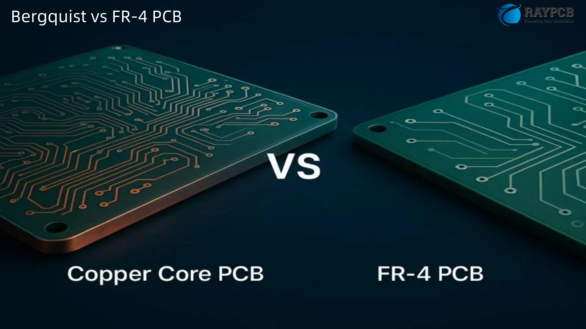
If you’ve narrowed your Bergquist dielectric shortlist down to the MP-06503 vs HT-04503, you’re already past the easy part of the selection process. Both are proven Thermal Clad Metal Core PCB (MCPCB) materials. Both use a 3-mil (76 ยตm) polymer/ceramic dielectric bonded to your choice of aluminum or copper base. Both carry UL recognition, are RoHS compliant, and support lead-free soldering. On paper, they look like minor variants of the same concept.

In practice, they are not. The differences between MP-06503 and HT-04503 run deeper than most comparison tables suggest โ€” and choosing the wrong one has real consequences for junction temperature, solder process latitude, long-term reliability, and ultimately, unit cost. This article goes through everything you need to make that call, backed by the actual datasheet numbers from both products.

The Short Answer on MP-06503 vs HT-04503

Before going further: if you’re in a time crunch, here it is. The MP-06503 is a multi-purpose, cost-effective dielectric with solid thermal performance (2.4 W/m-K product thermal conductivity) and a Tg of just 90ยฐC. The HT-04503 is a high-temperature dielectric with nearly double the product thermal conductivity at 4.1 W/m-K and a Tg of 150ยฐC. HT-04503 costs more. If your design runs hot, cycles hard, or needs gold-wire bonding compatibility, HT-04503 earns that premium. If it doesn’t, MP-06503 is the economically disciplined choice.

Everything below explains why in enough detail to back up that decision in a design review.

Understanding the Naming Convention First

Before comparing specs, it’s worth decoding the part numbers because the suffix reveals a structural difference that matters. Both end in “03,” meaning both use a 3-mil (76 ยตm) dielectric thickness. The difference is in the prefix number: “045” for HT-04503 and “065” for MP-06503, which refers to the approximate total laminate stack thickness in mils. The MP-06503 standard configuration sits on a thicker total stack (~65 mil / ~1.65 mm), while HT-04503 is configured around a thinner stack (~45 mil / ~1.14 mm base). This means when you order standard configurations, you are not comparing identical base thicknesses โ€” a factor that slightly affects the thermal resistance calculation at the system level and matters when designing enclosures and mechanical mounts.

Full Specification Comparison: MP-06503 vs HT-04503

The table below pulls directly from the official Bergquist datasheets for both products. These are the numbers that should be driving your selection, not marketing summaries.

Thermal Properties

PropertyMP-06503HT-04503Test Method
Product Thermal Conductivity2.4 W/m-K4.1 W/m-KMET 5.4-01-40000
Dielectric Thermal Conductivity1.3 W/m-K2.2 W/m-KASTM D5470
Thermal Resistance0.58 ยฐCยทcmยฒ/W0.32 ยฐCยทcmยฒ/WASTM D5470
Thermal Impedance0.65 ยฐC/W0.45 ยฐC/WMET 5.4-01-40000
Glass Transition (Tg)90ยฐC150ยฐCASTM E1356
Max Operating Temp (UL)130ยฐC140ยฐCUL 746B
Max Soldering Temp300ยฐC / 60s325ยฐC / 60sUL 796

Electrical Properties

PropertyMP-06503HT-04503Test Method
Dielectric Constant67ASTM D150
Dissipation Factor @ 1 kHz0.0030.0033ASTM D150
Dissipation Factor @ 1 MHz0.0170.0148ASTM D150
Capacitance65 pF/cmยฒ85 pF/cmยฒASTM D150
Volume Resistivity1ร—10ยนโต ฮฉยทm1ร—10ยนโด ฮฉยทmASTM D257
Surface Resistivity1ร—10ยนโด ฮฉ/sq1ร—10ยนยณ ฮฉ/sqASTM D257
Breakdown Voltage8.5 kVAC8.5 kVACASTM D149

Mechanical Properties

PropertyMP-06503HT-04503Test Method
Dielectric Thickness76 ยตm (3 mil)76 ยตm (3 mil)Visual
ColorWhiteWhiteVisual
Peel Strength @ 25ยฐC1.6 N/mm1.1 N/mmASTM D2861
CTE XY/Z below Tg40 ยตm/mยฐC25 ยตm/mยฐCASTM D3386
CTE XY/Z above Tg110 ยตm/mยฐC95 ยตm/mยฐCASTM D3386
Storage Modulus @ 25ยฐC12 GPa16 GPaASTM D4065
Storage Modulus @ 150ยฐC0.3 GPa7 GPaASTM D4065

The storage modulus comparison at 150ยฐC is one of the starkest data points in this whole analysis. MP-06503 at 0.3 GPa versus HT-04503 at 7 GPa โ€” that’s more than 20x greater stiffness retention in the HT dielectric at elevated temperature. The mechanical and electrical properties of the thermal clad will change when operating above the glass transition: the storage modulus declines, the CTE increases, and the peel strength reduces. For MP-06503 with a Tg of just 90ยฐC, any board that sees 100ยฐC+ is potentially operating above Tg. That’s not a cliff edge โ€” it’s a gradual degradation โ€” but it’s real.

The Tg Gap Is the Critical Issue

The 60ยฐC difference in glass transition temperature between MP-06503 (90ยฐC) and HT-04503 (150ยฐC) is the single most consequential spec in this comparison. It’s also the most frequently overlooked one.

A Tg of 90ยฐC sounds safe until you think about what temperatures a typical power board actually sees. An LED driver doing 30W in a luminaire with restricted airflow. A motor drive controller with a MOSFET dissipating 5W in a compact enclosure. A solid state relay mounted on an aluminum heatsink at 40ยฐC ambient. Any of these can push board-level temperatures to 80โ€“95ยฐC in normal operation, which puts MP-06503 right at or slightly above its Tg. The dielectric doesn’t fail catastrophically at Tg โ€” but over thousands of thermal cycles, the consequences accumulate as increased CTE mismatch stress at solder joints, weakened dielectric-to-copper adhesion, and gradual electrical degradation.

For the same designs, HT-04503’s Tg of 150ยฐC means you maintain a 50โ€“70ยฐC margin above operating temperature. That’s the kind of margin that keeps warranty return rates low.

Thermal Performance: What the Numbers Mean in Practice

The thermal resistance difference between the two โ€” 0.58 ยฐCยทcmยฒ/W for MP-06503 versus 0.32 ยฐCยทcmยฒ/W for HT-04503 โ€” is not just an academic spec delta. It translates directly to component junction temperature.

For a component dissipating 5W with a device footprint of 2 cmยฒ:

CalculationMP-06503HT-04503
Thermal resistance of dielectric0.58 ยฐCยทcmยฒ/W0.32 ยฐCยทcmยฒ/W
Effective ฮ”T across dielectric (5W, 2cmยฒ)1.45ยฐC0.80ยฐC

That’s 0.65ยฐC of additional junction temperature for every 5W per 2 cmยฒ when using MP-06503. Scale to a 20W component with a smaller die footprint and that gap widens materially. In high-brightness LED arrays where binning and color maintenance over lifetime are tightly controlled, every degree of junction temperature reduces lumen output and accelerates Tj-dependent degradation. HT-04503 buys real luminaire life in this application.

Where MP-06503 Wins

Higher Peel Strength

MP-06503 delivers 1.6 N/mm peel strength versus HT-04503’s 1.1 N/mm โ€” a 45% advantage. Peel strength matters primarily at room temperature during assembly (handling, singulation, test) and in applications with significant mechanical stress or vibration. For designs going into automotive interiors, consumer portable devices, or any product that gets physically handled in the field, MP-06503’s adhesion advantage is genuinely useful.

Better Volume and Surface Resistivity

MP-06503’s volume resistivity of 1ร—10ยนโต ฮฉยทm outperforms HT-04503’s 1ร—10ยนโด ฮฉยทm by a full decade. In high-impedance circuits or leakage-sensitive applications, this can matter โ€” though for the vast majority of power electronics applications, both values are comfortably sufficient.

Cost Advantage

MP-06503 is priced lower than HT-04503 across distributors. The cost difference is meaningful at production volumes โ€” typically in the range of 15โ€“30% lower material cost at the raw laminate level, though exact pricing depends on quantity, copper weight, base thickness, and current market conditions. For consumer electronics programs at tens of thousands of units per year, this gap compounds into real budget savings.

Where HT-04503 Wins

HT-04503 outperforms MP-06503 in every thermal and thermal-mechanical metric that matters for demanding applications. It has better product thermal conductivity (4.1 vs 2.4 W/m-K), lower thermal resistance (0.32 vs 0.58 ยฐCยทcmยฒ/W), higher Tg (150ยฐC vs 90ยฐC), higher max operating temperature (140ยฐC vs 130ยฐC), higher solder temperature rating (325ยฐC vs 300ยฐC), lower CTE (25 vs 40 ยตm/mยฐC below Tg), and dramatically better storage modulus retention at elevated temperatures (7 GPa vs 0.3 GPa at 150ยฐC).

The solder temperature rating is worth calling out specifically. HT-04503’s 325ยฐC/60s solder limit rating enables Eutectic Gold/Tin (AuSn) soldering and gold wire bonding โ€” processes that MP-06503’s 300ยฐC limit does not comfortably accommodate. For applications with bare die attachment, thermocompression bonding, or any process using higher-melting-point solders, HT-04503 is the only option between these two.

Application Fit Matrix

ApplicationMP-06503HT-04503Notes
Standard LED drivers (< 50W)โœ“โœ“MP-06503 is cost-effective here
High-power LED arrays (> 100W)โš โœ“Tg margin favours HT-04503
Consumer audio amplifiersโœ“โœ“MP-06503 adequate if Tj < 80ยฐC
Motor drives (compact, hot enclosures)โš โœ“Operating temp likely near MP Tg
Power conversion (industrial, > 150W)โš โœ“HT-04503 recommended
Solid state relaysโœ“โœ“Application-dependent
Automotive powertrain / EV invertersโœ—โœ“HT-04503 minimum; consider HT-07006
Bare die / wire bond attachmentโœ—โœ“Requires 325ยฐC solder capability
Cost-sensitive consumer productsโœ“โš MP-06503 better economics
Outdoor LED luminaires (hot climate)โš โœ“Ambient + self-heating risks MP Tg

โœ“ = well-suited | โš  = use with caution / thermal model required | โœ— = not recommended

The Cost vs Performance Decision Framework

Deciding between MP-06503 and HT-04503 really comes down to three questions:

1. What is your worst-case sustained board temperature? If the answer is consistently below 75ยฐC (giving a 15ยฐC margin to MP-06503’s Tg), MP-06503 is justified. If worst-case board temperature approaches or exceeds 80ยฐC, choose HT-04503.

2. What are your thermal cycling and lifespan requirements? Consumer products with 3โ€“5 year lifespans and moderate thermal cycling tolerate MP-06503 in appropriate temperature ranges. Automotive, industrial, and infrastructure products with 10โ€“20 year service life targets, or those cycling frequently through wide temperature swings, should default to HT-04503 for the Tg margin and lower CTE.

3. Does your assembly process require > 300ยฐC solder capability? Gold-tin solders, wire bonding, and some high-reliability attachment processes need the 325ยฐC rating that only HT-04503 provides. If this applies, the material decision is made for you.

For alternatives beyond the Bergquist Thermal Clad family, it’s worth knowing that Arlon PCB materials and other IMS laminate suppliers offer comparable product tiers. However, Bergquist’s extensive published qualification data and UL recognition often make it the lower-risk choice for products requiring safety agency certification.

Useful Resources and Datasheets

ResourceDescriptionLink
Bergquist HT-04503 Official DatasheetFull specs, thermal, electrical, mechanical propertiesDownload PDF
Bergquist MP-06503 Official Datasheet (Henkel TDS)Full specs including Tg, CTE, storage modulusDownload PDF
Bergquist MP-06503 Original DatasheetClassic format with dielectric comparison chartDownload PDF
Bergquist Thermal Clad Selection GuideComplete family comparison, design rules, assembly guidanceDownload PDF
Bergquist HT-07006 DatasheetNext-tier HT option for higher thermal demandsDownload PDF
Henkel / Bergquist Official Brand PageCurrent product catalog, regional distributor contactshenkel-adhesives.com
Digikey โ€“ Bergquist Thermal CladStocked parts, pricing, and availabilitydigikey.com
IPC-2221B Design StandardTrace width, clearance, dielectric design rulesipc.org

5 FAQs on MP-06503 vs HT-04503

1. Can I substitute MP-06503 for HT-04503 to reduce cost on an existing design?

Only if you’ve verified that your board temperature stays well below 75ยฐC under worst-case conditions (maximum ambient + maximum load + minimum airflow). The Tg difference โ€” 90ยฐC for MP-06503 versus 150ยฐC for HT-04503 โ€” means that designs originally tested with HT-04503 may have had thermal margins your thermal model never fully characterized. Run the full thermal analysis first. Also confirm your assembly process doesn’t use solder pastes or profiles that exceed 300ยฐC, since MP-06503’s solder limit is 300ยฐC vs HT-04503’s 325ยฐC.

2. Both products show the same 8.5 kVAC breakdown voltage โ€” does that mean they’re equivalent for high-voltage isolation?

Breakdown voltage is identical at 8.5 kVAC for both products at room temperature. However, dielectric breakdown performance degrades with temperature, and given MP-06503’s Tg of only 90ยฐC, the isolation performance at elevated board temperatures will degrade more than HT-04503. For applications where isolation integrity at high operating temperatures is critical โ€” industrial drives, UPS systems, EV on-board chargers โ€” HT-04503 maintains more consistent electrical isolation characteristics because it stays well below its Tg during normal operation.

3. Why does HT-04503 have lower peel strength than MP-06503?

Peel strength is a room-temperature mechanical property, and it reflects the adhesion of the polymer dielectric to the copper circuit layer. The HT dielectric uses a different polymer chemistry optimized for high-temperature performance โ€” specifically for superior storage modulus retention and low CTE at elevated temperatures. That chemistry trades off some room-temperature peel strength. At 1.1 N/mm, HT-04503 is still well within acceptable adhesion limits for standard SMT assembly and handling. The practical risk is marginal for the applications HT-04503 targets; those products aren’t getting physically abused at room temperature.

4. What’s the next step up from HT-04503 if it’s still not enough?

The Bergquist HT-07006 uses the same HT chemistry on a thicker (6 mil / ~150 ยตm) dielectric, which improves thermal resistance slightly while increasing voltage isolation capability. For truly extreme thermal demands, the CML (Ceramic-Metal Laminate) dielectric offers the highest thermal conductivity in the Bergquist range and is designed for direct replacement of ceramic substrates. If your application requires it, CML supports bare die mounting and thermocompression bonding at temperatures beyond what even HT-04503 can handle.

5. Is the dielectric thickness the same for both products, and does that affect which one I should choose?

Yes, both MP-06503 and HT-04503 use a 3-mil (76 ยตm) dielectric layer. Since the dielectric thickness is identical, the thermal resistance difference is entirely attributable to the higher thermal conductivity of the HT dielectric polymer/ceramic blend. The 3-mil dielectric in both products provides a breakdown voltage of 8.5 kVAC. For applications above 480 VAC, Bergquist’s design guidelines recommend specifying a dielectric thickness greater than 3 mil regardless of which family you choose.

Conclusion

When it comes to MP-06503 vs HT-04503, the comparison isn’t really about marginal performance differences โ€” it’s about two different classes of application. MP-06503 is a capable, cost-competitive dielectric for moderate-temperature, moderate-power designs where budget matters and thermal conditions are well-controlled. HT-04503 is the choice for designs where board temperatures push toward 100ยฐC+, where thermal cycling is aggressive, where long service life is expected, or where higher-temperature solder processes are required.

Use MP-06503 when you’ve verified the thermal and process margins. Use HT-04503 when any of those margins are tight, when the application demands it, or when the cost of a field failure exceeds the cost of the material upgrade many times over. In the context of a full product BOM, the price difference between the two is rarely significant โ€” but the reliability difference can be.

All specifications referenced are from official Bergquist/Henkel datasheets. Verify against current documentation before design lock-in, as material formulations are subject to revision.

Suggested Meta Description

Meta Description (157 characters):

Bergquist MP-06503 vs HT-04503: full spec comparison of thermal conductivity, Tg, peel strength & cost. Engineer’s guide to choosing the right MCPCB dielectric.

Metal Core PCB Manufacturing Process: A Complete Step-by-Step Guide

Three meta description optionsย are at the end of the file โ€” Option B (155 chars) is the tightest fit for Google’s SERP display limit; Option A works well if your CMS allows a longer meta.

If you’ve ever held a high-power LED streetlight, opened a car headlight module, or looked at a power inverter board, there’s a good chance you were handling a metal core PCB (MCPCB). These boards don’t look radically different from standard FR4 boards at first glance โ€” same copper traces, same solder mask โ€” but their internal structure is fundamentally different, and so is the way they’re made.

This guide walks through the metal core PCB manufacturing process from raw material selection through final electrical test, with enough detail to help engineers, buyers, and design teams understand what actually happens on the factory floor โ€” and why certain design decisions matter so much.

What Is a Metal Core PCB and Why Does It Exist?

A metal core PCB (also called MCPCB, IMS PCB, thermal clad, or insulated metal substrate PCB) replaces the conventional FR4 fiberglass core with a thermally conductive metal base โ€” most commonly aluminum, though copper and steel alloys are also used. The purpose is simple: heat removal.

Standard FR4 has a thermal conductivity of roughly 0.25โ€“0.30 W/mยทK. Aluminum sits around 200 W/mยทK, and copper pushes 390โ€“400 W/mยทK. That gap โ€” three orders of magnitude โ€” is why high-power LEDs, automotive modules, motor drives, and RF power amplifiers are almost universally built on metal core substrates.

The board structure is a three-layer sandwich:

LayerMaterialTypical ThicknessFunction
Copper Circuit LayerElectrolytic copper foil1 oz to 6 oz (35โ€“210 ฮผm)Current-carrying traces and pads
Dielectric LayerThermally conductive polymer50โ€“150 ฮผmElectrical insulation + thermal path
Metal SubstrateAluminum / Copper / Steel1.0โ€“3.2 mmStructural support + heat spreader

The dielectric layer is the most performance-critical element. It must electrically isolate the copper from the grounded metal core while allowing heat to flow freely downward. Modern dielectric materials achieve 1 to 8 W/mยทK, far above the 0.3 W/mยทK typical of standard PCB prepreg.

Metal Core PCB Layer Structure and Stack-Up Options

Before diving into manufacturing, it helps to understand the stack-up types your fabricator may offer. The process steps vary slightly depending on which structure you’ve designed.

Single-Layer MCPCB

The simplest configuration: one copper circuit layer on top of the dielectric and metal base. Surface-mount components only. This covers the vast majority of LED lighting boards, LED driver modules, and simple power supplies.

Double-Sided MCPCB

Two copper layers on opposite sides of the metal core. PTH (plated through-holes) are possible but require careful design โ€” the drill must be oversized by 40โ€“50 mils around the metal core to prevent a short circuit between the lead and the aluminum base.

Two-Layer MCPCB (Same-Side Stack)

Both copper circuit layers are on the same side of the metal core, with the metal base at the bottom. This allows more routing complexity while maintaining single-sided assembly.

Multilayer MCPCB

Three or more circuit layers with thermally conductive prepreg between them, bonded to the metal substrate. Significantly more expensive to fabricate due to lamination complexity. Used in industrial power modules, automotive ECUs, and aerospace applications.

COB MCPCB (Chip-on-Board)

The die is bonded directly to the metal core surface โ€” no dielectric layer under the chip. Thermal conductivity of the path under the chip approaches that of the base metal itself (>200 W/mยทK for aluminum). Used in ultra-high-power LED engines and automotive solid-state lighting.

Metal Core PCB Manufacturing Process: Step-by-Step

Step 1: Design Review and DFM Check

Manufacturing starts long before copper hits a laminator. The engineer’s Gerber files (or ODB++) are run through a Design for Manufacturability (DFM) check. For MCPCB, this is more critical than for FR4 because several failure modes are unique to metal core boards:

  • PTH placement too close to the metal core edge
  • Trace clearance violations near metal-core cutouts
  • Dielectric layer thickness inconsistency causing hi-pot failures
  • Insufficient copper-to-edge clearance on routed panels

Tooling holes, panel size, V-score layout, and copper weight are all verified before the process begins. Most fabricators use dedicated CAM software with MCPCB-specific rule sets.

Step 2: Base Material Preparation and Panel Cutting

The metal base sheet arrives at the factory as large-format stock. Common alloys include:

MetalCommon AlloyThermal ConductivityNotes
Aluminum5052 H32~138 W/mยทKMost popular; good balance of strength and cost
Aluminum6061 T6~167 W/mยทKBetter machinability; used when CNC work is heavy
CopperC1100~391 W/mยทKPremium thermal performance; heavier and more expensive
Steel (Iron)Cold-rolled~50 W/mยทKHarder; used where structural rigidity matters more than thermal

Aluminum 5052 H32 dominates the LED lighting market โ€” it’s the practical sweet spot of thermal performance, weight, machinability, and price. The stock sheets are sheared or CNC-cut to the panel dimensions specified in the tooling drawing. Edge burrs are deburred before further processing.

Step 3: Drilling

Drilling happens before lamination on most aluminum MCPCB lines. Aluminum is soft enough that standard carbide drill bits cut cleanly, but tooling parameters differ from FR4:

  • Feed ratesย are typically higher than FR4
  • Drill bit geometryย is optimized for non-abrasive metal โ€” different rake angle than ceramic-filled laminates
  • Hole registrationย must be tighter because the metal core won’t compress to accept tolerance creep the way FR4 does

For PTH boards, each hole destined for a plated via or component lead must have the metal core pre-drilled 40โ€“50 mils oversize. This clearance zone is later filled with resin to prevent shorts. For NPTH (non-plated) mounting holes, standard sizing applies.

CNC drilling machines run at high RPM with automated bit selection. Each hole is drilled individually, which makes the process time-intensive on complex multilayer panels.

Step 4: Surface Pre-Treatment of the Metal Core

Before the dielectric is laminated, the aluminum surface must be chemically cleaned and roughened to ensure adhesion. This typically involves:

  1. Alkaline degreasingย โ€” removes oils, fingerprints, and machining residues
  2. Micro-etchingย โ€” chemically roughens the surface to improve dielectric bonding
  3. Rinse and dryย โ€” thorough rinsing prevents contamination carry-over

Copper core boards may receive an additional oxide treatment to enhance adhesion. This step is invisible in the final product but has an enormous impact on long-term delamination resistance and thermal cycling durability.

Step 5: Dielectric Lamination

This is the step that defines MCPCB thermal performance. The thermally conductive dielectric โ€” typically supplied as a prepreg sheet or as a pre-applied film on the copper-clad laminate โ€” is bonded to the metal base under controlled heat and pressure.

Common dielectric materials in use:

Material TypeThermal ConductivityVoltage BreakdownNotes
Standard epoxy-filled1.0โ€“1.5 W/mยทKโ‰ฅ3,000 VCost-effective for most LED applications
Ceramic-filled polymer2.0โ€“3.0 W/mยทKโ‰ฅ3,000 VMid-tier; good balance for automotive
High-performance ceramic4.0โ€“8.0 W/mยทKโ‰ฅ5,000 VPower modules, high-density LED arrays
Polyimide-based1.0โ€“2.0 W/mยทKโ‰ฅ4,000 VHigh-temperature stability, flexible options

Popular material brands you’ll see in specifications include Bergquist (now Henkel), Ventec, Iteq, and Arlon. For specialty applications like Arlon PCB where extreme temperature cycling is expected, material selection becomes a critical engineering decision, not just a cost consideration.

Lamination is carried out in a hot press at typically 170โ€“200ยฐC and 15โ€“30 kgf/cmยฒ. Cure time and temperature profile determine the degree of cross-linking in the dielectric, which affects long-term thermal stability.

Step 6: Copper Foil Application and Imaging

If the dielectric and copper foil haven’t arrived as a pre-laminated composite, the copper foil is pressed onto the dielectric simultaneously with lamination. The resulting copper-clad metal substrate (CCMS) is then ready for circuit imaging.

The imaging process transfers the circuit pattern from the Gerber data onto the copper surface:

  1. Surface cleaning and micro-etchย of the copper foil
  2. Dry film photoresist laminationย โ€” a UV-sensitive film is hot-rolled onto the copper
  3. UV exposureย through a phototool (or direct laser imaging on modern lines) โ€” the resist hardens where copper will remain
  4. Developmentย โ€” unexposed resist washes away in sodium carbonate solution, exposing bare copper in etch areas

Step 7: Etching

The exposed copper (areas that will become gaps between traces) is removed in an alkaline cupric chloride or ammonium persulfate etch line. The etching process is tightly controlled:

  • Etch factor (undercut): Managed by etchant concentration, temperature (50โ€“55ยฐC typically), and conveyor speed
  • Uniformity: Critical on metal core panels because the board doesn’t flex โ€” any warping would cause non-uniform etch rates
  • Over-etching: Reduces trace width and increases resistance; particularly damaging on fine-pitch designs
  • Under-etching: Leaves copper slivers that cause short circuits or hi-pot failures

After etching, the resist is stripped in a sodium hydroxide solution. The panel enters AOI (Automated Optical Inspection) at this point โ€” cameras compare the actual copper pattern against the Gerber reference to flag opens, shorts, and trace anomalies.

Step 8: Solder Mask Application

The solder mask protects the copper traces from oxidation, prevents solder bridging during assembly, and โ€” for LED boards โ€” often improves optical performance. Application methods include:

Liquid Photo-Imageable (LPI) Solder Mask: Screened or curtain-coated, then UV-exposed and developed. Provides tight dimensional control of pad openings and good adhesion to the copper and dielectric. This is the dominant process for MCPCB.

Ink Jet: Used for prototype quantities and complex, tightly-registered mask openings.

Solder mask colors for MCPCB:

ColorTypical Use Case
WhiteLED lighting boards โ€” increases light reflectivity (>85%)
BlackAutomotive, industrial โ€” reduces light reflection, hides traces
GreenGeneral-purpose, cost-optimized
Blue / RedBranding, differentiation

For LED applications, white solder mask with high light reflectance is the standard specification. After application, the mask is fully cured in a convection oven at 150ยฐC.

Step 9: Silkscreen (Legend Printing)

Component reference designators, polarity marks, logo, and revision information are printed in epoxy ink using screen printing or inkjet. Standard colors are white on green/black mask and black on white mask. The silkscreen aids PCB assembly and service technicians in identifying components.

Step 10: Surface Finish

The exposed copper pads (where components will be soldered) receive a surface finish to protect against oxidation and ensure good solderability. For MCPCB, the most common finishes are:

FinishProcessShelf LifeBest For
HASL (Lead-Free)Hot Air Solder Level12 monthsGeneral power electronics
ENIGElectroless Nickel Immersion Gold12 monthsFine-pitch SMT, wire bonding
Immersion SilverChemical silver deposit6โ€“12 monthsGood planarity, cost-effective
OSPOrganic Solderability Preservative6 monthsSingle reflow, cost-sensitive
Immersion TinChemical tin deposit6 monthsPress-fit connectors

For LED arrays requiring wire bonding (COB process), ENIG is essentially mandatory. The gold layer provides the bond-wire landing surface.

Step 11: Routing, V-Scoring, and Panel Separation

The final board outline is cut using one of three methods:

CNC Routing: A carbide end mill traces the board perimeter and any internal slots or cutouts. Generates individual boards or arrays with tabs. Routing aluminum produces fine metallic chips โ€” proper chip evacuation and filtration are essential to prevent contamination.

V-Scoring: A V-groove is scored to approximately 1/3 board thickness on both sides. Boards snap apart during assembly or at the customer’s facility. Efficient for rectangular panels with straight-edge boards.

Punching: Used for high-volume, simple-outline MCPCB boards (many LED star boards, for instance) where die tooling cost is justified by volume.

One consideration unique to aluminum MCPCB: burr formation. Aluminum is ductile and tends to leave a raised burr on cut edges. Quality fabricators perform a deburring step, and the edge quality should be verified in incoming inspection.

Step 12: Electrical Testing

Every MCPCB that ships should pass two categories of electrical test:

Continuity / Hi-Pot (Isolation) Testing: A flying-probe tester or bed-of-nails fixture applies 500V to 3,000V AC between the copper circuit and the metal base. Any breakdown in the dielectric โ€” from a pinhole, inclusion, or lamination void โ€” will cause a failure. This is non-negotiable. A failed hi-pot test on a field-installed board can mean a serious safety hazard, especially in mains-connected LED drivers.

Continuity and Short Circuit Testing: The circuit is verified for opens and shorts according to the netlist.

Most manufacturers also test:

  • Thermal resistanceย on sample boards (per IEC 62758 or equivalent)
  • Peel strengthย of the dielectric-to-metal bond
  • Bow and twistย โ€” the metal core should keep these values low, but warped panels still occur

Step 13: Final Inspection and Quality Control

Visual inspection (human and AOI) checks for:

  • Solder mask coverage uniformity and adhesion
  • Surface finish appearance and coverage
  • Routing edge quality
  • Silkscreen registration
  • Cosmetic defects

Dimensional inspection verifies board outline, hole locations, and thickness. Thermal conductivity is verified by quality sampling using laser flash analysis or transient hot-wire methods on representative coupons.

Step 14: Packaging and Shipment

MCPCB packaging deserves more attention than engineers sometimes give it. Aluminum oxidizes. Humidity causes condensation under vacuum-sealed bags if temperature differentials are large. Most manufacturers:

  • Interleave boards with foam or corrugated slip sheets to prevent surface-to-surface abrasion
  • Vacuum seal in moisture barrier bags with desiccant
  • Mark bags with board ID, quantity, date code, and thermal/electrical spec

Key Material Specifications Quick Reference

Aluminum Grades Comparison

PropertyAl 5052 H32Al 6061 T6Cu C1100
Thermal Conductivity~138 W/mยทK~167 W/mยทK~391 W/mยทK
Tensile Strength228 MPa310 MPa220 MPa
Density2.68 g/cmยณ2.70 g/cmยณ8.94 g/cmยณ
MachinabilityGoodExcellentModerate
Cost IndexLowLowโ€“MediumHigh

Typical MCPCB Standard Specifications

ParameterStandard ValueHigh-Performance
Dielectric thermal conductivity1.0 W/mยทK3.0โ€“8.0 W/mยทK
Dielectric thickness100โ€“130 ฮผm50โ€“75 ฮผm
Dielectric breakdown voltageโ‰ฅ3,000 Vโ‰ฅ5,000 V
Copper weight1 oz (35 ฮผm)2โ€“3 oz (70โ€“105 ฮผm)
Metal base thickness1.0โ€“1.6 mm2.0โ€“3.2 mm
Minimum trace/space5/5 mil3/3 mil (advanced)
Board thermal resistance (ฮธboard)0.5โ€“1.5 ยฐC/W0.1โ€“0.4 ยฐC/W

MCPCB vs FR4: Performance Comparison

ParameterFR4Standard MCPCB (Al)High-Performance MCPCB (Cu)
Substrate thermal conductivity0.25โ€“0.30 W/mยทK~138 W/mยทK~391 W/mยทK
Dielectric thermal conductivity0.30 W/mยทK1.0โ€“3.0 W/mยทK2.0โ€“8.0 W/mยทK
Typical junction-to-board ฮธVery highModerateLow
Mechanical rigidityModerateHighVery High
Weight (1.6mm board)~330 g/mยฒ~450 g/mยฒ~1,600 g/mยฒ
Relative costLowMediumHigh
Operating temperatureUp to 130ยฐC (Tg)Up to 150โ€“180ยฐCUp to 200ยฐC+

Critical MCPCB Design Rules for Manufacturability

Engineers who haven’t worked extensively with metal core boards regularly hit the same snags. Here are the design rules that matter most:

SMT preferred over PTH: The metal core creates a direct short risk for any lead that passes through the board. If you must use PTH components, clear the metal core by 40โ€“50 mils around each hole and fill the annular ring with dielectric resin in your fabrication notes.

Edge clearance for traces: Maintain at least 0.5mm (20 mil) copper-to-board-edge clearance. Routing aluminum can cause micro-burrs that creep toward exposed traces.

Thermal pad exposure: For bottom-cooled packages (DPAK, DยฒPAK, TO-263), make sure your thermal pad solder paste coverage and stencil aperture are specified correctly. Solder voids under the pad translate directly to increased thermal resistance.

Via-in-pad on MCPCB: Standard via-in-pad with resin fill is feasible but must be specified explicitly. Unfilled vias under SMT pads will cause voiding in the solder joint.

Dielectric thickness selection: Thinner dielectric = lower thermal resistance but higher risk of hi-pot failure and pinhole defects. For mains-isolated LED drivers, don’t push below 100 ฮผm without validating with your fabricator. For Class III or SELV-only boards, thinner dielectrics (75 ฮผm) are more common.

Solder mask over bare metal edges: Specify whether the metal core edge should be masked or left bare. Bare aluminum edges oxidize โ€” not a functional concern for most applications, but worth noting in cosmetic-sensitive products.

Common MCPCB Manufacturing Defects and Root Causes

DefectRoot CausePrevention
Dielectric delaminationPoor surface prep, moisture in laminateStrict pre-treatment, controlled humidity storage
Hi-pot failureDielectric pinhole or inclusionMaterial quality control, post-etch inspection
Trace undercutOver-etching, etchant imbalanceClosed-loop etch control, frequent bath monitoring
Warped panelAsymmetric copper distribution, improper lamination pressureBalance copper pour on both sides, validated press profile
Poor solder mask adhesionSurface contamination, wrong mask viscosityThorough plasma clean before mask application
Burrs on routed edgesDull routing bit, wrong feed rateTool change schedule, deburring step
Solder wicking to metal core (PTH)Insufficient resin plug in PTHOversized core clearance, confirmed plug fill before solder

Frequently Asked Questions About Metal Core PCB Manufacturing

Q1: How long does it take to manufacture a metal core PCB?

Standard lead times for aluminum single-layer MCPCB run 5โ€“10 working days for prototype quantities. Expedited services (48โ€“72 hours) are available from some manufacturers for common stack-ups and standard materials. Multilayer MCPCB or copper-core boards typically need 10โ€“15 working days due to additional lamination and inspection steps.

Q2: Can I use a standard FR4 PCB assembly line for MCPCB assembly?

Mostly yes, with some adjustments. The reflow profile may need tuning since the aluminum core acts as a heat sink and causes slower ramp-up. Pick-and-place machines handle MCPCB panels normally. The main issue is handling โ€” aluminum boards are heavier and have sharper edges than FR4. Wave soldering is generally avoided because the large metal mass makes uniform preheat difficult.

Q3: What is the difference between an IMS PCB and an MCPCB?

They are the same thing. IMS (Insulated Metal Substrate) and MCPCB (Metal Core PCB) describe an identical structure โ€” a copper circuit layer, a thermally conductive dielectric insulator, and a metal base. Other names you’ll encounter: thermal clad PCB, metal-clad PCB, aluminum-clad PCB, and thermally conductive PCB.

Q4: What dielectric thermal conductivity should I specify for an LED lighting application?

For general LED retrofit lamps and decorative lighting, 1.0โ€“1.5 W/mยทK is adequate. For high-power street lighting, grow lights, or stadium lighting where junction temperature control is critical, specify 2.0โ€“3.0 W/mยทK. Automotive LED headlights often run with 3.0+ W/mยทK dielectrics. Only push to 6โ€“8 W/mยทK for extreme-density applications โ€” cost jumps significantly.

Q5: Can MCPCB be made with multiple copper weights on the same board?

Technically yes โ€” stepped copper is achievable through selective electroplating (plating-up specific areas) or by using heavy copper foil and etching away. In practice, most manufacturers offer 1 oz, 2 oz, or 3 oz as a uniform copper weight across the board. Mixed-weight designs increase cost and should only be specified when there’s a genuine current-handling justification.

Useful Resources for MCPCB Engineers

ResourcePurposeLink
IPC-4101Specification for base materials for rigid and multilayer PCBs, including metal-core constructionsipc.org
IEC 62758Test methods for MCPCB thermal resistanceiec.ch
Ventec VT-4A1 DatasheetWidely used 1.0 W/mยทK MCPCB dielectric datasheetventec-group.com
Bergquist / Henkel IMS Product SelectorThermal material selection tool covering HPL, MP, and GP serieshenkel-adhesives.com
RayPCB MCPCB CapabilitiesFabricator capability spec sheet for aluminum and copper MCPCBraypcb.com
Semiconductor JEDEC JESD51Thermal measurement standards for components on PCBsjedec.org

Summary: What Makes MCPCB Manufacturing Different

The metal core PCB manufacturing process follows the same conceptual sequence as standard FR4 fabrication โ€” design, image, etch, drill, mask, finish, test โ€” but every step is executed against a different set of constraints. The metal base demands pre-treatment for adhesion. Drilling requires controlled chip management. Lamination parameters are material-specific and performance-critical. Etching must be uniform across a rigid, non-compliant substrate. And electrical testing must include hi-pot validation that FR4 lines may not routinely perform.

For engineers specifying MCPCBs, the most important decisions happen before a Gerber file ever reaches a fabricator: choosing the right base metal, selecting the correct dielectric thermal conductivity for your heat budget, and designing pad geometries and PTH clearances that respect the unique constraints of metal-core construction.

For manufacturers, MCPCB is not a “just run it through the FR4 line” product. It requires dedicated equipment, validated process parameters for each material combination, and a quality system that takes hi-pot testing as seriously as visual inspection.

Meta Description Suggestion:

Option A (58 words): Learn the complete metal core PCB manufacturing process step by step โ€” from aluminum substrate preparation and dielectric lamination to etching, solder mask, surface finish, and electrical testing. Includes material comparison tables, design rules for MCPCB, common defects and their causes, and 5 engineer FAQs. Written from a PCB engineer’s perspective for designers, buyers, and manufacturing engineers.

Option B (155 characters โ€” tight fit for Google SERP): Step-by-step guide to metal core PCB manufacturing: material selection, drilling, lamination, etching, surface finish, hi-pot testing, and design rules for MCPCB engineers.

Option C (155 characters โ€” keyword-focused): Complete metal core PCB manufacturing process guide covering aluminum vs copper substrates, dielectric selection, etching, solder mask, testing, and MCPCB design rules.

Metal Core PCB for Automotive Electronics: Bergquist Dielectric Selection

Metal core PCB for automotive electronics: how to select Bergquist HT, MP & CML dielectrics for LED headlights, EV inverters, ADAS & underhood applications.

Automotive electronics have become one of the most demanding environments a PCB designer will ever face. Unlike a consumer product that might see a few years of indoor use at mild temperatures, a board inside a vehicle could be subjected to engine-bay heat spikes above 125ยฐC, -40ยฐC cold soaks in a Norwegian winter, 10โ€“15 years of continuous thermal cycling, vibration from road surfaces, and EMI from high-voltage bus bars running centimetres away. Against that backdrop, metal core PCB automotive applications represent one of the clearest use cases where moving off FR-4 isn’t optional โ€” it’s the only path to the reliability targets the industry demands.

This guide focuses on how to select the right Bergquist Thermal Clad dielectric for automotive applications. It covers what the automotive environment actually demands, how Bergquist’s dielectric families map to different vehicle subsystems, the specific specs that drive the decision, and design rules that affect reliability in the field. Whether you’re working on EV inverters, headlight driver modules, or ADAS power supply boards, the selection principles are the same โ€” the numbers just move around.

Why Standard FR-4 Falls Short in Automotive Metal Core PCB Design

The fundamental issue is thermal conductivity. Standard FR-4 laminate delivers approximately 0.2โ€“0.3 W/m-K. That figure is adequate when power dissipation is low and the board can breathe freely. In automotive electronics, neither condition reliably holds. Metal-core PCBs, where the metal core is an aluminum alloy base layer, are particularly suitable for heat transfer applications, and standard FR-4 may not suffice for high-temperature applications where high-Tg materials are preferred for improved thermal stability.

The problem compounds when you factor in lifecycle requirements. Unlike consumer electronics with typical lifespans of 2โ€“3 years, automotive electronics must maintain reliability for 15 years or more under conditions that include extreme temperature cycling, humidity, vibration, and electrical noise. Every degree of margin you don’t have at the thermal design stage erodes reliability over that service window.

Metal core PCB for automotive applications solves this by replacing the FR-4 core with a metal base โ€” typically aluminum โ€” and bonding a proprietary polymer/ceramic dielectric between that base and the copper circuit layer. The dielectric transfers heat efficiently while maintaining electrical isolation. The metal base then spreads and conducts that heat to a chassis mount, enclosure wall, or dedicated heatsink. The result is a board that manages its own thermal load without passive heatsinks bolted to individual components.

The Automotive Thermal Environment: Zones and Temperature Requirements

Before selecting a Bergquist dielectric, you need to anchor the selection to the actual temperature environment your board will live in. Automotive electronics engineers typically work with defined temperature zones that drive material selection choices.

Automotive Temperature Zones and Typical Requirements

ZoneLocationTypical Operating TempThermal Cycling RangeNotes
Under-hood (powertrain adjacent)Engine bay, near exhaust85ยฐC to 125ยฐC ambient-40ยฐC to +150ยฐCMost demanding; IGBT modules, motor controllers
Under-hood (body electronics)Engine bay, moderate zone70ยฐC to 105ยฐC ambient-40ยฐC to +125ยฐCFuel systems, lighting controllers
Passenger cabinInterior electronics40ยฐC to 85ยฐC ambient-40ยฐC to +85ยฐCInfotainment, HVAC control, seat systems
Exterior bodyLighting, sensors40ยฐC to 95ยฐC ambient-40ยฐC to +105ยฐCLED headlights, tail lights, radar
EV powertrainInverter, BMS60ยฐC to 105ยฐC ambient-40ยฐC to +150ยฐCHigh current, high voltage, EMI intensive

Automotive-grade components must withstand extreme temperatures (-40ยฐC to 150ยฐC) and demonstrate exceptional reliability over 15-year lifespans, complying with rigorous quality standards such as AEC-Q100 and ISO 26262. The dielectric you choose needs to maintain its mechanical and electrical properties across that entire range, not just at the design point.

Bergquist Thermal Clad for Automotive: The Dielectric Families That Matter

Bergquist’s Thermal Clad Insulated Metal Substrate platform is a three-layer construction โ€” copper circuit layer, polymer/ceramic dielectric, and metal base โ€” with several dielectric families available. In automotive applications, the relevant options are the HT (High Temperature) and CML families, with the MP series applicable in lower-stress automotive zones. Here’s how they map to automotive work.

HT-04503 and HT-07006: The Automotive Workhorses

The HT dielectric family is the primary choice for metal core PCB automotive applications wherever temperatures are elevated. The HT-04503 delivers a product thermal conductivity of 4.1 W/m-K, a thermal resistance of 0.32ยฐCยทcmยฒ/W, a Tg of 150ยฐC, and a UL-rated maximum operating temperature of 140ยฐC. The max soldering temperature of 325ยฐC/60s enables Eutectic Gold/Tin solder and gold wire bonding โ€” both relevant for automotive bare-die applications.

HT dielectrics are UL solder rated at 325ยฐC/60 seconds, enabling Eutectic Gold/Tin solders, and ENEPIG (Electroless Nickel/Electroless Palladium/Immersion Gold) is recommended for gold wire applications.

The HT-07006 steps up to a 6-mil (152 ยตm) dielectric on the same HT polymer chemistry, which improves voltage isolation for higher-bus-voltage applications โ€” directly relevant to 400V and 800V EV architectures.

MP-06503: Cabin and Lower-Stress Automotive Zones

The MP-06503 with 2.4 W/m-K thermal conductivity and a Tg of 90ยฐC is suitable only for automotive zones where board temperatures stay well below 80ยฐC. In practice, that means cabin electronics, infotainment power supply boards, HVAC control modules, and ambient lighting drivers where thermal cycling is moderate. For underhood or EV powertrain applications, MP-06503’s 90ยฐC Tg creates unacceptable margin risk. Applying it in a zone that routinely pushes 100ยฐC board temperature is a reliability time bomb.

CML: High-Reliability Automotive and Ceramic Replacement

The Ceramic-Metal Laminate (CML) dielectric is Bergquist’s highest-performance option and is used in automotive applications requiring direct replacement of ceramic substrates โ€” typically power modules in EV inverters, motor drives, and high-frequency switching circuits. CML uses a glass carrier (unique in the Bergquist range) and supports bare-die mounting and thermocompression bonding at temperatures beyond what even HT can handle.

Bergquist Dielectric Selection Summary for Automotive Applications

DielectricThermal ConductivityTgMax Op. TempBest Automotive Use Case
MP-065032.4 W/m-K90ยฐC130ยฐCCabin electronics, body control, low-stress ancillaries
HT-045034.1 W/m-K150ยฐC140ยฐCLED headlights, motor drives, EV BMS, solid state relays
HT-070064.1 W/m-K150ยฐC140ยฐCEV inverters, high-voltage isolation (6-mil dielectric)
CMLHighest in rangeHighHighestBare-die power modules, ceramic substrate replacement

Key Automotive-Specific Design Requirements for Metal Core PCB

Thermal Cycling and CTE Matching

In automotive metal core PCB design, coefficient of thermal expansion (CTE) mismatch is a primary cause of field failures. The Bergquist HT-04503 has a CTE of 25 ยตm/mยฐC below Tg, which is substantially lower than MP-06503’s 40 ยตm/mยฐC below Tg. Lower CTE is directly beneficial in automotive because it means less dimensional movement per thermal cycle, which reduces solder joint fatigue at component interfaces.

Metal core PCBs help satisfy operational requirements as they provide greater structural integrity and thermal conductivity than boards built on FR-4 laminates. The higher thermal conductivity of these boards helps ensure temperature distribution is uniform during thermal cycling, which prevents hot spots from forming near active components.

When the base material is aluminum, CTE mismatch between the board and ceramic-packaged devices is a real issue. For power semiconductor packages with ceramic bodies โ€” common in automotive power electronics โ€” copper-base Thermal Clad can provide better CTE compatibility than aluminum. For mechanical strength demand scenarios such as automotive electronics and industrial control, copper substrates with CTE close to silicon chips or aluminum substrates for lightweight applications should be selected based on priority.

Aluminum vs. Copper Base for Automotive Metal Core PCB

The base metal choice is almost as important as the dielectric choice in automotive MCPCB design.

ParameterAluminum BaseCopper Base
Thermal Conductivity~205 W/m-K~390 W/m-K
Density~2.7 g/cmยณ~8.9 g/cmยณ
CTE~23 ยตm/mยฐC~17 ยตm/mยฐC
MachinabilityExcellentMore difficult
Relative CostLowerHigher (significantly)
Best Automotive UseLED lighting, cabin electronics, general body electronicsEV inverter modules, high-reliability power devices, bare-die mounting

Aluminum base is the right choice for the majority of automotive applications โ€” it is lighter, easier to machine, and cost-effective. Copper base is specified when the application places power semiconductor packages with ceramic bodies directly on the substrate and CTE mismatch fatigue over 500+ thermal cycles would otherwise compromise solder joint reliability. Thermal interface materials are expected to be robust with respect to environmental and ambient conditions, reduce thermal stress between two regions with very different coefficients of thermal expansion, and have a long working life without leakage.

Voltage Isolation in 48V and High-Voltage EV Architectures

The automotive industry’s shift to 48V mild hybrid systems and 400V/800V EV architectures has fundamentally changed the voltage isolation requirements for metal core PCB in automotive designs. A standard 3-mil (76 ยตm) Thermal Clad dielectric provides breakdown voltage of 8.5 kVAC โ€” adequate for many 48V and even 400V applications with appropriate creepage and clearance margins. For 800V systems and traction inverter boards where bus voltage spikes can be significant, the HT-07006’s 6-mil (152 ยตm) dielectric provides greater isolation headroom.

For a 400V system in a polluted automotive environment with standard material, minimum creepage distances must be carefully calculated. Use MCPCB if thermal simulation predicts component temperatures above 140ยฐC with FR-4 solutions, or if space constraints prevent sufficient thermal vias.

AEC-Q and IATF 16949 Compliance Considerations

Automotive qualification doesn’t stop at the component level โ€” substrate materials are part of the supplier qualification chain. Bergquist’s Thermal Clad materials undergo rigorous internal qualification including mechanical property validation, adhesion testing, temperature cycling (-40ยฐC to 150ยฐC, 500 cycles), thermal and electrical stress to 2000 hours, and 85ยฐC/85%RH/100V humidity-bias testing. The lab facilities at Bergquist are UL certified and manufacturing facilities are ISO 9001 certified. For Tier 1 automotive supply chains operating under IATF 16949, this documentation trail is not optional โ€” it’s part of the PPAP package.

Automotive PCBs must pass stringent tests such as thermal cycling, thermal shock, and temperature humidity before being installed on the vehicle. Full traceability of materials, components, and manufacturing processes is mandatory for recalls and warranty claims.

Automotive Application Deep Dive: Where Metal Core PCB Excels

LED Automotive Headlights and Tail Lights

LED automotive lighting is one of the most thermally demanding MCPCB applications in production vehicles. High-beam LED modules can dissipate 30โ€“50W in a compact housing with restricted airflow. Junction temperature management is critical because LED lumen output, color temperature, and operational life all degrade with rising Tj. The Bergquist HT-04503 at 4.1 W/m-K with a Tg of 150ยฐC is the standard choice for automotive headlight LED modules. For extremely high-lumen designs, the HPL-03015 (Tg 185ยฐC, 3.0 W/m-K on a 38 ยตm dielectric) achieves very low thermal resistance. Bergquist Thermal Clad materials are widely specified for automotive electronics including LED lighting, electric vehicles, power conversion, and motor drivers.

EV Inverter and Motor Drive Boards

EV traction inverters represent arguably the toughest metal core PCB automotive environment. IGBT or SiC MOSFET modules in a traction inverter can see steady-state junction temperatures of 125ยฐC and thermal cycles from -40ยฐC to +150ยฐC during testing qualification. Motors and power electronics operate often above 60ยฐC, requiring precise thermal management with temperature kept below the maximum allowable limits in worst-case operating conditions. For these boards, HT-07006 or CML is appropriate. The 6-mil dielectric of HT-07006 provides both greater voltage isolation margin and slightly better thermal resistance compared to 3-mil variants when used in the same stack configuration.

ADAS Power Supply and Radar Modules

ADAS platforms โ€” radar, LiDAR, camera processing, and domain controller boards โ€” have growing power dissipation budgets as processing demands increase. While the signal layers typically use controlled-impedance materials like Rogers 4350B for the RF/high-speed sections, the power supply stages that feed ADAS processors are strong candidates for Thermal Clad. Automotive systems including ADAS radar modules and EV battery management are key applications for metal core PCBs, where components are subject to high temperatures and demanding conditions. Here, HT-04503 on an aluminum base provides an efficient power management substrate without requiring the full cost of copper base.

Solid State Relays and Power Distribution Units

Automotive solid state relays (SSRs) and intelligent power distribution modules are replacing traditional fuse boxes in modern vehicles. These modules switch significant currents through power semiconductors, and the substrate thermal management is the limiting factor for current capacity. Metal core PCB on Bergquist HT dielectric allows direct solder-mount of power devices without mica insulators or thermal grease, improving both thermal performance and manufacturing yield.

Useful Resources for Automotive Metal Core PCB Design

ResourceDescriptionLink
Bergquist Thermal Clad Selection GuideComplete dielectric comparison, design rules, assembly guidanceDownload PDF
Bergquist HT-04503 DatasheetFull thermal, electrical, and mechanical specsDownload PDF
Bergquist HT-07006 Datasheet6-mil HT dielectric specs for high-voltage applicationsDownload PDF
Bergquist MP-06503 DatasheetMulti-purpose dielectric specsDownload PDF
Henkel / Bergquist Official Brand PageCurrent product catalog, regional contactshenkel-adhesives.com
AEC-Q200 StandardAutomotive qualification standard for passive componentsAECOUNCIL.com
IPC-2221B PCB Design StandardTrace width, clearance, and dielectric design rulesipc.org
IPC-6012 Automotive AddendumAutomotive performance specification for rigid PCBsipc.org
Arlon PCB MaterialsAlternative IMS laminate options for automotiveArlon PCB

5 FAQs: Metal Core PCB Automotive Applications with Bergquist Dielectrics

1. Is Bergquist HT-04503 qualified for automotive use?

Bergquist Thermal Clad HT-04503 is used extensively in automotive applications by Tier 1 and Tier 2 suppliers globally. The material is UL recognized and manufactured under ISO 9001 certified conditions. It is regularly supplied with PPAP-compatible documentation for automotive supply chains. However, Bergquist does not hold a specific AEC-Q qualification for the laminate itself โ€” the design engineer and Tier 1 supplier are responsible for application-level qualification testing (thermal cycling, humidity-bias, vibration, etc.) per AEC-Q200 or customer-specific requirements. The material’s published qualification data (500 thermal cycles at -40ยฐC to 150ยฐC, 2000-hour thermal bias aging) provides the basis for that application-level qualification.

2. What Bergquist dielectric should I use for an EV traction inverter gate driver board?

For a gate driver board in an EV traction inverter, where board temperatures can reach 100โ€“120ยฐC in steady-state and thermal cycling spans -40ยฐC to 150ยฐC in qualification, HT-07006 is the most appropriate standard Bergquist dielectric. Its 6-mil dielectric provides better voltage isolation headroom for 400V/800V bus environments, while the HT polymer chemistry maintains its mechanical and electrical properties well above the operating temperature range. If the design requires bare-die mounting of gate driver ICs or SiC devices, discuss CML options with Bergquist/Henkel directly, as CML supports that process and HT-07006 does not.

3. Can metal core PCB be used in multi-layer automotive designs?

Yes, though it requires a different architecture than standard multi-layer FR-4 designs. Bergquist dielectrics can be used in two-layer constructions by bonding a Thermal Clad dielectric to a metal base with either FR-4 or additional Thermal Clad circuit layers above. This allows higher component density and additional signal routing while maintaining good thermal performance through the Thermal Clad dielectric layer closest to the metal base. For automotive applications requiring both thermal management and high-density routing โ€” such as an EV BMS with mixed power and logic circuitry โ€” this hybrid construction is a common solution. Thermal vias in the FR-4 overlay layer further enhance thermal conductivity through the stack.

4. How does vibration affect Bergquist Thermal Clad in automotive applications?

The metal base in Thermal Clad IMS actually improves vibration tolerance compared to FR-4 in most automotive configurations. Aluminum and copper base materials provide far greater stiffness and mass than fiberglass-epoxy, which reduces resonant vibration amplitude and prevents the flex-fatigue failures that can affect thin FR-4 boards in high-vibration zones. The critical automotive vibration concern for MCPCB is component solder joint fatigue โ€” and here, the lower CTE of the HT dielectric (25 ยตm/mยฐC below Tg versus 40 ยตm/mยฐC for MP) reduces the mismatch-driven joint stress that vibration loading compounds over time. Conformal coating the assembly further protects against vibration-induced connector and solder joint fatigue.

5. What surface finish is recommended for automotive metal core PCB on Bergquist material?

ENIG (Electroless Nickel Immersion Gold) is the most widely used surface finish for automotive Thermal Clad assemblies. It provides a flat, solderable surface compatible with fine-pitch SMD components, good shelf life, and repeatability during multiple thermal reflow cycles. For designs with bare-die attachment or aluminum wire bonding, ENEPIG (Electroless Nickel/Electroless Palladium/Immersion Gold) is specified for gold wire and ENIG for aluminum wire per Bergquist’s own assembly guidance. Lead-free HASL is acceptable for less demanding automotive applications (cabin electronics, body control), but the surface topography variation can cause issues with high-density component placement in tight-tolerance automotive assemblies.

Conclusion

Metal core PCB for automotive electronics isn’t a single specification โ€” it’s a design discipline that requires matching the dielectric family, base metal, and stack configuration to the precise thermal, electrical, and reliability demands of the vehicle zone you’re designing for. The Bergquist Thermal Clad HT family is the foundation for underhood, EV powertrain, and high-power LED applications where the thermal and temperature cycling demands are real. MP-06503 has a place in lower-stress cabin and body electronics where margins are confirmed. CML is the choice when power module architecture requires ceramic-quality substrate performance.

Get the thermal model right, confirm the Tg margin under worst-case conditions, verify the voltage isolation requirement at temperature, and then specify the lowest-cost Bergquist dielectric that genuinely meets all three. That’s the discipline that keeps automotive products in the field for 15 years without a warranty return.

All specifications referenced are from official Bergquist/Henkel datasheets. Verify against current documentation before design lock-in, as material formulations are subject to manufacturer revision.

Suggested Meta Description

Meta Description (158 characters):

Metal core PCB for automotive electronics: how to select Bergquist HT, MP & CML dielectrics for LED headlights, EV inverters, ADAS & underhood applications.

Bergquist MCPCB for Power Electronics: Motor Drives, Converters & Inverters

Bergquist MCPCB for power electronics: how Thermal Clad solves thermal management in motor drives, DC/DC converters, and inverters โ€” with grade selection tables and design rules.

Power electronics keeps pushing in one direction โ€” more watts in less space. Motor drives are shrinking while their current ratings climb. Inverters are moving to SiC and GaN, which switch faster and run hotter than the silicon IGBTs they replace. DC/DC converters are expected to hit efficiencies that leave almost no room for thermal error. Every one of these trends increases the thermal load on the PCB substrate, and that is exactly where MCPCB power electronics design begins to separate the successful designs from the ones that come back as warranty failures.

Bergquist Thermal Clad, now under Henkel’s Electronic Materials division, has been the benchmark insulated metal substrate (IMS) in this space for decades. This article looks at how Bergquist MCPCB technology specifically addresses the thermal, electrical, and reliability demands of motor drives, DC/DC converters, and inverter systems โ€” the three hardest thermal environments in mainstream power electronics.

Why Standard PCBs Fail in MCPCB Power Electronics Applications

Before getting into Bergquist specifics, it is worth understanding why the problem exists in the first place. Motor drives, inverters, and industrial control circuits generate significant heat while conducting currents that can exceed 100 amperes in concentrated areas. Traditional FR4 printed circuit boards struggle under these conditions, with limited thermal conductivity around 0.3 W/mK and copper traces that overheat under sustained high-current operation.

The thermal conductivity gap is only part of the story. The real failure mode in high-power FR-4 designs is cumulative thermal fatigue. Traditional PCB construction experiences gradual degradation as thermal cycles stress solder joints and copper interconnections, eventually leading to increased contact resistance or open circuits. A motor drive in a factory might execute tens of thousands of start-stop cycles over a ten-year service life. Each cycle is a thermal stress event on every solder joint and copper-to-laminate interface. FR-4’s relatively high CTE mismatch with power semiconductors, combined with its poor Z-axis thermal conductivity, makes it a poor fit for this environment.

The solution is a substrate with a metal base that acts as an integral heatsink, a thermally conductive dielectric to move heat from the copper circuit layer into that base, and a controlled, well-characterized thermal resistance stack that an engineer can actually model. That is exactly what Bergquist Thermal Clad delivers.

How Bergquist Thermal Clad Works in a Power Electronics Substrate

The three-layer Thermal Clad architecture is straightforward but worth stating precisely for anyone new to IMS design. The copper circuit layer carries the electrical circuit and component mounting โ€” same as any PCB. Beneath it, the proprietary polymer-ceramic dielectric blend provides electrical isolation while conducting heat at 2.2โ€“4.1 W/mK depending on grade. Below that, the aluminum or copper base acts as a heatsink spreader, bolting directly to a cold plate, chassis, or forced-air heatsink.

For power conversion systems, heat is an adversary and too much of it can damage semiconductors, pushing components past recommended safe operating temperatures and reducing their working life. Or worse, can cause catastrophic failure. The Thermal Clad architecture eliminates the worst bottleneck in FR-4 power designs โ€” the dielectric layer โ€” and replaces it with a material engineered specifically for low thermal resistance.

Bergquist Thermal Clad Dielectric Grades for Power Electronics

Dielectric GradeThermal ConductivityThermal Resistance (ยฐCยทcmยฒ/W)Dielectric ThicknessBreakdown VoltagePrimary Power Electronics Use
MP-065032.4 W/mK0.5876 ยตm~8.5 kVACLow-voltage power supplies, SSRs
HT-045034.1 W/mK0.4576 ยตm~8.5 kVACMotor drives, DC/DC converters, <480V
HT-070064.1 W/mK0.71152 ยตm11 kVACInverters, VFDs, mains-connected systems
HT-090094.1 W/mK0.90229 ยตm~20 kVACHigh-isolation industrial and traction
HPL-03015~3.0 W/mK0.3038 ยตm~2.5 kVACLow-voltage LED power stages only

The right column makes the selection logic clear: voltage isolation requirement drives the dielectric thickness, which in turn determines thermal resistance. The thermal conductivity of the HT family is constant at 4.1 W/mK regardless of thickness โ€” so specifying the thinnest dielectric that satisfies your isolation requirement gives you the best thermal performance.

Bergquist MCPCB in Motor Drive Applications

The Thermal Challenge in Motor Drive PCB Design

Modern-day motor drives are integrating more complex power devices to manage growing energy efficiency requirements. The customer’s next-generation motor controller required a thermal interface material (TIM) to manage new performance challenges and higher power densities. As the IC power module is subjected to motor vibration, reliability and stability of the thermal interface material โ€” with no material migration โ€” is critical to enable operational integrity. Any thermal material selected had to meet challenging metrics: electrical isolation with high dielectric strength (>5000 Volts) and low thermal resistance are necessary to meet in-application conditions.

That description captures exactly why motor drive design pushes engineers toward Bergquist MCPCB rather than FR-4 with bolted heatsinks. The combination of high isolation voltage, low thermal resistance, and vibration-tolerant assembly is a specific set of requirements that IMS meets better than any workaround on a conventional substrate.

In a three-phase inverter bridge for a 7.5 kW BLDC motor, the six switching devices โ€” typically IGBTs or SiC MOSFETs in a half-bridge configuration โ€” are the dominant heat sources. Each device dissipates both conduction losses (IยฒยทRds(on)) and switching losses at every transition. IGBT devices are generally limited to around 20 kHz switching frequency due to tail-current losses; SiC MOSFETs can push to 50 kHz and beyond with far lower switching losses, but they also concentrate that heat in a smaller die area at higher junction temperatures.

Why HT-04503 Is the Motor Drive Workhorse

The Bergquist HT-04503 at 4.1 W/mK thermal conductivity and 0.45 ยฐCยทcmยฒ/W thermal resistance handles the IGBT and SiC MOSFET power stage requirements of most industrial motor drives operating from 48V to 480V DC bus. Its 8.5 kVAC breakdown voltage is sufficient for systems up to approximately 480V AC input when the aluminum base is chassis-referenced โ€” though engineers must verify this against their specific safety agency clearance requirements per IEC 60664-1.

The assembly simplification is equally important. Using Bergquist Thermal Clad in motor drives eliminates the need for individual TO-247 or TO-263 isolators under each power device โ€” mica sheets, Kapton pads, or silicone insulators applied one component at a time with thermal compound, hardware, and torque specifications. The board dielectric handles isolation for the entire assembly. This reduces BOM count, eliminates manual assembly steps, and removes a source of field failure (improperly seated insulator pads are a classic cause of motor drive field returns).

Thermal Cycling Reliability: The Motor Drive-Specific Requirement

Motor drive applications are particularly demanding in terms of thermal cycle count. A pump or HVAC drive might see four to eight start-stop cycles per hour, translating to 35,000โ€“70,000 thermal cycles over a ten-year life. Each cycle imposes a temperature swing from near-ambient to operating temperature. Solder joint fatigue, dielectric delamination, and copper trace cracking are all driven by CTE mismatch under those cycles.

Bergquist’s Low Modulus (LM) dielectric addresses this specifically โ€” its lower modulus polymer reduces the mechanical stress transmitted to solder joints during thermal cycling. For HVAC drives, industrial servo amplifiers, and any other application with high cycle count, LM is worth evaluating alongside HT-04503 even if the thermal resistance is slightly higher.

Bergquist MCPCB in DC/DC Power Converter Design

Watt Density in Converter Applications

Inverter PCB designs for solar, UPS, and motor drive applications similarly benefit from the thermal management that Power MCPCB provides. These circuits convert DC power to AC through rapid switching, with power levels ranging from several hundred watts to megawatt-scale industrial systems. The concentration of heat in power modules requires efficient extraction to maintain switching frequency and prevent thermal runaway.

In DC/DC conversion โ€” telecom rectifiers, onboard EV chargers, industrial power supplies โ€” the switching frequency is typically higher than motor drives (100 kHz to 1 MHz for modern resonant topologies), and the form factor pressure is severe. A 48V-to-12V brick converter for telecom infrastructure might need to deliver 300W from a footprint smaller than a credit card. That power density simply cannot be managed with FR-4 and bolted heatsinks in the available space.

Henkel’s liquid gap fillers for DC-DC power converter manufacturing helped a client reduce production costs by 20โ€“30%. That figure reflects what happens when a thermal interface is engineered into the substrate rather than applied as a separate manufacturing step โ€” process cost reduction follows naturally from design simplification.

Converter Stage Dielectric Selection Guide

Converter TypeInput VoltageRecommended DielectricRationale
Telecom DC/DC (48V in)48V DCHT-04503Low voltage; thermal priority
Industrial SMPS (230V AC)325V DC busHT-04503 or HT-07006Verify isolation margin per IEC 60664-1
EV Onboard Charger (Level 2)400V DC busHT-07006High bus voltage; isolation critical
EV Onboard Charger (800V systems)800V DC busHT-07006 / HT-09009Very high bus; verify creepage clearance
Solar Microinverter200โ€“400V DCHT-07006Mains-referenced; isolation required
Server PSU (12V output, 48V bus)48V DCHT-04503Low voltage; thermal efficiency wins
UPS Inverter Stage (480V)680V DC busHT-07006High voltage; standard mains isolation

Current Carrying Capability: Heavy Copper on Thermal Clad

One of the underappreciated advantages of Thermal Clad in converter applications is the ability to use heavy copper circuit layers โ€” up to 10 oz (350ยตm) in standard configurations โ€” without the thermal management problems that heavy copper creates on FR-4. On FR-4, thick copper traces carrying high DC currents generate IยฒR heat that has nowhere to go except laterally, creating hot spots. On Thermal Clad, that same IยฒR heat conducts directly downward through the low-resistance dielectric into the aluminum base. The heat path geometry works in your favor.

For high-current busbars on a converter output stage (say, 50โ€“100A continuous), 3 oz or heavier copper on Thermal Clad gives you the current capacity without requiring external copper busbars or cable jumpers.

Bergquist MCPCB in Inverter and Renewable Energy Applications

Solar Inverter and Grid-Tie Applications

Solar power inverters convert the direct current (DC) generated by solar panels into alternating current (AC) for use in the grid. This process generates substantial heat, which can impair the inverter’s performance and lifespan. MCPCBs can be used in photovoltaic (solar) panels to efficiently dissipate heat generated during electricity production. Inverters with MCPCBs can achieve efficiency rates exceeding 98%, compared to lower efficiencies in systems using traditional PCBs. The enhanced thermal management provided by MCPCBs allows for more compact inverter designs, saving space and reducing material costs.

A grid-tied string inverter for residential solar runs its SiC MOSFET bridge at high frequency against a 400V DC bus referenced to mains ground. The HT-07006 dielectric’s 11 kVAC breakdown voltage and 152ยตm dielectric thickness give a comfortable safety margin for this architecture. The aluminum base bolts directly to the inverter chassis, eliminating a separate heatsink-to-PCB TIM interface.

For utility-scale inverters with higher DC bus voltages (600โ€“1000V), HT-09009 or a custom thick-dielectric configuration is worth evaluating to maintain isolation margin under the relevant IEC/UL standards.

EV Traction Inverter and Onboard Charger Applications

Bergquist PCBs are designed to handle components like inverters, battery management systems (BMS), and electronic control units (ECUs) with ease. These systems require proper heat dissipation to avoid overheating and ensure long-lasting performance.

In EV traction inverters, the power semiconductor stack โ€” whether silicon IGBTs in legacy platforms or SiC MOSFETs in modern 800V architectures โ€” operates continuously at high junction temperature under full torque demand. SiC MOSFETs can operate reliably at junction temperatures up to 175ยฐC, but the package and substrate need to support that consistently over hundreds of thousands of thermal cycles across the vehicle’s service life.

Bergquist MCPCB addresses this by providing a well-characterized, low thermal resistance substrate path from junction to cooling plate. The HT dielectric’s 150ยฐC Tg and UL 746B maximum operating temperature rating of 140ยฐC fit the underhood continuous operating range. For the most demanding EV power module applications โ€” direct die-attach on bare SiC die โ€” the HT dielectric’s compatibility with eutectic AuSn (Au80/Sn20) solder enables die-attach processes that approach the thermal resistance of DBC ceramics at lower material cost.

Bergquist MCPCB vs Other Power Electronics Substrates

Selecting the right substrate for MCPCB power electronics design requires knowing the full landscape, not just Bergquist vs FR-4.

SubstrateThermal ConductivityTypical Thermal ResistanceIsolation VoltageRelative CostBest Fit Application
Standard FR-40.3 W/mK50โ€“70 ยฐCยทcmยฒ/WStandardLowLow-power logic, signal processing
Generic Al MCPCB1.0โ€“2.0 W/mK1.5โ€“3.0 ยฐCยทcmยฒ/WVariesMediumMid-power LED, simple power stages
Bergquist MP-065032.4 W/mK0.58 ยฐCยทcmยฒ/W~8.5 kVACMediumGeneral-purpose power electronics
Bergquist HT-045034.1 W/mK0.45 ยฐCยทcmยฒ/W~8.5 kVACMedium-HighMotor drives, DC/DC <480V
Bergquist HT-070064.1 W/mK0.71 ยฐCยทcmยฒ/W11 kVACMedium-HighInverters, VFDs, OBC
DBC Alumina Ceramic24 W/mK (ceramic)0.10โ€“0.20 ยฐCยทcmยฒ/W>10 kVACHighHigh-power modules, traction
Arlon PCB (AD/CLTE series)0.3โ€“0.7 W/mKN/A (RF focus)StandardHighRF/Microwave amplifiers, radar

The Arlon comparison is worth a note for engineers who specify across multiple application types. Arlon PCB materials excel in controlled-impedance RF and microwave applications where loss tangent and Dk stability matter more than thermal conductivity. A high-power inverter with an integrated wireless communication module might actually use both: Bergquist Thermal Clad for the power stage and an Arlon PTFE-based substrate for the RF section, interconnected within the same assembly.

DBC ceramic (alumina or aluminum nitride) remains the choice for very high power density bare-die modules โ€” traction inverters above 100kW, railway converters, wind power converters โ€” where Bergquist’s thermal resistance is still too high. But for the broad middle ground of industrial and automotive power electronics from a few hundred watts to 20โ€“30kW, Bergquist Thermal Clad hits the right balance of thermal performance, isolation voltage, mechanical robustness, and manufacturing cost.

Design Rules and DFM Checklist for MCPCB Power Electronics

Getting the most out of Bergquist Thermal Clad in a power electronics design requires discipline at the layout stage. Here are the checks that matter most:

Design ParameterRecommendationReason
Dielectric grade selectionChoose thinnest grade meeting isolation voltage (IEC 60664-1)Minimizes thermal resistance
Copper circuit weight2 oz minimum for power traces; 3 oz for >20A continuousReduces IยฒR heat in traces
Component footprint sizeMaximize copper pad area under power devicesReduces spreading resistance
Creepage and clearancePer IEC 60664-1 Table F.2 for working voltage and pollution degreeSafety certification compliance
Non-plated holesMin 0.76 mm (0.030″); use carbide drill bitsAluminum base requires different tooling
Board edge copper keepout0.5 mm minimumPrevents edge delamination
Thermal interface (base to heatsink)Specify TIM material and bondline in assembly drawingThermal resistance stack is only as good as weakest link
SDR (selective dielectric removal)Specify areas requiring direct metal contact for die-attachAdvanced process; confirm with fabricator
Base metal alloy5052 or 6061 aluminum for structural; 1050 for highest conductivityAlloy selection affects both thermal and mechanical properties
Solder mask colorWhite for LED stages; black for stray light control; standard green for logic areaApplication-specific optical requirement

Useful Resources for MCPCB Power Electronics Engineers

Every engineer designing power electronics with Bergquist Thermal Clad should have these references open during the design phase:

ResourceDescriptionLink
Bergquist Thermal Clad Selection GuideFull dielectric comparison, design rules, assembly guidelinesDigi-Key PDF
HT-04503 Datasheet4.1 W/mK, 76ยตm, motor drive and converter primary grademclpcb.com PDF
HT-07006 Datasheet4.1 W/mK, 152ยตm, 11 kVAC, inverter and VFD grademclpcb.com PDF
MP-06503 Datasheet2.4 W/mK general-purpose power electronics dielectricmclpcb.com PDF
IEC 60664-1Insulation coordination for low-voltage systems โ€” working voltage vs dielectric thicknessIEC Webstore
IEC 62477-1Safety requirements for power electronic converter systemsIEC Webstore
UL 508CPower conversion equipment (motor drive safety standard)UL Standards
IPC-2221BGeneric standard on printed board design โ€” trace/spacing rulesIPC.org
Henkel Thermal Management for Industrial AutomationApplication notes for motor drive and power conversionHenkel
JEDEC JESD51Thermal measurement methods for power componentsJEDEC.org

5 FAQs: Bergquist MCPCB Power Electronics Design

Q1: What is the maximum continuous current that Bergquist Thermal Clad copper traces can carry?

Current carrying capacity depends on copper weight, trace width, allowable temperature rise, and ambient temperature โ€” the same as any PCB, following IPC-2221 tables. The difference with Thermal Clad is that excess heat generated by IยฒR losses in traces dissipates downward through the dielectric into the aluminum base rather than building up in the surrounding laminate. This means you can sustain higher current densities than equivalent trace geometries on FR-4, but you should still calculate using IPC-2221 external conductor tables and validate with thermal simulation. For bus-width traces on 2 oz copper (70ยตm), 10A per mm of trace width is a reasonable starting estimate before detailed calculation.

Q2: Can Bergquist Thermal Clad MCPCB handle the high switching frequencies of SiC MOSFETs?

Yes, with no dielectric-related frequency constraint in the 10 kHz to 1 MHz range typical of power electronics. The HT dielectric’s dissipation factor of 0.0129 at 1 MHz means dielectric losses are negligible at power switching frequencies. The design challenges with SiC at high switching frequency are about EMI (dV/dt and dI/dt), gate drive loop inductance, and common-mode current through parasitic capacitance to the aluminum base โ€” not about dielectric frequency response. The capacitance of the dielectric (43 pF/cmยฒ for HT-07006) is worth factoring into common-mode EMC analysis, particularly in designs where the aluminum base is chassis-grounded.

Q3: How does Bergquist MCPCB compare to DBC ceramic for power module applications?

DBC (Direct Bonded Copper) on alumina or aluminum nitride ceramic offers significantly lower thermal resistance than Bergquist Thermal Clad โ€” alumina at 24 W/mK and AlN at 170โ€“200 W/mK, versus HT’s 4.1 W/mK. For bare-die power modules above 50โ€“100kW, DBC ceramics remain the preferred substrate. Bergquist Thermal Clad occupies the space below DBC in both performance and cost โ€” it handles packaged power devices (TO-247, D2PAK, DPAKs, module packages) more cost-effectively than DBC, with better mechanical toughness and machinability than ceramics. For applications where DBC is overspecified, Thermal Clad delivers comparable results at lower material and fabrication cost.

Q4: Is Bergquist Thermal Clad available with a copper base instead of aluminum?

Yes. All Bergquist HT and MP dielectric grades are available bonded to copper base metal as well as aluminum. Copper base offers approximately 90% higher thermal conductivity (390 W/mK vs 205 W/mK for aluminum) and is used when the thermal path to the heatsink is critical and the board cannot be directly bolted to cooling โ€” for example, in applications where the board must flex slightly or mount with spring pressure rather than rigid fasteners. Copper base adds significant weight and cost. For the majority of industrial power electronics applications, aluminum base is the standard choice and more than adequate.

Q5: What is the recommended approach for combining control circuitry and power stage on a Bergquist MCPCB design?

The standard approach for power electronics with significant digital control circuitry is a hybrid assembly: the power stage on Bergquist Thermal Clad, and the gate driver and microcontroller sections on a conventional FR-4 PCB panel attached via press-fit pin headers or soldered pins. The FR-4 section can use standard multilayer construction with full via and routing flexibility. This approach gives you the IMS thermal performance where you need it โ€” under the power switches โ€” without paying the Thermal Clad material cost for logic circuitry that generates minimal heat. The two panels can be singulated from the same assembly panel and connected by pin header during assembly, maintaining automated SMT processing for both boards.

Closing Thoughts on MCPCB Power Electronics with Bergquist

The convergence of higher switching frequencies, wider bandgap semiconductors, and aggressive power density targets is making thermal management one of the defining constraints in modern power electronics design. Metal-backed construction enables direct mounting of power modules to the PCB with thermal interface material providing low-resistance heat transfer to the base plate, which then bolts directly to cooling systems. Industrial control systems demand long-term reliability under continuous operation spanning years or decades.

Bergquist Thermal Clad is not the solution to every power electronics thermal problem โ€” DBC ceramics handle the highest end, and generic aluminum MCPCB handles the low end. But for the broad middle ground where motor drives, converters, and inverters live โ€” tens to thousands of watts, industrial service life expectations, safety agency certification requirements โ€” Bergquist’s HT dielectric family sits at the right intersection of thermal performance, voltage isolation, manufacturing maturity, and supply chain depth. Knowing which grade to specify, and when to reach for it, is the practical skill that turns a thermal analysis model into a board that works reliably in the field.

Thermal Management Solutions for High-Watt LED Arrays Using Bergquist IMS

Engineer’s guide to LED thermal management IMS PCB โ€” thermal resistance calculations, Bergquist HPL-03015 vs HT-04503 selection, layout rules, and design FAQs.

Anyone who has built a high-power LED lighting product knows the conversation always circles back to the same problem: heat. You can select the right driver, nail the optical design, and spec the correct LED component โ€” but if the LED thermal management IMS PCB stack-up isn’t doing its job, you’re just accelerating failure. Junction temperature is everything in solid-state lighting. It controls lumen output, color consistency, and ultimately, the L70 lifetime your product is rated for. This guide covers the thermal physics, IMS substrate selection, and Bergquist Thermal Clad specifics that LED engineers actually need when designing for real-world watt densities.

Why LED Thermal Management Cannot Be an Afterthought

More than 60% of the electrical power input to a high-power LED is converted into heat and builds up at the junctions of LED chips due to non-radiative recombination of electron-hole pairs. That heat has nowhere to go except through the package, into the solder joint, through the PCB substrate, and out to the ambient via the heatsink. Every interface in that chain adds thermal resistance. The PCB substrate is one of the most controllable elements in that chain โ€” and it’s the one designers get wrong most often by defaulting to FR-4 when a proper IMS material is needed.

The rule of thumb from industry research: every 10ยฐC reduction in junction temperature adds approximately 10,000 hours to LED lifespan. For a street luminaire expected to provide 10 years of field service, that arithmetic is not academic โ€” it’s the difference between a warranty claim and a product that meets its rated life.

The primary cause of LED failure is improper thermal management, specifically exceeding the maximum junction temperature specification, typically 150ยฐC. This impacts performance parameters like color and brightness, which are sensitive to temperature.

The Full Thermal Resistance Chain in an LED System

Understanding where the resistance budget goes helps you identify the highest-leverage design choices. Each element heat must traverse from LED junction to ambient contributes thermal resistance that accumulates toward junction temperature. Understanding path elements enables targeted design improvement where it matters most. Often one element dominates total resistance โ€” improving that element yields significant benefit while optimizing low-resistance elements provides marginal return.

Thermal Path ElementTypical ResistanceDesign Controllability
LED junction to solder point (Rth j-sp)3โ€“20ยฐC/WFixed by LED package selection
Solder interface (PCB to LED)0.1โ€“0.3ยฐC/WControlled by pad design and assembly process
PCB substrate (dielectric layer)0.02โ€“0.5ยฐCยทcmยฒ/WMajor design variable โ€” substrate selection
Thermal Interface Material (TIM)0.1โ€“0.5ยฐC/WMaterial and contact pressure dependent
Heatsink to ambient1โ€“10ยฐC/WHeatsink design and airflow

The PCB substrate โ€” specifically the dielectric layer in an IMS board โ€” is often the highest-leverage component in this chain after the heatsink. Standard FR-4 at 0.3 W/mยทK contributes enormous thermal resistance. A Bergquist HPL-03015 at 3.0 W/mยทK with 38 ยตm thickness delivers thermal resistance of 0.02ยฐCยทinยฒ/W โ€” orders of magnitude better for the same footprint.

What Is an IMS PCB and Why Does It Dominate LED Thermal Management

An IMS PCB is built on a metal plate โ€” normally aluminium โ€” on which a special prepreg is applied, the primary qualities of which are an excellent capacity for heat dissipation and great dielectric strength against high voltages. If you compare a 1.60mm FR-4 PCB to an IMS PCB with a 0.15mm thermal prepreg, you may well find the thermal resistance is more than 100 times that of the FR-4 PCB.

When it comes to mid- to high-power or high-density LED applications, many companies turn to insulated metal substrates (IMS) because it provides a convenient and reliable thermal solution as it comes with an in-built heat-sink. The IMS is a relatively simple material which comprises of a copper foil bonded to a metal base with a thin dielectric.

The three-layer construction of a Bergquist Thermal Clad IMS board works as follows:

Circuit Layer: Copper foil (1โ€“10 oz, 35โ€“350 ยตm) that carries the LED array circuitry, pads, and interconnects. Heavier copper improves both current capacity and lateral heat spreading within the circuit layer itself.

Dielectric Layer: The ceramic-polymer blend that electrically isolates the copper from the aluminum base while transferring heat. The technology of Thermal Clad resides in the dielectric layer. It is the key element for optimizing performance in your application. The dielectric is a proprietary polymer/ceramic blend that gives Thermal Clad its excellent electrical isolation properties and low thermal impedance. The ceramic filler enhances thermal conductivity and maintains high dielectric strength.

Base Layer: Typically 1.6 mm aluminum (6061 or 1100 series). The copper or aluminum substrates provide excellent thermal transfer capabilities, ensuring uniform temperature distribution across the board. Copper substrate offers 390 W/mK conductivity while aluminum substrate delivers 205 W/mK conductivity.

IMS vs FR-4 with Thermal Vias: Understanding the Real Difference

Significantly lower than on FR-4 PCB types are the temperature distributions on IMS samples. In spite of a heat flux density of more than 50 W/cmยฒ, the maximum temperature of the LEDs is lower than 40ยฐC in case of the IMS sample with 4 W/(mK) dielectric conductivity. FR-4 with thermal via arrays does extend the useful range of standard material, but still falls well short of IMS performance under real heat flux densities.

Substrate TypeThermal ConductivityThermal Resistance RangeLED Power Range
Standard FR-40.3 W/mยทKVery high<0.5W/LED
FR-4 with thermal vias~0.5โ€“1.0 W/mยทK effectiveModerate-high0.5โ€“1W/LED
Standard IMS (generic)1.0โ€“2.0 W/mยทK0.09โ€“0.20ยฐCยทinยฒ/W1โ€“5W arrays
Bergquist MP-065031.3 W/mยทK0.09ยฐCยทinยฒ/W1โ€“5W moderate density
Bergquist HT-045032.2 W/mยทK0.05ยฐCยทinยฒ/W1โ€“20W, mains-connected
Bergquist HPL-030153.0 W/mยทK0.02ยฐCยทinยฒ/W5โ€“50W+ dense arrays
Copper-base IMSBase: ~390 W/mยทKLowest spreading resistance>20W ultra-dense

Bergquist Thermal Clad Dielectric Selection for LED Thermal Management IMS PCB

Bergquist Thermal Clad is a family of thermally conductive insulated metal substrate (IMS) circuit boards designed to replace conventional FR4 PCBs in LED applications. They offer better thermal management, allowing more forward current while keeping the desired die temperatures.

The four dielectric grades most relevant to LED thermal management are summarized below. Selecting the right one is a function of operating voltage, watt density, and environmental requirements.

Bergquist Thermal Clad Dielectric Comparison for LED Applications

Dielectric GradeThermal ConductivityThermal ResistanceBreakdown VoltageTgMax Operating TempBest LED Use Case
HPL-030153.0 W/mยทK0.02ยฐCยทinยฒ/W2.5 kVAC185ยฐC150ยฐCHigh-power LED arrays, streetlighting
HT-045032.2 W/mยทK0.05ยฐCยทinยฒ/W8.5 kVAC150ยฐC140ยฐCIndustrial, mains-connected LED drivers
HT-070062.2 W/mยทK0.09ยฐCยทinยฒ/W11.0 kVAC150ยฐC140ยฐC480VAC industrial lighting systems
MP-065031.3 W/mยทK0.09ยฐCยทinยฒ/W8.5 kVAC90ยฐCโ€”Cost-sensitive commercial LED lighting

HPL-03015: Purpose-Built for High-Watt LED Arrays

The HPL-03015 is the dielectric grade that most directly addresses the LED thermal management challenge. Its 38 ยตm dielectric thickness and 3.0 W/mยทK ceramic-loaded conductivity give it a thermal resistance of 0.02ยฐCยทinยฒ/W โ€” the lowest in the Thermal Clad family. Its 185ยฐC glass transition temperature, the highest in the lineup, provides additional margin in outdoor fixtures and automotive luminaires where sustained ambient heat compounds self-generated thermal load.

The limitation is isolation voltage: the HPL-03015 is rated for 120 VAC continuous operation. This makes it unsuitable for boards where primary-side mains-connected circuitry runs at LED-side copper potential. For an LED array fed from a regulated low-voltage driver output, the HPL-03015 is the right substrate. For an integrated driver-plus-array module running from 230 VAC mains, HT-04503 is required on the primary side.

HT-04503: Industrial LED Thermal Management with Isolation Headroom

The HT-04503 trades some thermal performance for dramatically better isolation โ€” 8.5 kVAC breakdown versus the HPL’s 2.5 kVAC. Its 0.05ยฐCยทinยฒ/W thermal resistance still substantially outperforms standard IMS dielectrics. The full UL V-0 flammability certification and documented CTI rating make it the correct starting point for any LED product that must carry safety agency certification โ€” UL 8750 listed luminaires, industrial high-bay fixtures, and commercial outdoor lighting running from mains voltage.

Calculating Thermal Budget for LED Arrays on Bergquist IMS PCBs

Before finalizing substrate selection, running a thermal budget estimate catches problems at the design stage rather than the prototype stage. Junction Temperature: Tj = T_ambient + (P_thermal ร— R_th_total). Compare result to target junction temperature with margin for manufacturing variation. Maintain 10โ€“15ยฐC margin between calculated junction and LED maximum rating to accommodate manufacturing variation, aging effects, and analysis uncertainty.

Worked Example: 50W LED Street Light Array

Consider a streetlight LED array: 50W total input power, LED efficiency 40% โ†’ 30W thermal dissipation across a 4 inยฒ board footprint.

Step 1 โ€” Substrate thermal resistance contribution:

  • HPL-03015: 0.02ยฐCยทinยฒ/W ร— 30W / 4 inยฒ = 0.15ยฐCย through the dielectric
  • Standard IMS (1.3 W/mยทK): ~0.09ยฐCยทinยฒ/W ร— 30W / 4 inยฒ = 0.68ยฐCย through the dielectric

Step 2 โ€” Full stack-up (simplified):

Path ElementHPL-03015 StackStandard IMS Stack
LED Rth j-sp (8ยฐC/W ร— 2W/LED avg)~12.0ยฐC~12.0ยฐC
Solder interface0.3ยฐC/W0.3ยฐC/W
PCB dielectric (substrate)0.15ยฐC0.68ยฐC
TIM (PCB to heatsink)1.5ยฐC/W1.5ยฐC/W
Heatsink at 30W~15ยฐC~15ยฐC
Total ฮ”T above ambient~29ยฐC~29.5ยฐC
Tj at 40ยฐC ambient~69ยฐC~70ยฐC

At the full system level, the dielectric difference is small when the heatsink and LED package resistances dominate. But in designs with higher watt density, smaller footprints, or thermal budgets already near the LED’s maximum Tj, the HPL-03015’s lower dielectric resistance becomes the deciding factor.

Layout and Design Best Practices for LED IMS PCBs

Copper Weight and Pad Geometry

The advantage of Thermal Clad is that the circuit trace interconnecting components can carry higher currents because of its ability to dissipate heat due to IยฒR loss in the copper circuitry. Specify 2 oz copper (70 ยตm) for moderate-power LED arrays; 1 oz is acceptable for low-density designs below 1W per LED but adds thermal resistance in the circuit layer itself. Maximize the thermal pad footprint for each LED โ€” the solder pad is the primary heat transfer interface, and undersized pads restrict the thermal path before heat even reaches the dielectric.

Use continuous copper pours around LED footprints extending at least 10 mm beyond the LED boundary. This spreading zone reduces the thermal gradient across the circuit layer and more effectively utilizes the full dielectric area beneath it.

Trace Routing Rules for High-Current LED Circuits

At the corners of high-current traces, avoid sharp 90-degree angles and instead use smooth, rounded arcs. Sharp corners lead to a current crowding effect โ€” this localized increase in electron density generates extra heat, creating a potential hot corner. For LED string interconnects at 700 mA to 2A, trace widths of 1.0โ€“2.0 mm are typically adequate on 2 oz copper, but always verify using IPC-2221 current-carrying tables or an online trace width calculator before finalizing.

Solder Mask and Surface Finish Considerations

Apply white solder mask to maximize light reflectance from the board surface โ€” white mask recovers 5โ€“10% of light that would otherwise be absorbed by the substrate between LED packages. Apply reflective white solder resist as close to LED pads as the manufacturer’s minimum-clearance rules allow. ENIG (Electroless Nickel Immersion Gold) surface finish is the preferred option for IMS LED boards: it provides reliable solderability, flatness for LED package mating, and compatibility with automated pick-and-place processes.

Heatsink Interface and TIM Selection

The bottom face of the aluminum base layer interfaces with the heatsink via a thermal interface material. Specifying the right TIM is as important as the substrate selection. To obtain the maximum thermal performance from this approach will require the use of an isolating thermal interface material (TIM), which will eliminate the risk of electrical leakage and help considerably with heat dissipation. A silicone-based thermal pad at 3โ€“5 W/mยทK and 0.1โ€“0.2 mm thickness adds roughly 0.1โ€“0.3ยฐC/W to the system. Phase-change materials provide lower thermal resistance at operating temperature and eliminate the controlled-torque assembly challenge of thermal grease on metal-base boards.

Alternative IMS Substrate Options Compared to Bergquist Thermal Clad

Engineers sourcing IMS substrates for LED thermal management sometimes evaluate alternatives alongside Bergquist. Arlon PCB IMS materials offer competitive dielectric grades particularly suitable for specialized military and aerospace-adjacent LED systems where documentation trails and material traceability are hard requirements. Ventec’s VT-4A1 is widely used in European LED lighting manufacturing. The top companies operating in the Insulated Metal Substrate (IMS) market include Ventec International Group, Henkel (Bergquist), DK Thermal, and Denka.

SupplierGradeThermal ConductivityKey Strength
Bergquist (Henkel)HPL-030153.0 W/mยทKBest thermal performance for LEDs
Bergquist (Henkel)HT-045032.2 W/mยทKIsolation + high-temp stability
VentecVT-4A11.0โ€“3.0 W/mยทKEuropean distribution, broad range
ArlonIMS gradesVariesMilitary-adjacent, full documentation
DenkaAlN ceramic150โ€“170 W/mยทKCOB, UV-LED, extreme performance

Useful Resources for LED Thermal Management IMS PCB Design

ResourceDescriptionLink
Bergquist HPL-03015 DatasheetComplete thermal, electrical, and mechanical specsmclpcb.com PDF
Bergquist HT-04503 DatasheetFull spec table with UL agency ratingsmclpcb.com PDF
Bergquist Thermal Clad Selection GuideComplete dielectric comparison, design rules, assembly guidanceDigikey PDF
Henkel/Bergquist Product PortalCurrent ordering and engineering supportHenkel Adhesives
LED PCB Thermal Design CalculatorJunction temperature and thermal resistance estimationheatsinkcalculator.com
IES LM-80 LED Lumen Maintenance DataL70 lifetime prediction methodologyIES Standards
IPC-2221 PCB Design StandardTrace current capacity and clearance rulesIPC.org
Osram AN085: LED Thermal MeasurementJunction temperature calculation and measurement methodologyTTI/Osram PDF
NCAB IMS Design GuideIMS board design recommendations and material selectionNCAB Group

5 FAQs About LED Thermal Management IMS PCB Design

How do I calculate the junction temperature for a high-power LED on a Bergquist IMS board?

Use the equation: Tj = T_ambient + (P_thermal ร— R_th_total). Start with the LED datasheet’s junction-to-solder-point thermal resistance (Rth j-sp), add the solder interface contribution (typically 0.1โ€“0.3ยฐC/W), add the substrate thermal resistance (normalized by contact area), add the TIM resistance, and add the heatsink-to-ambient resistance. Maintain 10โ€“15ยฐC margin between your calculated junction temperature and the LED’s maximum Tj rating. For Bergquist HPL-03015, the dielectric contribution at 0.02ยฐCยทinยฒ/W is typically the smallest element in the budget; heatsink-to-ambient and LED package resistances usually dominate.

What’s the minimum power level where IMS becomes necessary over FR-4 for LED applications?

Low-wattage (0.25W LEDs) and low-density applications are typically dealt with by using standard, single-sided FR-4 or CEM PCBs, where all the heat must be dissipated at the surface. As a practical threshold, FR-4 with copper pours handles individual LEDs below 0.5W adequately where packing density is low. Above 1W per LED, or for any design where LEDs are spaced closer than 15โ€“20 mm, an IMS substrate or at minimum FR-4 with aggressive via-in-pad thermal management is warranted. For LED arrays above 3W per LED or any watt density above 1W/cmยฒ, IMS is the correct engineering choice.

Can I use a Bergquist IMS board directly as the heatsink without an additional secondary heatsink?

In low-ambient environments with adequate airflow, a 1.6mm aluminum-base IMS board can function as both the electrical substrate and the primary thermal spreader without a separate heatsink โ€” for modest power levels. Cooling with Thermal Clad can eliminate the need for heat sinks, device clips, cooling fans and other hardware in some designs. For high-watt LED arrays (>20W total) or any design operating in elevated ambient temperatures, a secondary heatsink bonded to the base layer bottom is required. The aluminum base spreads heat laterally but doesn’t reject it to ambient without adequate surface area.

What copper weight should I spec for a high-power LED IMS board?

The answer depends on current load and whether lateral thermal spreading is also a design goal. 1 oz copper (35 ยตm) is the entry point for low-current LED strings. For LED strings running above 500 mA, 2 oz copper (70 ยตm) provides substantially better current capacity and improves lateral heat spreading in the circuit layer. The advantage of Thermal Clad is that the circuit trace interconnecting components can carry higher currents because of its ability to dissipate heat due to IยฒR loss in the copper circuitry. For bus traces combining multiple strings in a large array, 3 oz (105 ยตm) copper is worth the fabrication cost. Always verify trace widths against IPC-2221 tables at your operating current and target temperature rise.

Does the Bergquist HPL-03015 work for automotive LED applications?

HPL-03015 is suitable for the LED array section of automotive luminaires where the array operates from a regulated low-voltage supply (12โ€“48 VDC), well within its 170 VDC continuous operating voltage rating. Its 185ยฐC Tg provides margin in under-hood or harsh environments. The caveat is documentation: HPL-03015’s UL flammability and CTI ratings are listed as pending in some datasheets. If your automotive program requires fully certified UL 94 V-0 documentation at qualification sign-off, HT-04503 carries those ratings and should be the fallback. Confirm the current status of HPL-03015 agency ratings with Henkel/Bergquist engineering before finalizing a design that has hard documentation requirements.

Putting It All Together: Choosing the Right IMS Substrate for LED Thermal Management

Substrate selection for LED thermal management IMS PCB design comes down to answering two questions before everything else: what is the maximum operating voltage between the copper circuit and the aluminum base layer, and what thermal resistance budget does the overall system actually need?

For LED arrays running from isolated low-voltage supplies where thermal performance is the dominant driver โ€” streetlights, grow lights, architectural arrays, backlights โ€” HPL-03015 on an aluminum base is the engineering optimum. For lighting products that integrate the driver and LED array on the same substrate with mains-referenced circuitry, or where UL certification is a hard requirement, HT-04503 provides the right balance of thermal performance and isolation margin. Running the junction temperature calculation before selecting a substrate โ€” rather than after โ€” is what separates designs that hit their rated lifetimes from those that don’t.

What Is Insulated Metal Substrate PCB? The Engineer’s Complete Guide

Learn what insulated metal substrate PCB is, how the three-layer stack-up works, and how to run thermal resistance calculations for LED and power electronics designs. Includes Bergquist HPL-03015 vs HT-04503 selection guide, layout rules, and design FAQs โ€” written from an engineer’s perspective.

If you’ve ever burned your fingers touching the back of a high-wattage LED fixture, you already understand the problem that insulated metal substrate PCB technology was designed to solve. Heat kills electronics. More precisely, unmanaged heat kills electronics โ€” and the traditional FR4 laminate that works fine for a Wi-Fi router falls completely apart when you ask it to sit underneath a 10W LED array or a GaN power stage.

This guide covers IMS PCB from first principles through to real-world design decisions: how the stack-up works, how to run thermal resistance calculations, when to specify Bergquist HPL-03015 versus HT-04503, what layout rules actually matter, and the FAQs that come up every time a team migrates from FR4 to metal-core for the first time.

What Is an Insulated Metal Substrate PCB?

An insulated metal substrate PCB (IMS PCB) โ€” also called a metal core PCB or MCPCB โ€” is a circuit board built on a metal base plate, typically aluminum, separated from the copper circuit layer by a thin thermally conductive dielectric. That dielectric does two jobs simultaneously: it electrically isolates the copper from the metal, and it conducts heat from the circuit down into the substrate.

The metal substrate then acts as an integrated heat spreader, distributing thermal energy across its surface area before it passes into whatever external heatsink or chassis the board is mounted to. The net result is a thermal path that can be more than 100 times more conductive than a conventional 1.6mm FR4 board under the same conditions.

Structurally, every IMS PCB has three core layers:

  • Copper circuit layerย โ€” carries the signal and power traces, collects heat from component pads
  • Dielectric insulating layerย โ€” electrically isolates while conducting heat; this is where performance differences between IMS products live
  • Metal substrateย โ€” acts as an internal heatsink and provides structural rigidity

The total board thickness typically runs between 0.8mm and 3.5mm depending on substrate choice, with 1.0mm and 1.6mm being the most common stackups for LED lighting and power electronics respectively.

IMS PCB vs FR4: Why It Actually Matters

Before going further, it’s worth being precise about where IMS PCB outperforms FR4 โ€” and where the advantage is less dramatic than the marketing suggests.

PropertyFR4 (standard)IMS PCB (aluminum)IMS PCB (copper base)
Thermal conductivity (substrate)0.25โ€“0.35 W/mยทK150โ€“200 W/mยทK380โ€“400 W/mยทK
Dielectric thermal conductivity0.25โ€“0.35 W/mยทK1โ€“8 W/mยทK (dielectric layer)1โ€“8 W/mยทK (dielectric layer)
Metal base thickness rangeN/A0.4โ€“3.2mm0.4โ€“2.0mm
Relative costBaseline3โ€“5ร— FR48โ€“15ร— FR4
Typical applicationsGeneral electronicsLED, power conversion, automotiveHigh-density RF, mil/aero
Fire resistanceUL94 V-0 possibleHigher (metal base)Higher (metal base)
EMI shieldingLimitedGood (metal ground plane)Excellent

The headline number โ€” aluminum at 200 W/mยทK vs FR4 at 0.25 W/mยทK โ€” is real, but it can be misleading. The thermal bottleneck in most IMS designs is the dielectric layer, not the substrate. A 76ยตm HT-04503 dielectric at 2.2 W/mยทK is still the dominant thermal resistance in the stack. That’s still dramatically better than FR4, but it means your choice of dielectric material matters far more than whether you’re using 1.0mm or 1.5mm aluminum base.

The advantage is most decisive in three scenarios:

  1. High heat flux LEDsย โ€” junction temperatures directly determine lumen output and L70 lifetime
  2. Bottom-cooled power devices (D2PAK, QFN)ย โ€” thermal pad directly contacts the copper layer over the dielectric
  3. Chassis-integrated designsย โ€” where the IMS board bolts directly to an enclosure wall, eliminating a separate heatsink

IMS PCB Layer Stack-Up in Detail

The Copper Circuit Layer

Copper weight for IMS boards runs from 1 oz (35ยตm) to 3 oz (105ยตm), with 1 oz being the standard for LED lighting and 2 oz preferred for power conversion applications carrying more than 5A per trace. Heavier copper improves lateral heat spreading before heat crosses the dielectric, which reduces thermal resistance in a way that the dielectric conductivity number alone doesn’t capture.

Surface finishes available on IMS include HASL (lead-free), ENIG (electroless nickel immersion gold), and OSP. ENIG is the preferred finish for high-power LED mounting because it provides a flat, solderable surface that maximizes thermal contact through the solder joint to the copper.

The Dielectric Layer: Where the Real Engineering Lives

The dielectric is a proprietary polymer/ceramic composite โ€” the ceramic filler (often alumina or boron nitride) increases thermal conductivity while the polymer matrix maintains dielectric strength. Thickness ranges from 38ยตm (ultra-thin HPL-03015) to 229ยตm (HT-09009 for multilayer applications), and this thickness directly drives thermal resistance.

The key relationship is:

R_dielectric (ยฐCยทcmยฒ/W) = thickness (cm) / thermal conductivity (W/mยทK ร— 0.01)

A 76ยตm dielectric at 2.2 W/mยทK gives a thermal resistance of 0.35 ยฐCยทcmยฒ/W. Cut that thickness to 38ยตm (the HPL-03015 spec) while increasing conductivity to 7.5 W/mยทK and thermal resistance drops to 0.05 ยฐCยทcmยฒ/W โ€” a 7ร— improvement from two simultaneous changes.

The Metal Substrate

Aluminum is specified for the vast majority of IMS designs. Its thermal conductivity of 150โ€“200 W/mยทK is more than adequate for spreading heat laterally; it’s lightweight, machines well, and costs a fraction of copper. The 5052 and 6061 alloys are most common. Substrate thickness runs from 0.4mm (flexible/lightweight applications) to 3.2mm (structural/chassis-integrated designs).

Copper base is used when you need the best possible thermal performance or when coefficient of thermal expansion (CTE) matching to a copper component is required. Thermal conductivity roughly doubles compared to aluminum, but so does the cost and weight.

Stainless steel substrate is occasionally used where mechanical strength and corrosion resistance matter more than thermal performance โ€” flexible LED strips for harsh environments, for example. It’s the cheapest substrate material but has significantly lower thermal conductivity than either aluminum or copper.

Thermal Resistance Calculations for IMS PCB

Understanding the thermal stack as a series resistance model is essential for any LED or power electronics design. The full junction-to-ambient path looks like this:

T_junction = P ร— (R_jc + R_cs + R_dielectric + R_substrate + R_TIM + R_heatsink) + T_ambient

Where:

  • R_jcย = junction-to-case resistance (from component datasheet)
  • R_csย = case-to-solder resistance (solder joint quality)
  • R_dielectricย = PCB dielectric layer resistance
  • R_substrateย = aluminum substrate spreading resistance
  • R_TIMย = thermal interface material between PCB back and heatsink
  • R_heatsinkย = heatsink-to-ambient resistance

Calculating R_dielectric

R_dielectric (ยฐC/W) = thickness (m) / (thermal conductivity (W/mยทK) ร— contact area (mยฒ))

Example โ€” 3W LED on HPL-03015:

  • Dielectric thickness: 38ยตm = 0.000038m
  • Thermal conductivity: 7.5 W/mยทK
  • LED pad area: 3mm ร— 3mm = 9mmยฒ = 9 ร— 10โปโถ mยฒ
  • R_dielectric = 0.000038 / (7.5 ร— 9 ร— 10โปโถ) = 0.56ยฐC/W

Same LED on HT-04503:

  • Dielectric thickness: 76ยตm = 0.000076m
  • Thermal conductivity: 2.2 W/mยทK
  • R_dielectric = 0.000076 / (2.2 ร— 9 ร— 10โปโถ) = 3.84ยฐC/W

That 7ร— difference in thermal resistance translates directly to junction temperature. If your LED datasheet lists R_jc = 5ยฐC/W and you’re dissipating 3W, the dielectric alone accounts for an additional 1.7ยฐC (HPL-03015) or 11.5ยฐC (HT-04503) of temperature rise. Multiply that across an array of 20 LEDs sharing a common substrate and the choice of dielectric becomes a significant factor in whether you hit your L70 lifetime target.

Practical Thermal Budget Table

The table below gives approximate dielectric thermal resistance for a 10mm ร— 10mm pad area (100mmยฒ), which is representative of a medium-power LED or small power module:

Bergquist MaterialDielectric ThicknessThermal ConductivityR_dielectric (ยฐC/W, 100mmยฒ pad)
HPL-0301538ยตm (1.5 mil)7.5 W/mยทK0.05
HT-0450376ยตm (3 mil)2.2 W/mยทK0.35
HT-07006152ยตm (6 mil)2.2 W/mยทK0.69
MP-0650376ยตm (3 mil)1.3 W/mยทK0.58

Note: These values assume uniform heat injection and good pad coverage. Real-world values will be higher due to spreading resistance and contact imperfections.

Bergquist Thermal Clad: HPL-03015 vs HT-04503

Bergquist (now part of Henkel) produces the most widely specified IMS dielectric materials under the Thermal Clad brand. The selection guide lists four primary product families: HPL (High Power Lighting), HT (High Temperature), LM (Low Modulus), and MP (Multi-Purpose). In practice, LED and power electronics engineers most often choose between HPL-03015 and HT-04503.

Bergquist HPL-03015

HPL-03015 was developed specifically for high-power LED applications where minimizing junction temperature is the primary design objective. The “03015” nomenclature refers to the dielectric thickness of 0.0015 inches (38ยตm). This is an unusually thin dielectric that achieves its performance by combining extreme thinness with a high-conductivity ceramic-polymer blend.

Key specifications:

  • Dielectric thickness: 38ยตm (1.5 mil)
  • Thermal conductivity: 7.5 W/mยทK
  • Thermal resistance: 0.02 ยฐCยทinยฒ/W (0.13 ยฐCยทcmยฒ/W)
  • Glass transition temperature (Tg): 185ยฐC
  • Dielectric breakdown voltage: 2.5 kV
  • UL flammability: 94V-0 (pending at publication time; verify current status)
  • Lead-free solder compatible, RoHS compliant
  • Available on aluminum and copper substrates

The extremely thin dielectric means HPL-03015 has the lowest thermal resistance in the Thermal Clad lineup, but the tradeoff is reduced dielectric strength (2.5 kV vs 6.0 kV for HT-04503). For LED lighting applications operating at 24โ€“48VDC, this is not a concern. For designs involving mains-connected power electronics or circuits requiring high-voltage isolation, HT-04503 or HT-07006 are more appropriate.

Best fit for: High-brightness LED arrays, backlighting, automotive headlamps, applications where every degree of junction temperature matters and operating voltages are low.

Bergquist HT-04503

HT-04503 is the workhorse of the Thermal Clad line for general power electronics. It balances good thermal performance with robust electrical isolation, making it the default choice when designers need an IMS solution that works across a wider range of operating conditions.

Key specifications:

  • Dielectric thickness: 76ยตm (3 mil)
  • Thermal conductivity: 2.2 W/mยทK
  • Thermal resistance: 0.05 ยฐCยทinยฒ/W (0.32 ยฐCยทcmยฒ/W)
  • Glass transition temperature (Tg): 150ยฐC
  • Dielectric breakdown voltage: 6.0 kV
  • UL continuous operating temperature: 140ยฐC
  • Available on aluminum and copper substrates

The higher dielectric strength (6 kV vs 2.5 kV for HPL-03015) and robust dielectric thickness make HT-04503 suitable for mains-connected applications, automotive systems with higher-voltage bus architectures, and anything that needs to pass IEC or UL isolation requirements with meaningful margin.

Best fit for: Power converters, motor drives, automotive ECUs, EV charging systems, telecom power supplies, or any design where isolation voltage requirements exceed what HPL-03015 can provide.

Head-to-Head Comparison

ParameterHPL-03015HT-04503
Dielectric thickness38ยตm76ยตm
Thermal conductivity7.5 W/mยทK2.2 W/mยทK
Thermal resistance (ยฐCยทcmยฒ/W)0.130.32
Dielectric breakdown voltage2.5 kV6.0 kV
Glass transition temperature185ยฐC150ยฐC
Tg advantageBetter (high Tg)Standard
Voltage isolation suitabilityLow voltage (<250V)Medium/high voltage (<600V)
Primary marketLED lightingPower electronics
Relative costHigherModerate

Decision rule of thumb: If your design runs below 100VDC and you’re primarily managing LED thermal performance, HPL-03015 is the right call. If you need UL/IEC-grade isolation, run at mains voltage, or if the application involves power switching, HT-04503 is the safer, more versatile choice.

IMS PCB Types by Layer Configuration

Single-Layer IMS PCB

The simplest and most common configuration. One copper layer on one side of the dielectric/metal stack. All components mount to the copper face; the aluminum back is exposed for heatsinking. This is the standard form factor for LED boards, solid-state relays, and simple power modules. It’s cost-effective to manufacture and the thermal path is direct and predictable.

Double-Layer IMS PCB

Copper traces on both sides of the dielectric layer, with a single metal core. This opens up routing options and allows some component placement on the lower copper layer, though thermal performance from the bottom copper layer to the substrate is slightly degraded by the additional dielectric crossing. Useful for more complex power supply circuits where single-layer routing becomes impractical.

Multilayer IMS PCB

Multiple copper signal layers laminated above a single metal base. These follow the standard PCB multilayer construction for the upper layers, with the metal substrate handling thermal dissipation at the bottom of the stack. Used in automotive ECUs, communications infrastructure, and industrial control boards where routing complexity demands multiple layers but heat dissipation requirements also rule out standard FR4.

IMS PCB Layout Rules: What Actually Matters

Thermal Pad Design

For bottom-cooled SMD devices (QFN, D2PAK, leadless packages), the thermal pad on the PCB must be sized to maximize contact area with the component’s exposed thermal slug. Use the largest pad size the package footprint allows, and fill it solid โ€” no cross-hatching or paste reduction that would normally be used on FR4 to prevent tombstoning. On IMS, heat extraction from the pad is the priority.

Avoid large thermal reliefs (spoke connections) on pads connecting to high-power components. On FR4 this is often done to make hand-soldering practical, but on IMS boards built for reflow assembly there’s no reason to introduce extra thermal resistance at the most critical point in the thermal path.

Copper Pour and Trace Width

Use solid copper pours on the signal layer to spread heat laterally before it crosses the dielectric. This reduces the effective heat flux density at the dielectric surface and takes advantage of the copper layer’s own lateral conductivity. On IMS boards with 2 oz copper, a well-designed copper pour can reduce thermal resistance measurably compared to the same design in 1 oz.

For high-current traces, IPC-2152 trace width tables apply, but the IMS thermal advantage means the temperature rise for a given current will be lower than on FR4 โ€” allowing slightly narrower traces for the same current limit if board space is constrained.

Avoid sharp 90-degree bends on high-current traces. Use 45-degree angles or arcs to prevent current crowding at corners, which creates local hot spots.

Component Placement

Place the highest-power components toward the center of the board rather than near edges or mounting holes. The edges of an IMS board have less effective spreading area, and mounting holes create stress concentration points โ€” having a hot component near both is asking for reliability trouble.

For LED arrays, cluster the LEDs to maximize the shared copper pour area. A large central copper island connecting multiple LED pads is more effective than individual isolated pads, because the lateral spreading in the copper layer reduces peak heat flux into the dielectric.

Electrical Isolation Rules

The thin dielectric in IMS boards means edge-of-board clearances need attention. For voltages above 250V, a minimum surface creepage distance of 2.5mm is recommended near board edges and mounting holes โ€” areas most likely to accumulate contamination. The dielectric breakdown voltage of the material (2.5 kV for HPL-03015, 6.0 kV for HT-04503) applies to the bulk of the dielectric, but surface creepage is a separate failure mode.

Never route copper traces to the very edge of an IMS board without a solder mask clearance. Exposed copper at the board edge can creep toward the aluminum substrate at cut edges.

Solder Mask

Use a white or reflective solder mask on LED boards. This improves effective optical output from the assembly by reflecting light from the LED back toward the intended direction rather than absorbing it into a dark mask. White solder mask on IMS is standard practice in luminaire design.

Via Design

Through-hole vias in IMS boards require drilling through the aluminum substrate. This is more demanding on tooling than FR4 drilling and requires carbide or diamond-coated drill bits. Blind vias and via-in-pad configurations are possible but increase manufacturing complexity and cost. When via-in-pad is used for thermal purposes on standard FR4, note that IMS boards already have the dielectric layer handling this path โ€” via-in-pad is less critical on IMS and is typically only used for routing continuity.

IMS PCB Manufacturing Considerations

The manufacturing process for IMS boards differs from FR4 in several ways that affect both design rules and cost:

Lamination uses controlled temperature and pressure to bond the dielectric to the metal base. Bond quality directly affects thermal resistance โ€” any voids or delaminations in the dielectric-to-aluminum interface create thermal resistance far higher than the bulk dielectric conductivity would suggest.

Drilling through aluminum requires different tooling and feed rates than glass-epoxy. Burr formation on hole walls can compromise dielectric integrity if not properly controlled. For this reason, IMS boards typically have a minimum hole size of 0.5mm, compared to 0.2mm possible on advanced FR4 fabricators.

Panelization and depanelization require consideration. Scoring (V-groove) is more difficult on IMS due to the metal base, so routing and laser depanelization are more common. Factor this into outline tolerance requirements.

Minimum dielectric clearance from the copper layer to the board edge should be maintained at 0.5mm minimum, and 1.0mm preferred, to prevent the substrate from being exposed in final outline routing.

Applications Where IMS PCB Is the Right Choice

IMS PCB genuinely earns its cost premium in these application categories:

High-brightness LED lighting โ€” Street lighting, stadium luminaires, automotive headlamps, and horticulture lighting all rely on IMS PCB to keep LED junction temperatures low enough for rated L70 lifetime. A 10ยฐC reduction in junction temperature roughly doubles LED operating lifetime according to Arrhenius-based reliability models.

Automotive electronics โ€” Engine control units, power steering controllers, battery management systems, and LED headlamp modules all operate in environments where temperature swings are extreme and reliability requirements are non-negotiable. IMS PCB with Arlon PCB or Bergquist dielectrics is standard in these applications.

Power conversion โ€” DC-DC converters, motor drives, solar inverters, and EV charging stations all concentrate significant heat in small areas. The metal substrate effectively acts as a built-in baseplate, eliminating one interface layer that would otherwise add thermal resistance.

Telecom base stations and server power โ€” Voltage regulator modules (VRMs) and RF power amplifiers benefit from the metal base as an integrated heat spreader alongside inductors and RF transistors.

Industrial control โ€” Solid-state relays, servo drives, and high-current power supplies all use IMS PCB to manage localized heat loads that would require external heatsinking on FR4.

IMS PCB vs Alternatives: When to Choose What

TechnologyThermal PerformanceCostBest Use Case
Standard FR4Low (0.25 W/mยทK)BaselineGeneral-purpose, low-power
FR4 with thermal viasModerateLow premiumBudget power electronics
IMS PCB (aluminum)High (dielectric: 1โ€“8 W/mยทK)3โ€“5ร— FR4LED, power conversion, automotive
IMS PCB (copper)Very high8โ€“15ร— FR4High-density RF, mil/aero
Ceramic substrate (AlN, Alโ‚‚Oโ‚ƒ)Excellent20โ€“50ร— FR4Power modules, high-voltage isolation
DBC (Direct Bond Copper)ExcellentVery highPower semiconductors, high-voltage modules

The decision usually comes down to heat flux density and isolation requirements. FR4 with thermal vias is a valid intermediate step for moderate power densities (under 5 W/cmยฒ). Above that, IMS PCB becomes the cost-effective choice. Ceramic substrates and DBC are reserved for the highest power density applications where cost is secondary to performance.

Useful Resources for IMS PCB Design

The following references are directly useful when specifying or designing IMS PCBs:

  • Bergquist Thermal Clad Selection Guideย (Henkel/Bergquist) โ€” The primary reference document for selecting Thermal Clad dielectric grades. Available via Henkel’s electronics materials portal. Includes dielectric comparison tables, thermal resistance charts, and application guidance.
  • IPC-2152ย โ€” “Standard for Determining Current Carrying Capacity in Printed Board Design.” Applicable for trace width calculations on IMS copper layers.
  • IPC-4562ย โ€” Copper foil specifications for PCBs. Relevant for understanding IMS copper layer thickness certifications.
  • JEDEC JESD51 seriesย โ€” Thermal measurement standards for semiconductor packages. Essential for correctly interpreting R_jc values from component datasheets used in thermal resistance calculations.
  • Henkel Electronics (Bergquist product page)ย โ€” Current datasheet downloads for HPL-03015, HT-04503, HT-07006, and MP-06503: electronics.henkel.com
  • Digikey Thermal Clad Selection Guide PDFย โ€” Hosted publicly, provides the full dielectric comparison table including UL ratings, thermal resistance values, and operating temperature ranges.
  • Texas Instruments Application Note TIDA030ย โ€” “Thermal Comparison of FR-4 and Insulated Metal Substrate PCBs.” A rigorous thermal resistance comparison using GaN FETs, with measured data.
  • IPC APEX EXPO proceedingsย โ€” Annual conference with multiple papers on IMS thermal design, often available from IPC.org.

5 Frequently Asked Questions About IMS PCB

FAQ 1: Can you use IMS PCB for double-sided SMT assembly?

Technically yes, but practically no for most IMS designs. The metal substrate on the bottom side means the board can’t be reflowed upside down โ€” the aluminum will act as a heatsink and prevent the solder on the lower side from reaching reflow temperature. In most double-sided IMS designs, components on the second copper layer (bottom of the dielectric) are either through-hole or the board is designed so the thermal-critical components are all on the primary copper face. If your design genuinely needs SMT on both sides, consult your fabricator early โ€” it significantly changes the assembly process.

FAQ 2: What’s the difference between IMS PCB and MCPCB?

Nothing โ€” they’re the same thing with different names. MCPCB stands for Metal Core Printed Circuit Board. IMS PCB (Insulated Metal Substrate) emphasizes the dielectric insulation between the metal and the circuit. Manufacturers and engineers use both terms interchangeably, though IMS is more common in European technical literature and MCPCB is more commonly used in Asian manufacturing contexts.

FAQ 3: How much more expensive is IMS PCB compared to FR4?

As a rough guide, a simple single-layer IMS PCB in aluminum with a standard HT-04503 dielectric costs about 3โ€“5 times more than an equivalent FR4 board, at medium volumes. HPL-03015 material adds a further premium due to its specialized thin-dielectric construction. Copper substrate IMS boards can run 8โ€“15ร— FR4 pricing. However, this comparison doesn’t account for the heatsinks and mounting hardware that IMS often eliminates โ€” when you factor in system-level cost, IMS PCB frequently shows neutral or positive economics in applications above 5W dissipation.

FAQ 4: Can IMS PCB replace a heatsink entirely?

Sometimes, but it depends on the system. An IMS PCB mounted directly to a metal chassis or enclosure wall can achieve very low thermal resistance without any separate heatsink. In LED street lighting designs, the luminaire housing itself often serves as the heatsink, with the IMS board bolted directly to the casting. However, IMS PCB alone โ€” sitting in free air โ€” still needs convective cooling. The metal substrate spreads heat and reduces junction temperature, but it doesn’t create cooling capacity out of nothing. In practice, IMS PCB eliminates the need for a separate heatsink bracket in chassis-mounted applications, but designs with free-standing boards still need a heatsink.

FAQ 5: Does IMS PCB affect signal integrity in high-frequency designs?

Yes, and usually not in the way engineers expect. The metal substrate creates a very effective ground plane, which improves EMI performance and can help with signal return paths. However, the dielectric properties (Dk and Df) of IMS dielectrics are not optimized for RF performance the way Rogers or PTFE materials are. For circuits operating above a few hundred MHz, IMS PCB is generally not the right substrate choice โ€” you’d look at Rogers or ceramic-based materials. For power electronics operating at PWM frequencies (typically 20kHzโ€“1MHz), the electromagnetic properties of the IMS dielectric are not a concern, and the ground plane benefit is a genuine advantage.

Conclusion

Insulated metal substrate PCB solves a real engineering problem โ€” it puts a high-conductivity thermal path directly under the components that generate the most heat, without requiring a separate heatsink assembly. The stack-up is simple: copper traces, a thin thermally conductive dielectric, and an aluminum base. The engineering is in the dielectric selection, the thermal resistance calculation, and the layout decisions that determine how efficiently heat actually reaches the substrate.

For LED applications, Bergquist HPL-03015 is the correct dielectric when you need every possible degree of junction temperature reduction and your operating voltage is low. For power electronics where isolation voltage matters, HT-04503 is the mature, well-characterized choice. Run the thermal resistance numbers before you commit to a dielectric โ€” the difference between 0.05 and 0.35 ยฐCยทcmยฒ/W is real money in a production design where you’re either buying more expensive LEDs to compensate for heat or replacing field returns ahead of your L70 target.

The layout rules for IMS boards are not dramatically different from good FR4 thermal layout practice โ€” large thermal pads, solid copper pours, components placed away from edges โ€” but the consequences of ignoring them are more visible because the entire board is already doing thermal work. Get the stack-up right, run the numbers, and IMS PCB delivers on its promise.

Bergquist HT-04503 vs HT-07006: Which High Temperature Dielectric Is Right for You?

Detailed HT-04503 vs HT-07006 comparison: specs, thermal resistance, breakdown voltage, application decision matrix, and design tips for power PCB engineers.

When you’re deep into the thermal budget calculations for a motor drive or power conversion board, the choice between HT-04503 vs HT-07006 can look deceptively simple โ€” both are Bergquist Thermal Clad High Temperature dielectrics, both use the same polymer/ceramic blend chemistry, and both hit 4.1 W/mK product thermal conductivity. But pick the wrong one, and you’ll either leave voltage headroom on the table or unnecessarily inflate your thermal resistance and run components hotter than they need to be.

This guide breaks down the two dielectrics in detail, with real spec numbers from the official datasheets, and gives you a clear decision framework so you’re not guessing at the material selection stage.

What Are HT-04503 and HT-07006? Understanding the Part Number Logic

Both parts belong to Bergquist’s High Temperature (HT) dielectric family within the Thermal Clad Insulated Metal Substrate (IMS) product line. The part number is actually a coded descriptor: the first two digits after “HT-” give you the dielectric thickness in mils, and the last three give the copper circuit weight in tenths of an ounce.

So: HT-04503 = 4 mils dielectric? Actually no โ€” in the original Bergquist numbering, HT-04503 refers to the 3 mil (0.003″ / 76ยตm) dielectric paired with a 0.5 oz copper circuit layer. The HT-07006 refers to the 6 mil (0.006″ / 152ยตm) dielectric. The number convention can be a bit confusing, which is why engineers default to checking dielectric thickness directly in the datasheet.

What they share: the same high-temperature epoxy-based dielectric formulation, designed to resist degradation from high temperature exposure. The HT-07006 is specifically described as a dielectric resistant to degradation from high temperature exposure that features even higher dielectric breakdown characteristics than the HT-04503. That sentence is the key to the whole comparison โ€” the HT-07006 trades some thermal performance for more electrical isolation.

Side-by-Side Technical Specs: HT-04503 vs HT-07006

Here is everything that matters, pulled directly from the official Bergquist/Henkel datasheets:

Core Thermal and Electrical Properties

PropertyTest MethodHT-04503HT-07006
Dielectric Thicknessโ€”3 mil / 76 ยตm6 mil / 152 ยตm
Product Thermal ConductivityMET 5.4-01-400004.1 W/mK4.1 W/mK
Dielectric Thermal ConductivityASTM D54702.2 W/mK2.2 W/mK
Thermal ResistanceASTM D54700.45 ยฐCยทcmยฒ/W0.71 ยฐCยทcmยฒ/W
Thermal ImpedanceMET 5.4-01-40000~0.45 ยฐC/W0.7 ยฐC/W
Breakdown Voltage (AC)ASTM D149~8.5 kVAC11 kVAC
Dielectric ConstantASTM D15077
Dissipation Factor (1 MHz)ASTM D1500.01290.0129
CapacitanceASTM D150~32.2 pF/cmยฒ~43 pF/cmยฒ
Glass Transition (Tg)ASTM E1356150ยฐC150ยฐC
UL Max Operating TempUL 746B140ยฐC140ยฐC
Solder Limit (UL 796)60 seconds325ยฐC325ยฐC

Physical and Mechanical Properties

PropertyTest MethodHT-04503HT-07006
Peel Strength @ 25ยฐCASTM D28611.1 N/mm1.1 N/mm
Storage Modulus @ 25ยฐCASTM D406516 GPa16 GPa
Storage Modulus @ 150ยฐCASTM D40657 GPa7 GPa
CTE (XY, below Tg)ASTM D338625 ยตm/mยฐC25 ยตm/mยฐC
CTE (Z, above Tg)ASTM D338695 ยตm/mยฐC95 ยตm/mยฐC
FlammabilityUL 94V-0V-0
CTIIEC 60112600600
Volume ResistivityASTM D2571ร—10ยนโด ฮฉยทm1ร—10ยนโด ฮฉยทm

Compliance and Agency Ratings

CertificationHT-04503HT-07006
RoHS CompliantYesYes
Halogen-FreeYesYes
Lead-Free SolderCompatibleCompatible
Eutectic AuSn (Au80/Sn20)CompatibleCompatible
UL RecognitionYesYes
ISO 9001YesYes

The table makes the core trade-off immediately clear: identical chemistry and compliance, different dielectric thickness, different thermal resistance, different voltage isolation.

The Fundamental Trade-Off: Thermal Performance vs. Voltage Isolation

This is the crux of the HT-04503 vs HT-07006 decision, and it comes down to a single engineering reality: thicker dielectric = better voltage isolation, worse thermal resistance. There is no way around it in a polymer-ceramic system where thermal conductivity of the dielectric itself is the same (2.2 W/mK for both).

Understanding Thermal Resistance Difference

The thermal resistance delta between the two is 0.26 ยฐCยทcmยฒ/W (0.71 minus 0.45). That sounds small in isolation, but apply it to a real power stage. Consider a TO-263 MOSFET dissipating 15W with a mounting footprint of approximately 1.4 cmยฒ:

ฮ”T (dielectric) = Power density ร— Thermal resistance = (15W / 1.4 cmยฒ) ร— thermal resistance per unit area

With HT-04503: (15/1.4) ร— 0.45 = 4.8ยฐC across the dielectric With HT-07006: (15/1.4) ร— 0.71 = 7.6ยฐC across the dielectric

That 2.8ยฐC difference compounds through the rest of your thermal stack. Over the lifetime of a product running continuously near its thermal limit, the additional junction temperature directly translates to accelerated aging. At typical MOSFET reliability models, every 10ยฐC of additional junction temperature roughly halves the component’s operating life.

If you are tight on thermal budget, HT-04503 wins โ€” its thinner dielectric is the better thermal conductor.

Understanding the Voltage Isolation Advantage of HT-07006

The Bergquist Selection Guide notes that for applications with an expected voltage over 480 Volts AC, a dielectric thickness greater than 0.003″ (76ยตm) is recommended. This directly disqualifies HT-04503 (76ยตm) for mains-connected, high-voltage power stages above that threshold, and makes HT-07006 (152ยตm) the correct choice.

The HT-07006 has a breakdown voltage of 11 kVAC, compared to the HT-04503 at 8.5 kVAC. For a system designed to IEC 60950 or IEC 62368 working voltage requirements for 240 VAC mains input, the HT-07006 provides a more comfortable safety margin with its higher dielectric breakdown and thicker insulation barrier.

This matters most in: variable frequency drives (VFDs), grid-tie inverters, AC/DC power supplies, EV onboard chargers, and any topology where the PCB copper is sitting at rail voltage while the aluminum base is chassis-connected.

Application Decision Matrix: When to Choose Each Grade

Choose HT-04503 Whenโ€ฆ

HT-04503 makes sense when your operating voltage is low enough that the 8.5 kVAC breakdown and 76ยตm dielectric are compliant with your safety agency requirements, and your thermal budget is tight. With a thermal resistance of only 0.32ยฐCยทcmยฒ/W, the HT-04503 efficiently transfers heat, allowing for effective dissipation and temperature control.

Specific application fits:

  • High-power LED assembliesย operating on 24โ€“48V DC bus
  • DC motor drivesย at 48V or 96V bus voltage
  • Telecom DC/DC convertersย at 48V input
  • Solid state relaysย for DC load switching below 300V
  • Battery management systemsย in the 12โ€“60V range
  • Audio amplifier output stagesย on low-voltage rails

The benefit here is direct: you get the maximum thermal conductivity advantage of the HT chemistry while staying within the dielectric thickness that minimizes thermal resistance.

Choose HT-07006 Whenโ€ฆ

HT-07006 is the right call when your circuit voltage demands more isolation than the HT-04503 dielectric can reliably provide, or when your safety certification requires the thicker insulation margin. The HT-07006 datasheet itself lists its typical applications as: high watt-density applications where achieving low thermal resistance is required, power conversion, heat-rails, solid state relays, motor drives, high reliability LED applications, and solar receivers.

The overlap with HT-04503 applications is real โ€” but HT-07006 is specifically selected when:

  • VFDs and invertersย connected to 230/400V AC mains
  • EV onboard chargersย with DC bus voltages above 400V
  • Grid-tied solar invertersย and power optimizers
  • Industrial motor drivesย at 480V three-phase
  • Servo amplifiersย operating from 240/400V AC
  • High-voltage solid state relaysย for AC load control

Quick Application Selection Guide

ApplicationOperating VoltageRecommended GradeReason
High-power LED module (24V DC)< 60VHT-04503Thermal priority; voltage easily met
DC/DC telecom converter (48V in)< 60VHT-04503Low voltage, thermal efficiency wins
Battery management (12โ€“72V EV)< 100VHT-04503Comfortable safety margin
Variable speed drive (230V AC)230โ€“480VHT-07006Voltage isolation requirement
Industrial inverter (400V AC)400โ€“480VHT-07006Mains isolation mandatory
EV onboard charger (400โ€“800V DC)400โ€“800VHT-07006High voltage, safety critical
Solar inverter output stage600V+ DCHT-07006High DC bus, stringent isolation
Audio output stage (ยฑ80V rails)ยฑ80VHT-04503Low bus voltage, thermal priority

What They Both Do Well: Shared Strengths of the HT Family

Before anyone assumes HT-07006 is the “worse” option because of its higher thermal resistance โ€” that framing misses the point. Both dielectrics belong to the same high-performance family and outperform cheaper alternatives by a significant margin.

Against a standard epoxy prepreg MCPCB dielectric (typically 0.8โ€“1.0 W/mK), both HT grades offer roughly 2โ€“4ร— better thermal conductivity. Against FR-4 at 0.3 W/mK, the gap is even wider. For applications that previously relied on ceramic substrates (DBC, AMB), the HT series offers comparable thermal performance in an aluminum-based format that costs less and machines more easily.

Both grades support:

  • Eutectic gold-tin (Au80Sn20) solder for direct die attach
  • Lead-free reflow processes with standard SAC305 alloys
  • Selective dielectric removal (SDR) for pedestal and direct metal-contact configurations
  • Ultra Thin Circuit (UTC) constructions using Bergquist Bond-Ply 450 PA
  • All standard aluminum alloys (1000, 3000, 5000, 6000 series) and copper base metals
  • Base metal thicknesses from 0.5mm to 3.2mm

The shared UL 746B recognition at 140ยฐC continuous operating temperature and the 325ยฐC/60-second solder limit mean that production assembly processes do not need to differentiate between the two grades.

How HT-04503 and HT-07006 Compare to Other Thermal Clad Grades

Understanding where these two fit within the broader Bergquist lineup helps clarify when you might step outside the HT family entirely.

PropertyHPL-03015HT-04503HT-07006HT-09009MP-06503
Dielectric thickness1.5 mil / 38ยตm3 mil / 76ยตm6 mil / 152ยตm9 mil / 229ยตm3 mil / 76ยตm
Thermal resistance (ยฐCยทcmยฒ/W)0.300.450.710.900.58
Breakdown voltage (kVAC)~2.5~8.511.0~20.0~8.5
Tg (ยฐC)18515015015090
Primary useHigh-power LEDMid-voltage powerHigh-voltage powerVery high isolationGeneral purpose

If neither HT-04503 nor HT-07006 fits your spec, the HT-09009 steps up to 9 mil dielectric for systems requiring voltage isolation margins above what HT-07006 provides. At the low end, HPL-03015 delivers the best possible thermal resistance but is limited to lower voltage applications and has a lower dielectric thickness that mandates careful voltage derating.

Design Considerations Specific to Each Grade

Routing and Copper Weight

Both HT grades behave identically from a fabrication standpoint: standard SMT assembly, LPI solder mask, HASL or ENIG surface finish. Copper weights from 1 oz (35ยตm) through 3 oz (105ยตm) are standard; heavier copper is available on request. The 2 oz option is worth specifying for any trace carrying more than ~3A of continuous current, regardless of HT grade.

Component Placement Near Board Edge

With the HT-07006’s thicker dielectric, you get an additional mechanical benefit on boards where components sit close to the edge: slightly higher resistance to edge delamination under mechanical stress. It is a marginal difference for most designs, but relevant in vibration-exposed automotive underhood assemblies.

Thermal Via Strategy

Neither HT grade supports plated through-holes connecting to the base metal electrically. For high-power devices requiring the shortest possible thermal path, selective dielectric removal (SDR) creates a direct copper-to-aluminum contact window beneath the device footprint. This technique works equally well with both HT grades but is more commonly justified when using HT-07006 โ€” because the thicker dielectric represents a larger thermal resistance penalty that SDR can eliminate for the highest-dissipation components.

Comparing to Arlon PCB Materials

Engineers specifying high-temperature substrates sometimes evaluate Arlon PCB materials alongside Bergquist HT grades. Arlon’s thermoset products like the 85N and 91ML address high-temperature FR-4 replacement applications in multilayer boards, but they are fundamentally different โ€” glass-reinforced epoxy laminates rather than metal-core IMS. Arlon materials do not provide the metal-base thermal path that defines the HT-04503 and HT-07006 value proposition. If your design needs a drop-in FR-4 replacement with better Tg and thermal stability, an Arlon high-Tg laminate may be relevant. If you need to get heat out of a power device into a metal heatsink structure, that is firmly in Bergquist HT territory.

Useful Resources and Official Datasheets

Every engineer working with these materials should have the following documents open before finalizing a design:

ResourceDescriptionLink
Bergquist Thermal Clad Selection GuideComplete dielectric comparison, design rules, voltage guidelinesDigi-Key PDF
HT-04503 Datasheet (Bergquist/Henkel)Full property table for 3 mil HT dielectricmclpcb.com PDF
HT-07006 Datasheet (Bergquist/Henkel)Full property table for 6 mil HT dielectricmclpcb.com PDF
IPC-2221BGeneric Standard on Printed Board Design (voltage spacing tables)IPC.org
IEC 60664-1Insulation coordination โ€” essential for working voltage vs. dielectric thickness decisionsIEC Webstore
UL 796Standard for Printed Wiring Boards (solder limit rating reference)UL Standards
Henkel Electronics Materials (Bergquist)Manufacturer product page and distributor linkshenkel.com
Digi-Key Bergquist IMS ListingStocking distributor with live pricingDigi-Key

5 FAQs: HT-04503 vs HT-07006

Q1: Can I substitute HT-07006 for HT-04503 if my supplier is out of stock?

Technically yes, but with a thermal performance penalty. The HT-07006’s thicker dielectric increases thermal resistance from 0.45 to 0.71 ยฐCยทcmยฒ/W. Whether that matters depends entirely on how close your design is to its thermal limit. If you have margin, the swap is fine โ€” and the HT-07006 gives you better voltage isolation as a bonus. If your thermal model shows junction temperatures already within 10ยฐC of the component’s maximum, run the numbers again with the higher thermal resistance before approving the substitution.

Q2: Which grade should I use for a 240VAC motor drive?

HT-07006. The working voltage on a 240V AC system generates DC bus voltages of approximately 340V (peak), and safety agency requirements (IEC 62368, UL 508C) require meaningful clearance between the circuit potential and the chassis/heat sink ground. The HT-04503 at 8.5 kVAC breakdown will likely pass, but the HT-07006’s 11 kVAC rating and thicker dielectric provide a more robust safety margin for certification testing and field reliability.

Q3: Do I need to change my reflow profile when switching between HT-04503 and HT-07006?

No. Both materials share the same Tg (150ยฐC), the same UL solder limit (325ยฐC/60s), and the same epoxy chemistry. Standard lead-free SAC305 reflow profiles with peak temperatures of 245โ€“255ยฐC are compatible with both. The aluminum base metal has higher thermal mass compared to FR-4, so your profiling adjustment relates to the base metal thickness and mass, not the dielectric grade selection.

Q4: Is there a cost difference between HT-04503 and HT-07006?

In practice, HT-07006 panel stock typically costs slightly more than HT-04503 due to the higher dielectric material volume. The difference at PCB fabrication level is usually modest โ€” a few percent โ€” since substrate material is rarely the dominant cost driver once fabrication, copper, and finish are accounted for. If you are cost-optimized and voltage permits, HT-04503 is the leaner choice.

Q5: How do I determine which grade my existing board uses if there’s no BOM available?

Measure the board at its edge cross-section or request the dielectric thickness from the fabricator. The HT-04503 dielectric layer is nominally 76ยตm thick; the HT-07006 is 152ยตm. Even with copper and base metal variation, these differences are measurable with a calibrated micrometer on a board cross-section. You can also check the breakdown voltage โ€” apply a controlled dielectric withstand test (hi-pot test): the 8.5 vs 11 kVAC ratings will tell you which material you have.

Final Verdict: HT-04503 vs HT-07006

The bottom line is straightforward. These are not competing products โ€” they are complements within the same dielectric family addressing different points on the voltage-vs-thermal-performance curve.

HT-04503 wins when: operating voltage is below 480V AC or equivalent DC, thermal budget is tight, or you want the maximum thermal conductivity the HT chemistry can deliver.

HT-07006 wins when: the design involves mains-connected voltages, EV high-voltage buses, industrial 400/480V three-phase systems, or any application where safety certification demands more isolation distance than 76ยตm of dielectric can confidently provide.

Get the voltage isolation requirement nailed down first โ€” that determination typically locks the dielectric grade. Then optimize copper weight, base metal thickness, and mounting configuration around the thermal budget. That order of operations will keep you out of trouble on both dimensions.

HPL-03015 vs HT-04503: Choosing Between Bergquist High Power & High Temp Dielectrics

HPL-03015 vs HT-04503: detailed spec comparison, thermal vs isolation tradeoffs, application guide, and design tips for Bergquist Thermal Clad IMS PCB selection.

When you’re designing a metal core PCB and the Bergquist Thermal Clad lineup is on the table, two grades come up more than almost any other: HPL-03015 vs HT-04503. They’re both high-performance IMS dielectrics. They’re both lead-free compatible, RoHS compliant, and proven in demanding applications. But they are built for fundamentally different design priorities โ€” and picking the wrong one can cost you in thermal headroom, isolation margin, or board reliability down the line.

This guide breaks both materials down from an engineering standpoint: what the datasheets actually say, what the numbers mean in practice, and how to make the call when your design could arguably go either way.

What HPL-03015 and HT-04503 Actually Are

Both materials are dielectrics within Bergquist’s Thermal Clad Insulated Metal Substrate (IMS) family. The naming convention tells you the essentials: “HPL” stands for High Power Lighting, “HT” stands for High Temperature, and the trailing digits describe dielectric thickness โ€” 03015 means 3 mils at 0.0015 inches (38 ยตm), while 04503 means 3 mils at 0.003 inches (76 ยตm). That thickness difference is small on paper but significant in practice.

The HPL-03015 was developed specifically for high-brightness LED applications. It uses an extremely thin dielectric at 38 ยตm to minimize thermal resistance between the LED junction and the aluminum base layer. It achieves a thermal conductivity of 3.0 W/mยทK and thermal resistance of just 0.02ยฐCยทinยฒ/W โ€” numbers that put it at the top of the Thermal Clad dielectric performance ladder for raw heat transfer.

The HT-04503, by contrast, was designed around high-temperature durability and broad industrial applicability. It has a dielectric thickness of 76 ยตm (double the HPL), a dielectric thermal conductivity of 2.2 W/mยทK, and a glass transition temperature (Tg) of 150ยฐC. It’s proven in applications well beyond LED lighting โ€” motor drives, solid-state relays, power converters, heat rails, and solar receivers.

HPL-03015 vs HT-04503: Full Specification Comparison

This is the comparison table that most datasheets don’t provide side-by-side. Here it is in one place:

Thermal Properties

ParameterHPL-03015HT-04503Test Method
Dielectric Thermal Conductivity3.0 W/mยทK2.2 W/mยทKASTM D5470
Product Thermal Conductivityโ€”4.1 W/mยทKMET 5.4-01-40000
Thermal Resistance0.02ยฐCยทinยฒ/W0.05ยฐCยทinยฒ/WASTM D5470
Thermal Impedance0.30ยฐC/W0.45ยฐC/WMET-5.4-01-40000
Glass Transition Temperature (Tg)185ยฐC150ยฐCASTM E1356
Max Operating Temperature (UL)140ยฐC140ยฐCUL 796
Max Soldering Temperature325ยฐC325ยฐCUL 796

Electrical Properties

ParameterHPL-03015HT-04503Test Method
Dielectric Thickness0.0015 in / 38 ยตm0.003 in / 76 ยตmโ€”
Breakdown Voltage2.5 kVAC8.5 kVACASTM D149
Dielectric Strength2000 V/mil (75 kV/mm)2000 V/mil (80 kV/mm)ASTM D149
Dielectric Constant6.67.0ASTM D150
Dissipation Factor (1kHz/1MHz)0.003 / 0.0050.0033 / 0.0148ASTM D150
Capacitance925 pF/inยฒ540 pF/inยฒASTM D150
Volume Resistivity10ยนโด ฮฉยทm10ยนโด ฮฉยทmASTM D257
Operating Voltage (AC cont.)120 VACHigherโ€”

Mechanical & Agency Properties

ParameterHPL-03015HT-04503Test Method
Peel Strength @25ยฐCโ€”6 lb/in (1.1 N/mm)ASTM D2861
CTE XY/Z below Tgโ€”25 ยตm/mยฐCASTM D3386
Storage Modulus (@25ยฐC/150ยฐC)โ€”16/7 GPaASTM 4065
UL FlammabilityPendingV-0UL 94
CTIPending0/600IEC 60112
Lead-free solder compatibleYesYesโ€”
RoHS compliantYesYesโ€”

Note on HPL-03015 thermal conductivity: Some datasheets show 3.0 W/mยทK while product listings occasionally cite 7.5 W/mยทK. The 3.0 W/mยทK figure is the verified dielectric-only thermal conductivity per ASTM D5470 testing on the official Bergquist/Henkel datasheet. Always verify against the most current datasheet before finalizing a design.

The Core Engineering Difference: Thermal vs. Isolation Priority

Reading the table above, the choice between HPL-03015 vs HT-04503 really comes down to one fundamental tradeoff: thermal performance vs. electrical isolation headroom.

Why HPL-03015 Wins on Thermal Performance

The HPL-03015’s 38 ยตm dielectric is half the thickness of the HT-04503. Since thermal resistance is proportional to thickness divided by thermal conductivity, thinner is better for heat transfer. The result is a thermal resistance of 0.02ยฐCยทinยฒ/W compared to the HT-04503’s 0.05ยฐCยทinยฒ/W โ€” that’s 2.5ร— lower thermal resistance. In a high-density LED array, that difference directly translates to lower junction temperatures, longer LED lifetime, and more lumens per watt at steady state.

The HPL-03015 dielectric was specifically formulated for high power lighting LED applications with demanding thermal performance requirements. This thin dielectric at 0.0015″ (38ยตm) has the ability to withstand high temperatures with a glass transition of 185ยฐC and phenomenal thermal performance of 0.30ยฐC/W.

Why HT-04503 Wins on Isolation Voltage

The HT-04503 delivers a breakdown voltage of 8.5 kVAC โ€” compared to the HPL-03015’s 2.5 kVAC. That’s more than three times the isolation margin. Its thicker 76 ยตm dielectric is the reason: more dielectric material between the copper circuit and the aluminum base means more insulation.

The HT-04503 is a dielectric resistant to degradation from high temperature exposure and features high dielectric breakdown characteristics. This dielectric is proven in applications such as LED, Power Conversion, Heat-Rails, Solid State Relays and Motor Drives.

For AC mains-connected designs, industrial motor drives running from a 480 VAC bus, or any application requiring reinforced insulation under IEC 62368-1 or UL 508, the HT-04503’s isolation margin is non-negotiable. The HPL-03015 at 120 VAC continuous simply isn’t usable in those contexts regardless of how good its thermal numbers look.

Application-by-Application: Which Grade to Use

High-Power LED Lighting (Street, Architectural, Horticulture)

Winner: HPL-03015

This is the application HPL was literally named for. High-brightness LED arrays โ€” whether street fixtures, stadium lighting, or grow lights โ€” need the lowest possible thermal resistance between the LED die and the heatsink. Every degree of junction temperature rise reduces lumen output and accelerates lumen depreciation. The HPL-03015’s 0.02ยฐCยทinยฒ/W thermal resistance gives LED designers the most direct thermal path available in a polymer-based IMS dielectric.

The Tg of 185ยฐC also helps here. LED arrays in outdoor fixtures can see high ambient temperatures combined with self-generated heat, and a higher glass transition temperature gives additional confidence that the dielectric won’t soften and lose adhesion under worst-case thermal stress.

Automotive LED Headlamps and Backlighting

Winner: HPL-03015 (with caveats)

Automotive LED applications benefit from HPL-03015’s thermal performance and high Tg. The caveat is that automotive-grade designs may require documented UL CTI and flammability ratings โ€” values listed as “pending” on the HPL-03015 datasheet. If your automotive customer requires full UL 94 V-0 documentation, HT-04503 has those ratings confirmed, while HPL-03015 designs may need additional testing and documentation.

Industrial Motor Drives and Variable Frequency Drives (VFDs)

Winner: HT-04503

Motor drive inverter bridges operate from DC bus voltages ranging from 400 VDC to 800 VDC in modern industrial equipment. The continuous AC operating voltage limit of 120 VAC for the HPL-03015 rules it out immediately. HT-04503’s 8.5 kVAC breakdown and proven record in motor drives and solid-state relays make it the correct choice. The HT-04503 offers exceptionally low thermal resistance of only 0.05ยฐCยทinยฒ/W (0.32ยฐCยทcmยฒ/W), enabling effective heat dissipation and temperature control.

AC-DC Power Converters and Offline SMPS

Winner: HT-04503

Any offline switching power supply operating directly from 120 VAC or 230 VAC mains needs sufficient dielectric isolation between the primary-side switching devices and the chassis/heatsink. HT-04503 at 8.5 kVAC breakdown covers this with margin. HPL-03015 at 2.5 kVAC is inadequate for primary-side components on most mains voltages when safety standards are applied with derating.

DC-DC Converters (Low Voltage Bus, 12โ€“48 VDC Systems)

Winner: Either โ€” consider HPL-03015 if thermal is paramount

For isolated DC-DC converters operating at bus voltages below 48 VDC where isolation requirements are modest, HPL-03015 becomes viable again. If the primary design driver is junction temperature management in a space-constrained converter, HPL-03015’s superior thermal resistance makes it the better performer.

Solar Energy Systems and Concentrator PV

Winner: HT-04503

The HT-04503 is proven in solar receivers as well as power conversion and heat-rail applications. The higher isolation voltage and documented UL ratings make it more suitable for grid-tied solar inverter hardware where safety certifications are mandatory.

Comparing HPL-03015 and HT-04503 with Broader Thermal Clad Family Context

GradeDielectric ThicknessThermal ResistanceBreakdown VoltageTgPrimary Use
HPL-0301538 ยตm0.02ยฐCยทinยฒ/W2.5 kVAC185ยฐCHigh-power LEDs
HT-0450376 ยตm0.05ยฐCยทinยฒ/W8.5 kVAC150ยฐCIndustrial power, LEDs
HT-07006152 ยตm0.09ยฐCยทinยฒ/W11.0 kVAC150ยฐCHigh isolation, 480 VAC
MP-0650376 ยตm0.09ยฐCยทinยฒ/W8.5 kVAC90ยฐCCost-sensitive general purpose
CML-11006152 ยตm0.11ยฐCยทinยฒ/W>11 kVAC90ยฐCMulti-layer, max isolation

The HT-07006 is worth mentioning as a natural upgrade path from HT-04503 when you need more isolation voltage (for 480 VAC operation) while keeping the HT dielectric chemistry. It features even higher dielectric breakdown characteristics than the HT-04503, per the HT-07006 datasheet.

Comparing Bergquist IMS Materials vs. Arlon and Competitors

Engineers evaluating the HPL-03015 vs HT-04503 decision should also be aware of how Bergquist compares to alternatives. Arlon PCB materials represent another well-established IMS dielectric option, particularly for military and high-frequency power applications. Direct bond copper (DBC) on alumina outperforms both on thermal conductivity through the substrate but is brittle, fragile under mechanical stress, and significantly more expensive to fabricate. For most commercial power electronics where mechanical robustness and SMT assembly are priorities, Bergquist IMS remains a more practical solution.

Design Considerations for Both Materials

Copper Foil Weight

Both HPL-03015 and HT-04503 support copper foil from 1 oz to 10 oz (35โ€“350 ยตm). For LED lighting on HPL-03015, 1โ€“2 oz copper is typical. For high-current motor drive or power converter applications on HT-04503, 2โ€“3 oz copper is more common to keep trace temperature rise in check. Heavier copper also improves lateral heat spreading within the circuit layer itself โ€” a secondary thermal benefit.

Assembly and Reflow

Both materials specify a maximum soldering temperature of 325ยฐC and are compatible with standard SAC305 lead-free reflow profiles. The aluminum base layer adds thermal mass compared to FR-4 โ€” plan for a longer soak zone in your reflow profile to bring the board uniformly to reflow temperature, particularly for larger panel sizes or thicker aluminum bases (2.0 mm).

HiPot Testing

The capacitive nature of IMS construction means HiPot testing requires a controlled voltage ramp rate. For HPL-03015 especially, the high capacitance (925 pF/inยฒ) means fast ramp rates can trigger nuisance trips in isolation testers. Use a slow DC ramp, typically 100 V/second, and allow adequate dwell time at test voltage.

Board Routing and Fabrication

Both materials require carbide tooling for CNC routing and drilling through the aluminum base. Standard FR-4 routing parameters will cause rapid tool wear and aluminum burring. If you’re ordering from a fabricator, confirm they have experience with Bergquist IMS materials โ€” not all shops stock carbide tooling suited for metal-clad boards.

Useful Resources and Datasheets

ResourceDescriptionLink
Bergquist HPL-03015 Official DatasheetFull thermal, electrical, and mechanical spec tablemclpcb.com PDF
Bergquist HT-04503 Official DatasheetFull spec table with UL agency ratingsmclpcb.com PDF
Bergquist HT-07006 DatasheetFor higher isolation voltage variantmclpcb.com PDF
Bergquist Thermal Clad Selection GuideComplete dielectric comparison chart and design rulesDigikey PDF
Mouser HPL-03015 PDSAlternate source for HPL datasheetMouser PDF
Henkel Bergquist Product PortalCurrent product availability, ordering, custom configurationsHenkel Adhesives
IPC-2221 PCB Design StandardCreepage and clearance rules for voltage isolation designIPC.org
GlobalSpec HPL-03015 EntryThird-party spec listing with application notesGlobalSpec

5 FAQs: HPL-03015 vs HT-04503

Can I use HPL-03015 for an offline LED driver board operating from 120 VAC mains?

Technically no โ€” not for components with traces at mains potential. The HPL-03015 has a continuous AC operating voltage rating of only 120 VAC, and with standard derating practices applied, the usable operating voltage is considerably lower. The aluminum base is typically connected to chassis or safety ground in an offline driver, creating a high-voltage isolation requirement between primary-side circuitry and the base. HT-04503 at 8.5 kVAC breakdown is the appropriate choice for that interface. HPL-03015 is suited for the secondary-side LED array section of the driver, where voltages are typically well below its rating.

Which material runs cooler under an equivalent LED load โ€” HPL-03015 or HT-04503?

HPL-03015, and the gap is meaningful. With thermal resistance of 0.02ยฐCยทinยฒ/W versus HT-04503’s 0.05ยฐCยทinยฒ/W, the HPL dielectric introduces less than half the temperature drop per watt per unit area. For a typical 1 cmยฒ LED footprint dissipating 5W, that’s roughly a 1.5โ€“2ยฐC improvement through the dielectric alone. In LED system design where color consistency and lumen maintenance are tied to junction temperature, 2ยฐC matters.

Is the HPL-03015 Tg of 185ยฐC an advantage over HT-04503’s 150ยฐC?

For LED applications, yes. A higher Tg means the dielectric retains its mechanical properties at higher temperatures before softening. In high-ambient outdoor or automotive luminaires that also see significant self-heating, the HPL-03015 has more headroom before the dielectric transitions from glassy to rubbery behavior. That said, both materials share the same 140ยฐC UL maximum continuous operating temperature, so the Tg advantage of HPL-03015 is more about margins and reliability during stress events than normal operation.

What’s the difference between HT-04503 and HT-07006, and how do they relate to HPL-03015?

HT-07006 uses the same high-temperature HT dielectric chemistry as the HT-04503 but at 6 mils (152 ยตm) thickness instead of 3 mils. The thicker dielectric raises breakdown voltage to 11 kVAC and is appropriate for designs operating near 480 VAC. Its thermal resistance is 0.09ยฐCยทinยฒ/W โ€” higher than both HT-04503 and HPL-03015. The simple hierarchy for isolation voltage is: HPL-03015 (2.5 kV) < HT-04503 (8.5 kV) < HT-07006 (11 kV). For thermal performance it reverses: HPL-03015 > HT-04503 > HT-07006.

Are HPL-03015 and HT-04503 both available on copper base layers?

Yes. Both materials in the Bergquist Thermal Clad family are available on aluminum and copper metal substrates. Copper base provides approximately 2.4ร— better lateral heat spreading than aluminum (390 W/mยทK vs. 160 W/mยทK), which benefits high-density LED arrays on HPL-03015 and high-current bus bar designs on HT-04503. Copper base adds cost and weight โ€” it’s a meaningful choice for the highest watt-density applications but overkill for most standard designs.

Summary: Making the Call on HPL-03015 vs HT-04503

The decision between HPL-03015 vs HT-04503 isn’t complicated once you frame it correctly. Ask two questions about your design: what is the operating voltage relative to the aluminum base, and what is the primary thermal bottleneck?

If your design operates at voltages below 120 VAC at the board-to-chassis interface and thermal resistance is the dominant design concern โ€” LED street lighting, architectural fixtures, horticultural lighting, backlighting panels โ€” HPL-03015 is the right material. Its 0.02ยฐCยทinยฒ/W thermal resistance and 185ยฐC Tg give LED designers the best thermal path available in a Bergquist polymer IMS dielectric.

If your design involves mains-connected circuitry, industrial motor drives, DC bus voltages above 170 VDC, or any application where UL V-0 flammability documentation is mandatory, HT-04503 is the correct starting point. Its 8.5 kVAC breakdown, proven industrial application base, and full UL agency ratings make it a more complete solution for safety-critical power electronics designs.

Both materials are excellent products within their intended domains. The engineering mistake isn’t choosing one over the other โ€” it’s choosing the wrong one for the wrong application.

Bergquist PCB vs Laird vs AI Technology IMS: Competitive Comparison

Engineer’s comparison of Bergquist PCB vs Laird Tlam vs AIT Cool-Clad IMS: dielectric architecture, thermal resistance data, multilayer capability, automotive fit, and selection guide.

If you’re sourcing IMS PCB dielectric material for a new design and the spec simply says “thermally conductive aluminum PCB,” you’re in generic territory. The moment your application demands documented thermal performance, lot-traceable materials, or a published UL RTI rating, you’re shopping between named brands โ€” and the three names that come up most often in serious power electronics and LED thermal discussions are Bergquist (Henkel), Laird, and AI Technology (AIT).

This Bergquist vs Laird IMS PCB comparison is written for engineers who need to make an actual selection decision โ€” not a general overview of what IMS PCBs are, but a focused look at how these three product families differ in dielectric approach, thermal performance claims, application strengths, supply chain realities, and the factors that actually tip the decision one way or the other.

Understanding the Three Competitors: Company Context

Bergquist / Henkel โ€” The Market Incumbent

Bergquist’s Thermal Clad family has been the reference point for IMS PCB materials for decades. After Henkel acquired Bergquist, the product line continued under the Bergquist brand within Henkel’s electronics division. The product families most engineers know by name โ€” HPL, HT, MP, CML โ€” are all Bergquist Thermal Clad products. The brand carries significant weight in automotive and LED lighting supply chains because their material specifications are published, tested to IEC and UL standards, and supported by widespread fabricator stocking.

Laird โ€” The Tlam System Challenger

Laird’s IMS offering centers on the Tlam system โ€” a thermally conductive PCB platform built around their Tlam PP (prepreg) dielectric materials. Laird positions Tlam as a system, not just a dielectric film: the same prepreg technology is used for single-sided Tlam SS boards, double-sided Tlam DS cores, and multilayer hybrid FR4/Tlam constructions. Laird is better known outside the PCB world for their broader thermal interface materials (gap fillers, phase-change pads, Tgrease products), which means their IMS PCB system sometimes gets less engineering attention than it deserves in head-to-head evaluations.

AI Technology (AIT) โ€” The Flexible Dielectric Specialist

AI Technology, a New Jersey-based materials company, takes a different approach from both Bergquist and Laird. Their Cool-Clad IMS laminate family uses a flexible, non-woven dielectric insulating layer rather than the rigid ceramic-filled epoxy that both competitors use. AIT holds multiple US patents on this flexible thermal dielectric approach. The claimed advantages are zero internal stress, lower lamination pressure requirements (below 14 psi vs much higher for rigid dielectrics), and high-temperature stability to 300ยฐC โ€” important for reflow-intensive assembly processes and military or space applications where thermal cycling stress matters enormously.

Dielectric Technology Comparison: The Heart of the Difference

The dielectric layer is everything in IMS PCB performance. All three companies use ceramic fillers to push thermal conductivity above the 0.3 W/mยทK baseline of unfilled epoxy, but their filler systems, carrier materials, and mechanical philosophies diverge in ways that matter for specific applications.

Dielectric Architecture Side-by-Side

FeatureBergquist Thermal CladLaird TlamAIT Cool-Clad
Dielectric baseCeramic-filled epoxyCeramic-filled epoxyFlexible non-woven polymer
Filler systemProprietary ceramic blendCeramic (1KA, HTD grades)AlN, BN, Alโ‚‚Oโ‚ƒ blends
Glass fiber reinforcementNoNo (standard); availableNo (by design)
Lamination pressureStandard PCB pressStandard PCB pressLow-pressure (<14 psi)
Internal stressPresentPresentZero (patented claim)
High-temp reflow compatibilityTo ~260ยฐCTo ~260ยฐCTo 300ยฐC
Multilayer pre-preg availableBond-Ply / CML seriesTlam PP (freestanding)Cool-Clad pre-preg

AIT’s zero-internal-stress claim is the most significant architectural differentiator. Standard ceramic-filled epoxy dielectrics cure rigid and introduce residual stress between the copper foil, dielectric, and aluminum base โ€” stress that accumulates over thermal cycles and can eventually cause delamination. AIT’s flexible dielectric absorbs this stress. In theory (and backed by their patent literature), this gives their laminates better long-term reliability under severe thermal cycling than rigid-dielectric competitors. Whether that matters in practice depends entirely on your cycle count and temperature range.

Thermal Performance Data Comparison

This is where engineers want numbers. The complication is that Bergquist, Laird, and AIT don’t all measure thermal performance identically โ€” test method, sample geometry, and bondline thickness assumptions differ. Use these figures for order-of-magnitude comparison, not as interchangeable spec sheet values.

Thermal Conductivity and Resistance Comparison

Material / ProductThermal Conductivity (dielectric)Typical Dielectric ThicknessThermal Resistance (approx.)Breakdown Voltage
Bergquist HPL-030153.0 W/mยทK1.5 mil / 38 ฮผm0.09 ยฐCยทinยฒ/W2.5 kV AC
Bergquist HT-045032.2 W/mยทK3 mil / 76 ฮผm0.26 ยฐCยทinยฒ/W7 kV AC
Bergquist HT-090092.2 W/mยทK9 mil / 229 ฮผm0.90 ยฐCยทinยฒ/W20 kV AC
Laird Tlam PP 1KA~1.5โ€“2.0 W/mยทK3โ€“6 mil optionsComparable to HT series>5 kV DC
Laird Tlam PP HTD~1.5 W/mยทKUp to 9 milHigher isolation focus>5 kV DC
AIT Cool-Clad CXP~2.0โ€“3.0 W/mยทK3 mil / 75 ฮผmLow thermal resistance>3 kV
AIT Cool-Clad ESP~1.5โ€“2.0 W/mยทK75 ฮผmPerformance/reliability>3 kV

One note on Laird’s Tlam PP performance: Laird positions it as offering 8โ€“10x better thermal performance than FR4. Since standard FR4 sits at 0.3 W/mยทK, this implies roughly 2.4โ€“3.0 W/mยทK effective performance โ€” consistent with ceramic-filled epoxy systems in that thickness range. However, Laird’s published spec sheets are less granular than Bergquist’s on specific thermal resistance numbers, which can make direct comparison harder.

Application Fit: Where Each Brand Has Genuine Advantages

No single material brand wins every application. Here’s the honest breakdown of where each family tends to perform best in real design scenarios:

Bergquist Thermal Clad โ€” Best For Certified Product Development

The Bergquist advantage is not purely thermal โ€” it’s the documentation ecosystem around the product. Fabricators stock Bergquist material with lot traceability. UL certifications reference Bergquist product designations. Automotive Tier 1 suppliers often specify Bergquist by name in their approved material lists. When your board is going into a product that needs UL, CE, or automotive PPAP documentation, Bergquist’s established position in the compliance ecosystem reduces friction considerably. The Bergquist PCB material portfolio also covers the widest range of dielectric thicknesses, making it possible to match your isolation voltage requirement precisely rather than approximating.

Laird Tlam โ€” Best For System-Level Thermal Flexibility

Laird’s real advantage is in the Tlam system’s multilayer and hybrid flexibility. The fact that Tlam PP is available as a freestanding prepreg means it can be incorporated into multilayer stack-ups alongside standard FR4 cores โ€” a hybrid construction that puts thermally conductive dielectric exactly where the heat sources are while keeping standard FR4 cost elsewhere in the stack. For designers building power stages with complex control circuitry on the same board, this is genuinely useful. Laird’s 1KA prepreg works with copper foils from 0.5 oz to 4 oz and aluminum or copper base plates from 2.5mm to 6mm thick โ€” thicker bases than most Bergquist configurations.

Laird’s HTD variant specifically targets high withstand voltage (>5,000V DC) combined with 150ยฐC continuous operating temperature โ€” similar territory to Bergquist HT-09009, and a reasonable alternative for applications where direct Bergquist sourcing is constrained.

AIT Cool-Clad โ€” Best For Reliability-Critical and High-Temperature Assembly

AIT’s flexible dielectric approach is the most differentiated product in this comparison. The zero-stress claim, 300ยฐC reflow tolerance, and low lamination pressure enable applications that rigid dielectric systems handle poorly: boards that see 1,000+ severe thermal cycles, military and aerospace assemblies where delamination failure modes are unacceptable, and boards with heavy copper (3โ€“4 oz) where the CTE mismatch stress between thick copper and rigid dielectric is significant. AIT also explicitly supports die-attach and wire-bonding applications on their substrates โ€” making Cool-Clad relevant for COB (chip-on-board) LED modules and power module assemblies that Bergquist and Laird don’t optimize for.

The trade-off: AIT’s supply chain is narrower. Fewer fabricators stock or process AIT materials compared to Bergquist, which adds lead time for prototype orders. For volume production in well-qualified supply chains, this matters less.

Head-to-Head Scoring Matrix

Evaluation CriterionBergquist (Henkel)Laird TlamAIT Cool-Clad
Peak thermal conductivity availableโ˜…โ˜…โ˜…โ˜…โ˜† (4.5 W/mยทK)โ˜…โ˜…โ˜…โ˜†โ˜† (~2.0 W/mยทK)โ˜…โ˜…โ˜…โ˜…โ˜† (~3.0 W/mยทK)
Documentation / UL traceabilityโ˜…โ˜…โ˜…โ˜…โ˜…โ˜…โ˜…โ˜…โ˜†โ˜†โ˜…โ˜…โ˜…โ˜†โ˜†
Multilayer / hybrid flexibilityโ˜…โ˜…โ˜…โ˜†โ˜†โ˜…โ˜…โ˜…โ˜…โ˜…โ˜…โ˜…โ˜…โ˜…โ˜†
Thermal cycling reliabilityโ˜…โ˜…โ˜…โ˜†โ˜†โ˜…โ˜…โ˜…โ˜†โ˜†โ˜…โ˜…โ˜…โ˜…โ˜…
High-temperature reflow (>260ยฐC)โ˜…โ˜…โ˜†โ˜†โ˜†โ˜…โ˜…โ˜†โ˜†โ˜†โ˜…โ˜…โ˜…โ˜…โ˜…
Fabricator availability (global)โ˜…โ˜…โ˜…โ˜…โ˜…โ˜…โ˜…โ˜…โ˜†โ˜†โ˜…โ˜…โ˜†โ˜†โ˜†
Cost competitivenessโ˜…โ˜…โ˜…โ˜†โ˜†โ˜…โ˜…โ˜…โ˜†โ˜†โ˜…โ˜…โ˜…โ˜†โ˜†
Automotive supply chain presenceโ˜…โ˜…โ˜…โ˜…โ˜…โ˜…โ˜…โ˜…โ˜†โ˜†โ˜…โ˜…โ˜†โ˜†โ˜†
Voltage isolation optionsโ˜…โ˜…โ˜…โ˜…โ˜…โ˜…โ˜…โ˜…โ˜…โ˜†โ˜…โ˜…โ˜…โ˜†โ˜†

Supply Chain and Sourcing Considerations

One dimension engineers don’t always evaluate early enough is supply chain risk. All three brands have concentration risks:

Bergquist/Henkel: Broadly stocked, but a single Henkel plant outage or allocation issue can ripple through multiple fabricators simultaneously. Post-acquisition quality concerns occasionally surface in engineer forums โ€” verify that your fabricator is sourcing current production material and not old stock.

Laird: Now operating as Laird Performance Materials under DuPont after the 2019 acquisition. Organizational changes during large acquisitions sometimes create sourcing uncertainty. Confirm current stock and lead times directly with your fabricator before designing Tlam into a volume product.

AIT: Smaller company, US-based manufacturing, narrower distributor network. Lead time for initial prototype material can run longer than Bergquist. For volume production, AIT has qualified several contract fabricators โ€” worth confirming the approved fabricator list for your region.

Practical Selection Framework

If you’re making the Bergquist vs Laird IMS PCB decision right now, here’s the decision tree most experienced engineers use:

Application RequirementRecommended Material Family
Automotive, needs PPAP / UL file, high-voltage isolationBergquist HT series
General LED lighting, SELV-only, cost-sensitiveBergquist HPL or generic equivalent
Multilayer power + control board, hybrid FR4/IMSLaird Tlam PP 1KA
High-voltage isolation (>5kV DC) + 150ยฐC continuousLaird Tlam HTD or Bergquist HT-09009
Military, space, severe thermal cycling (>500 cycles)AIT Cool-Clad CXP or ESP
COB LED or die-attach process, 300ยฐC reflowAIT Cool-Clad
Heavy copper (3โ€“4 oz) with stress concernAIT Cool-Clad

For applications not matching one of these specific requirements, Bergquist’s broad stock availability and documentation ecosystem make it the lowest-risk starting point. Only switch to Laird or AIT when a specific performance or process requirement genuinely can’t be met with Bergquist.

Useful Resources for IMS PCB Material Comparison

ResourceWhat It Provides
Henkel / Bergquist Thermal Clad Selection GuideFull Bergquist product matrix including thermal, electrical, and UL data for HPL, HT, MP, and CML families
Laird Tlam Product PageLaird Tlam system overview, 1KA vs HTD prepreg comparison, multilayer application notes
AIT Cool-Clad IMS PageAIT Cool-Clad specifications, patent references, multilayer capability notes
IPC-4101 StandardBase material classification for metal-core laminates
IEC 62758Test methods for MCPCB thermal resistance โ€” the standard all three brands should be tested against
Saturn PCB ToolkitFree thermal resistance and trace width calculator to validate your stack-up choice

Frequently Asked Questions: Bergquist vs Laird IMS PCB

Q1: Can Laird Tlam PP prepreg be directly substituted for Bergquist Bond-Ply in a multilayer MCPCB design?

Structurally yes, both are thermally conductive B-stage prepreg films designed for multilayer assembly. However, lamination parameters differ โ€” cure temperature, pressure, and press time are material-specific. A direct substitution requires revalidating the lamination process with your fabricator. Also confirm that your isolation voltage requirement is met: Bergquist Bond-Ply products and Laird Tlam PP 1KA have different breakdown voltage specs at comparable thicknesses. Don’t assume equivalence without checking the datasheet for your specific thickness.

Q2: Does AIT Cool-Clad work with standard PCB fabrication processes or does it require specialty equipment?

AIT designed Cool-Clad specifically to work with standard PCB fabrication equipment, with one important difference: the lamination pressure is significantly lower than for rigid ceramic-filled dielectrics (below 14 psi vs typical PCB press pressures). Fabricators experienced with standard aluminum MCPCBs may need to adjust their press profiles. AIT provides fabrication guidelines directly and maintains a list of qualified fabricators. The 300ยฐC reflow tolerance means standard lead-free reflow processes work without modification.

Q3: Why is Bergquist so dominant in automotive IMS applications compared to Laird?

Bergquist’s automotive dominance is partly performance (the HT series covers the voltage and temperature requirements well) but mostly supply chain maturity. Automotive Tier 1 manufacturers built their PPAP documentation and qualification testing around Bergquist material. Substituting to Laird or AIT would require re-running qualification tests โ€” a costly and time-consuming process that nobody initiates without a strong reason. In new automotive designs not yet in production, the choice is more open, but Bergquist’s established qualification infrastructure gives it an institutional advantage.

Q4: Which brand offers the best thermal performance at the lowest total thermal resistance?

For minimum thermal resistance (best heat flow), AIT Cool-Clad CXP with a 75 ฮผm flexible dielectric at 2โ€“3 W/mยทK is competitive with Bergquist HPL at 3.0 W/mยทK over 38 ฮผm. The extremely thin Bergquist HPL-03015 (1.5 mil / 38 ฮผm) still offers the lowest thermal resistance in its class among standard products โ€” around 0.09 ยฐCยทinยฒ/W. The caveat is that HPL’s breakdown voltage is only 2.5 kV AC, limiting it to low-voltage applications. For applications needing both low thermal resistance and meaningful isolation voltage, AIT’s 75 ฮผm flexible dielectric represents a strong competing option.

Q5: Are there generic Chinese-sourced alternatives to Bergquist, Laird, and AIT that offer comparable performance?

Generic aluminum MCPCB laminates from Taiwanese and Chinese manufacturers (brands like Ventec, Iteq, and various OEM laminators) are widely used and cover most standard applications at lower cost. The functional gap between a reputable generic 2.0 W/mยทK dielectric and Bergquist HT is smaller than the price gap. Where the named brands are genuinely non-substitutable is in traceability and certification support. Generic laminates typically cannot provide the lot-traceable CoC with UL file references that Bergquist provides, and their long-term thermal cycling reliability data is less comprehensive. For commercial LED lighting, generic laminates are common and generally adequate. For automotive, industrial certified, or military designs โ€” the named brands are worth the premium.

Meta Description Suggestions:

Option A โ€” Keyword-rich, 155 characters: Bergquist vs Laird IMS PCB compared: thermal conductivity, dielectric technology, voltage isolation, supply chain, and application fit across Bergquist, Laird Tlam, and AIT Cool-Clad.

Option B โ€” Engineer-focused, 158 characters: Engineer’s comparison of Bergquist PCB vs Laird Tlam vs AIT Cool-Clad IMS: dielectric architecture, thermal resistance data, multilayer capability, automotive fit, and selection guide.

Option C โ€” Longer variant (~215 characters): Choosing between Bergquist, Laird Tlam, and AIT Cool-Clad for your IMS PCB design? This engineer’s guide compares dielectric technology, thermal conductivity, breakdown voltage, supply chain maturity, and application fit with a practical decision framework.

Bergquist Thermal Clad vs Standard FR-4: Why Metal Core PCB Wins for Thermal Management

Bergquist vs FR-4 PCB: engineer’s comparison of thermal conductivity, real heat calculations, application tables, and when metal core PCB is worth the cost.

Ask any power electronics engineer which substrate they reach for when a design pushes past 10โ€“15 watts of continuous dissipation, and the answer is rarely FR-4. That choice usually comes down to one number: thermal conductivity. Standard FR-4 sits at roughly 0.3 W/mK in the Z-axis. Bergquist vs FR-4 PCB comparisons tell the rest of the story โ€” Bergquist Thermal Clad dielectrics deliver 2.4 to 4.1 W/mK, and the aluminum or copper base underneath adds another zero to that figure entirely.

This article gets into the numbers honestly, covers the scenarios where FR-4 still makes sense, and explains why Bergquist Thermal Clad’s metal core architecture routinely outperforms FR-4 in high-power LED, power conversion, motor drive, and automotive applications.

Understanding the Core Problem: Why FR-4 Struggles with Heat

FR-4 is a glass-reinforced epoxy laminate โ€” and that same epoxy matrix that makes it such an effective electrical insulator is precisely what makes it a thermal bottleneck. At its core, FR-4 is an excellent electrical insulator but a poor thermal conductor. Its thermal conductivity is approximately 0.3 W/mK, and the same property making it a great electrical insulator also makes it a thermal barrier.

The problem compounds in the Z-axis, which is the direction heat actually needs to travel in a surface-mount assembly. The thermal conductivity path through the Z-axis is typically as low as 0.29 W/mK. Since heat generated by surface-mount devices must first pass vertically through this Z-axis insulating layer before reaching internal or bottom heat-dissipation planes, effective thermal management strategies must focus on bypassing this vertical bottleneck.

The consequence is predictable: In high-power applications, this can result in temperature rises of 50ยฐC or more above ambient conditions, risking component failure. Additionally, FR-4 has a glass transition temperature of around 130โ€“140ยฐC, beyond which it loses structural integrity, making it unsuitable for extreme heat environments.

Component life typically decreases according to the Arrhenius law as temperature rises โ€” a common empirical rule suggests lifespan approximately halves for every 10ยฐC increase in temperature. That rule of thumb is worth writing on the whiteboard before any high-power material selection discussion begins.

What FR-4 Engineers Do to Compensate โ€” And Why It Has Limits

Strategies for high-temperature FR-4 PCB designs include using thermal vias, incorporating heat sinks, and selecting complementary materials to reduce thermal resistance in FR-4. These workarounds are real and sometimes sufficient:

  • Dense thermal via arrays beneath power devices can reduce effective Z-axis resistance
  • Heavy copper (2โ€“4 oz) improves in-plane spreading
  • External heatsinks with TIM pads redirect heat away from the board
  • High-Tg FR-4 variants push the glass transition temperature to 170โ€“180ยฐC

But each workaround adds cost, assembly complexity, and board area. To compensate for its poor heat dissipation, FR-4 often requires external cooling solutions like heat sinks or forced air systems, increasing design complexity and cost. For applications pushing beyond 10โ€“15 watts of power dissipation per square inch, FR-4 often fails to meet thermal requirements, making IMS a better choice.

What Makes Bergquist Thermal Clad Different from FR-4

Bergquist Thermal Clad is an Insulated Metal Substrate (IMS) โ€” a fundamentally different architecture from FR-4. Bergquist’s Thermal Clad dielectric is a thin, thermally conductive layer bonded to an aluminum or copper substrate for heat dissipation. The key to Thermal Clad’s superior performance lies in its dielectric layer. This layer offers electrical isolation with high thermal conductivity and bonds the base metal and circuit foil together. Other manufacturers use standard prepreg as the dielectric layer, but prepreg doesn’t provide the high thermal conductivity and resulting thermal performance required.

The dielectric is a proprietary polymer/ceramic blend that gives Thermal Clad its excellent electrical isolation properties and low thermal impedance. The polymer is chosen for its electrical isolation properties, ability to resist thermal aging and high bond strengths. The ceramic filler enhances thermal conductivity and maintains high dielectric strength. The result is a layer of isolation which can maintain these properties even at 0.003″ (76ยตm) thickness.

The three-layer build โ€” copper circuit, ceramic-polymer dielectric, metal base โ€” creates a direct and controlled thermal path from solder joint to heatsink that FR-4 simply cannot replicate without significant added hardware.

Bergquist vs FR-4 PCB: Head-to-Head Material Properties

PropertyStandard FR-4High-Tg FR-4Generic MCPCBBergquist MP-06503Bergquist HT-04503Bergquist HPL-03015
Thermal conductivity (dielectric)0.3 W/mK0.35โ€“0.4 W/mK1.0โ€“2.0 W/mK2.4 W/mK4.1 W/mK~3.0 W/mK
Dielectric thickness100โ€“200 ยตm100โ€“200 ยตm100โ€“150 ยตm76 ยตm76 ยตm38 ยตm
Base thermal conductorNone (glass-epoxy)NoneAluminumAluminum or CopperAluminum or CopperAluminum or Copper
Glass transition (Tg)130โ€“140ยฐC170โ€“180ยฐC~130ยฐC90ยฐC150ยฐC185ยฐC
Max operating temp (UL)~130ยฐC~150ยฐC~130ยฐC~130ยฐC140ยฐC140ยฐC
Relative material costLowLowโ€“MediumMediumMediumMediumโ€“HighHigh
External heatsink required?Usually yesUsually yesSometimesRarelyRarelyRarely
RoHS / Lead-free compatibleYesYesVariesYesYesYes

The column that matters most in a thermal-limited design is the top one. At 4.1 W/mK (HT-04503), Bergquist’s dielectric is roughly 14ร— more thermally conductive than standard FR-4. In a substrate system where the dielectric layer is the dominant thermal resistance, that gap translates directly into cooler components.

The Real-World Thermal Impact: A Practical Comparison

The abstract conductivity numbers only become meaningful when you model them against an actual power stage. Consider a 25W MOSFET in a D2PAK package with a mounting footprint of approximately 1.5 cmยฒ. The junction-to-case resistance is 1.0ยฐC/W. You want to know the temperature rise across the substrate dielectric layer alone.

Using standard FR-4 (0.3 W/mK, 150ยตm thick):

ฮ”T (dielectric) = (Power ร— thickness) / (conductivity ร— area) = (25W ร— 0.00015m) / (0.3 W/mK ร— 0.00015 mยฒ) = 83ยฐC across the dielectric layer

Using Bergquist HT-04503 (4.1 W/mK, 76ยตm thick):

ฮ”T (dielectric) = (25W ร— 0.000076m) / (4.1 W/mK ร— 0.00015 mยฒ) = 3.1ยฐC across the dielectric layer

That 80ยฐC difference doesn’t come from a theoretical model โ€” it comes from the physical heat flow equation. In a high-power LED application, an IMS PCB can reduce the junction temperature of the LEDs by up to 20โ€“30ยฐC compared to FR-4 under the same operating conditions. Lower temperatures translate to better efficiency and a longer lifespan for the components.

Thermal Resistance: The Designer’s True Comparison Metric

Thermal resistance โ€” measured as ยฐC/W or ยฐCยทcmยฒ/W โ€” is the number to use when comparing designs, not conductivity alone. FR-4 typically has a thermal resistance of 50โ€“70 ยฐC/W per square inch, much higher than metal-core PCBs at around 10โ€“20 ยฐC/W.

SubstrateThermal Resistance (ยฐCยทcmยฒ/W)Notes
Standard FR-4 (1.6mm, no vias)50โ€“70Dominated by low Z-axis conductivity
FR-4 with dense thermal via array15โ€“25Improved but bulky layout penalty
Generic MCPCB (1.5 W/mK dielectric)1.5โ€“3.0Better, but grade-dependent
Bergquist MP-065030.58Consistent, well-characterized
Bergquist HT-045030.45High-temperature applications
Bergquist HPL-030150.30Optimized for LED die-attach

Where Bergquist Thermal Clad Wins by a Clear Margin

High-Power LED and Solid-State Lighting

This is where the Bergquist vs FR-4 PCB decision is most clear-cut. LED junction temperature directly controls lumen output, color point, and L70 lifetime (the point where output degrades to 70% of initial). The low thermal impedance of Thermal Clad dielectrics outperforms other PCB materials and offers a cost-effective solution, eliminating additional LEDs for simplified designs.

On a 100W street light array, the delta between FR-4 and Thermal Clad HPL is not just a thermal number โ€” it can mean the difference between an LED array lasting 50,000 hours versus 25,000 hours. Replacing burned-out fixture modules in a city-wide streetlight deployment has real maintenance cost implications that dwarf the material cost premium.

Motor Drives and Variable Frequency Drives

Bergquist’s Thermal Clad PCBs offer superior thermal conductivity, electrical insulation, and environmental compliance, making them ideal for motor drives where heat is a constant challenge. In a VFD, the IGBT or SiC MOSFET switch bank is the dominant heat source, and it cycles between full-on and off at switching frequencies from a few kHz to over 100 kHz. The thermal fatigue on the substrate dielectric under those conditions rules out standard FR-4 on reliability grounds, not just thermal performance grounds.

Automotive Power Electronics

As the automotive industry has shifted toward electric vehicles and advanced driver-assistance systems, these systems demand reliable electronic components that can withstand extreme environments, including fluctuating temperatures and vibrations. Bergquist PCBs handle components like inverters, battery management systems, and electronic control units with ease.

FR-4 is not absent from automotive electronics โ€” most ECU logic boards are FR-4 โ€” but the moment you cross into underhood power electronics with sustained dissipation above 5โ€“10W per square inch, the thermal and temperature-cycling fatigue limits of FR-4 push you toward an IMS solution.

Power Conversion and Solid-State Relays

Due to the size constraints and watt-density requirements in DC-DC conversion, Thermal Clad has become a favored choice. It can be used in almost every form-factor and fabricated in a wide variety of substrate metals, thicknesses, and copper foil weights.

In compact telecom converters or onboard chargers, eliminating the external heatsink assembly that FR-4 requires โ€” mica insulators, spring clips, thermal grease โ€” translates directly to lower BOM cost and fewer assembly steps. With the use of etched traces on the board, interconnects can be removed. This thermal clad helps to replace discrete devices at the board level and allows for increased power density.

Where FR-4 Is Still the Right Call

This is not a one-sided comparison. FR-4 earns its place in the vast majority of PCB designs for a reason.

ApplicationRecommended SubstrateRationale
Microcontroller logic boardsFR-4Low power dissipation; thermal non-issue
Signal processing / DSP boardsFR-4No high-power devices
RF/Microwave (low-loss req’d)Arlon PCB or RogersFR-4 loss tangent too high; Bergquist not optimized for RF
Consumer electronics (<5W)FR-4Cost wins; thermal adequate
LED driver logic sectionFR-4Power stage on Thermal Clad; logic on FR-4 panel attached via pin headers
High-power LED array (>10W)Bergquist Thermal CladThermal Clad HPL or HT wins decisively
Motor drive IGBT stage (>20W)Bergquist Thermal CladThermal + reliability requirements met
Automotive power moduleBergquist Thermal CladLM or HT depending on cycle count
EV inverter (>400V)Bergquist HT-07006Isolation voltage + thermal + reliability

For RF and microwave applications where loss tangent and dielectric constant stability matter more than thermal conductivity, FR-4 is also not the right call โ€” but neither is Bergquist Thermal Clad. That segment is where Arlon PCB materials (e.g., the AD and CLTE-XT series) are the correct specification. Knowing which of these three material families fits your design is the mark of a well-rounded PCB engineer.

Fabrication and Cost: Honest Trade-offs

Any honest comparison has to acknowledge the cost and process differences between FR-4 and Bergquist Thermal Clad.

Material and Fabrication Cost

Thermal Clad panel stock costs more than FR-4 โ€” sometimes substantially more depending on grade. The HT and HPL series are particularly premium. Beyond material, the fabrication process requires appropriate tooling: carbide drill bits rated for aluminum composite, single-flute CNC router bits to avoid galling, and depth-controlled V-scoring for clean panel singulation.

Design Complexity Trade-offs

Design FactorFR-4Bergquist Thermal Clad
Multilayer routingFull multilayer availablePrimarily single-layer circuit; 2-layer with Bond-Ply
Plated through-hole to base metalNot applicableNot standard (base is isolated)
External heatsink needed?UsuallyRarely
Thermal interface materials in BOMOften requiredEliminated
Pick-and-place assemblyStandardStandard โ€” same SMT process
Via drillingStandard platedNon-plated holes in metal; specialized tooling
Lead-free solder compatibleYesYes

Thermal Clad is a cost-effective solution which can eliminate components, allow for simplified designs, smaller devices, and an overall less complicated production process. Cooling with Thermal Clad can eliminate the need for heat sinks, device clips, cooling fans, and other hardware. An automated assembly method will reduce long-term costs.

The fabrication cost premium on Thermal Clad is partially offset by BOM simplification โ€” removing individual mica pads, spring clips, thermal grease application, and heatsink hardware from the assembly process. On high-volume production, that per-unit labor saving can be significant.

Useful Technical Resources for Bergquist vs FR-4 PCB Design

Every engineer comparing these materials at the design stage should have these documents bookmarked:

ResourceDescriptionLink
Bergquist Thermal Clad Selection GuideComplete dielectric family comparison, design rules, assembly guidelinesDigi-Key PDF
HPL-03015 DatasheetLED-optimized dielectric, 38ยตm, thermal resistance 0.30ยฐCยทcmยฒ/Wmclpcb.com PDF
HT-04503 DatasheetHigh temperature dielectric, 4.1 W/mK, 76ยตmmclpcb.com PDF
HT-07006 Datasheet6 mil HT dielectric, 11 kVAC breakdown, 0.71ยฐCยทcmยฒ/Wmclpcb.com PDF
MP-06503 DatasheetGeneral-purpose, 2.4 W/mK, 0.58ยฐCยทcmยฒ/Wmclpcb.com PDF
IPC-2221BGeneric Standard for Printed Board DesignIPC.org
IPC-4101Specification for Base Materials for Rigid and Multilayer PCBs (covers FR-4)IPC.org
JEDEC JESD51 SeriesThermal measurement standards for semiconductor devicesJEDEC.org
Henkel Bergquist Product PageCurrent product lineup, distributor links, SDS documentsHenkel Electronics

5 FAQs: Bergquist Thermal Clad vs FR-4 PCB

Q1: Can I use FR-4 with thermal vias instead of Bergquist Thermal Clad to save cost?

Sometimes yes, but with real limits. Dense thermal via arrays (via-in-pad, filled and capped) can reduce FR-4 thermal resistance meaningfully โ€” bringing it from 50โ€“70 ยฐCยทcmยฒ/W down to perhaps 15โ€“25 ยฐCยทcmยฒ/W for a well-designed via matrix. If your power dissipation is below ~5W per component and you have layout area to work with, this approach can work and costs less. Above that threshold, or in any design where board size is constrained, Thermal Clad’s consistent 0.30โ€“0.71 ยฐCยทcmยฒ/W performance and elimination of external hardware generally wins on total system cost and reliability. The thermal via approach also adds layout complexity and can compromise signal integrity around high-frequency switching nodes.

Q2: Is Bergquist Thermal Clad much harder to fabricate than FR-4?

It requires different tooling and process awareness, but it is not exotic. The aluminum base machines differently from glass-epoxy โ€” carbide drill bits wear faster, routing requires single-flute tools to prevent galling, and V-scoring depth requires tighter control. Standard SMT assembly, LPI solder mask, ENIG or HASL surface finish, and lead-free reflow profiles all transfer directly from FR-4 processes without modification. Any PCB fabricator regularly working with aluminum MCPCB has the right equipment. The main DFM consideration is getting the material spec note right on the drawing: base metal alloy, dielectric grade, copper weight, and any selective dielectric removal requirements.

Q3: Does Bergquist Thermal Clad support multilayer designs like FR-4?

Not in the same way. Standard FR-4 multilayer PCBs with 4, 6, or 8 layers are straightforward. Thermal Clad is primarily a single-circuit-layer substrate. Two-layer configurations are achievable using Bergquist Bond-Ply to laminate a second FR-4 or Thermal Clad circuit to the back of the base metal, but buried vias, blind vias, and standard multilayer constructions are not. For designs that need both high-power thermal management and complex multilayer routing, a hybrid approach is common: power devices on a Thermal Clad section, logic and control circuitry on a conventional FR-4 PCB, interconnected by press-fit pins or flex cable.

Q4: When does it make financial sense to upgrade from FR-4 to Bergquist Thermal Clad?

The crossover point depends on what FR-4 forces you to add to compensate for its thermal limitations. Count the BOM cost of individual TO-220/TO-247 insulators (mica or Kapton), thermal grease or phase-change TIM, heatsink hardware, and assembly labor for torqued fasteners. In a motor drive or power supply with six to twelve power devices, that hardware cost per board can easily reach $3โ€“8 in materials alone, plus the assembly time. Thermal Clad eliminates all of it. The material premium on the board itself is often recovered within the first several hundred units, and the reliability improvement โ€” particularly in warranty cost reduction โ€” frequently makes the financial case compelling even before you reach high volumes.

Q5: Can Bergquist Thermal Clad replace ceramic substrates like DBC?

Thermal Clad can replace large-area ceramic substrates. It can also be used as a mechanically durable support for ceramic spacers or direct bonded copper sub assemblies. The copper circuit layer of Thermal Clad has more current carrying capability than thick-film ceramic technology. For moderate-power applications โ€” say, up to 50โ€“100W single device โ€” the substitution of Thermal Clad for DBC (Direct Bonded Copper on alumina) is viable and typically reduces cost and brittleness risk. At very high power density with bare die mounting and tight thermal budgets, DBC or AMB (Active Metal Brazed) ceramics on aluminum nitride maintain an edge in bulk thermal conductivity. Thermal Clad sits between FR-4 and DBC in both performance and cost โ€” which happens to be exactly where most industrial and automotive power electronics designs live.

Final Thoughts on Bergquist vs FR-4 PCB

The Bergquist vs FR-4 PCB choice is not actually complicated once you run the thermal numbers. FR-4 is a superb material for the overwhelming majority of electronic designs where power dissipation is moderate and thermal management can be handled with copper planes and selective use of heatsinks. The moment a design needs to move more than roughly 10W per square inch through the substrate consistently, FR-4’s 0.3 W/mK Z-axis conductivity becomes the design’s weak link.

Bergquist Thermal Clad’s proprietary ceramic-polymer dielectric eliminates that weak link. The result โ€” direct junction-to-metal-base thermal conduction, no added TIM hardware, consistent and well-characterized thermal resistance values โ€” is precisely why it has been the benchmark MCPCB dielectric for LED, motor drive, power conversion, and automotive power electronics for decades.

Make the material decision early, run the thermal resistance stack calculation honestly, and choose the dielectric grade (HPL, HT, MP, or LM) that fits your voltage isolation and thermal budget. That order of operations will keep your design out of warranty returns and off the teardown bench.