PP-1080 Thin Prepreg for Thin PCB Build-Up: Specs & Selection Guide

Complete PP-1080 thin prepreg guide: specs, Dk/Df tables, stack-up examples, and a selection guide for HDI and controlled impedance PCB build-up designs.

If you’ve been designing multilayer PCBs long enough, you already know that prepreg selection isn’t just a material checkbox โ€” it’s a decision that ripples through your entire stack-up. Get it wrong and you’re staring at impedance mismatches, delamination failures, or a board that’s just too thick for the enclosure. Among the available glass fabric styles, PP-1080 thin prepreg consistently shows up as the go-to choice when you’re chasing tight dielectric spacing, controlled thickness, and solid electrical performance without stepping up to exotic laminates.

This guide breaks down everything you need to know about PP-1080 thin prepreg โ€” specifications, comparison tables, stack-up strategies, and practical tips for selecting the right resin content variant for your application.

What Is PP-1080 Prepreg and Why Does the “1080” Matter?

The number “1080” is not a marketing name โ€” it refers directly to the IPC glass fabric style designation. Each style number describes how the fiberglass yarn is woven on the loom: thread count, weave density, and bundle spacing. The 1080 fabric uses a relatively loose weave compared to heavyweight styles like 7628, which translates to a thinner finished sheet and higher resin content by weight.

In practical terms, PP-1080 thin prepreg sits in the lightweight category alongside the 106 style, but offers better mechanical strength than 106 due to its slightly denser weave. This makes it a realistic workhorse for thin PCB build-up where you need dimensional reliability without sacrificing electrical performance.

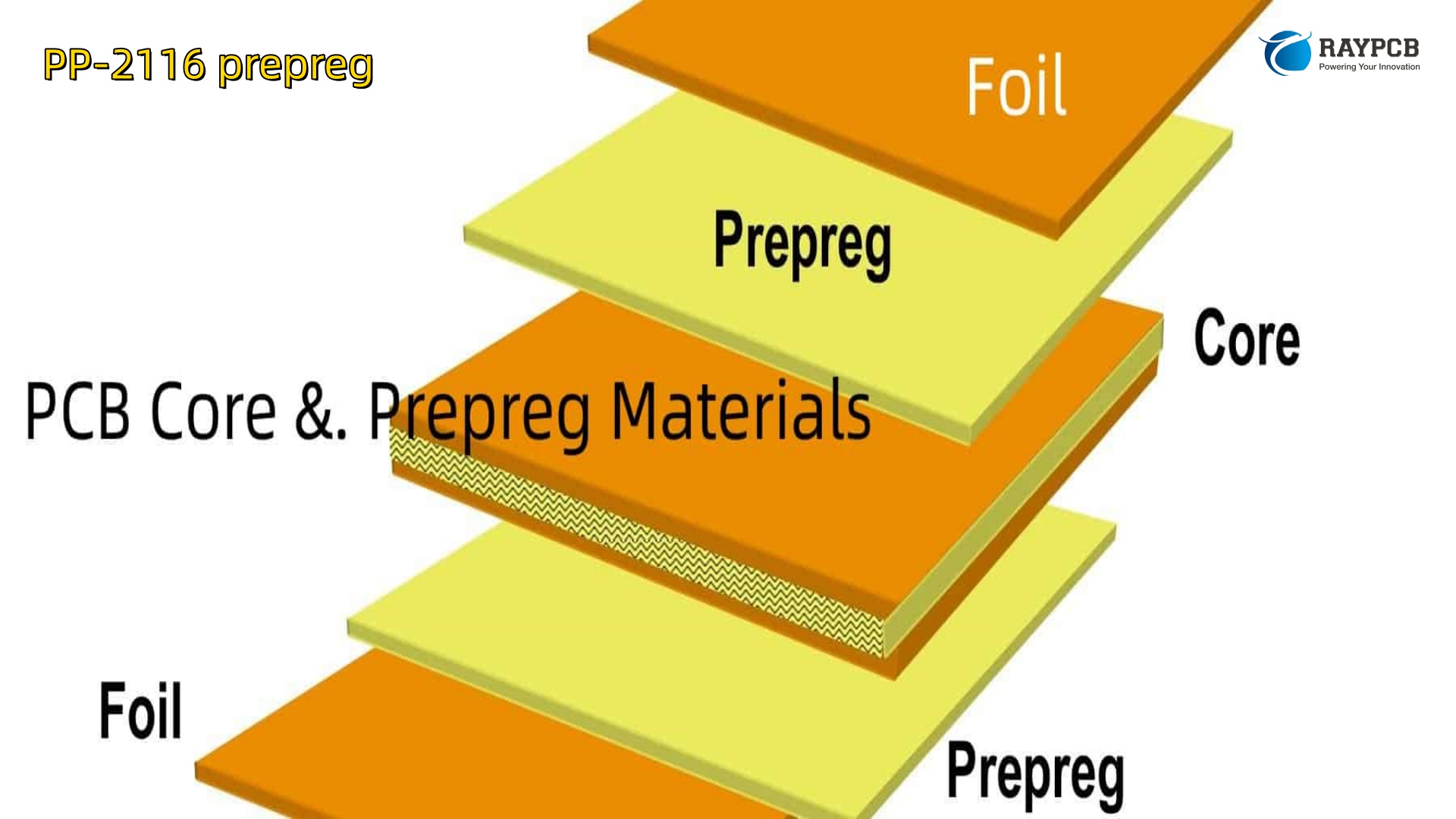
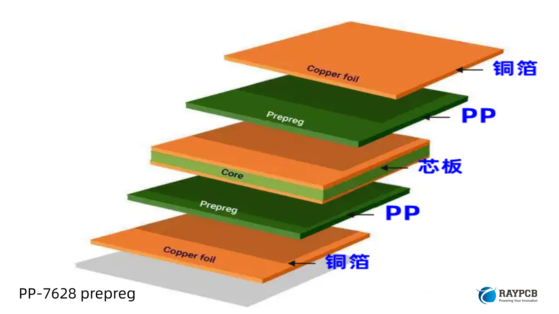
The resin impregnated into the glass fabric is in a semi-cured B-stage state. When heat and pressure are applied during lamination, that resin flows, bonds with adjacent copper layers or cores, then fully crosslinks into a hard dielectric. The entire layer integrity of your multilayer board depends on how well that process goes โ€” and PP-1080 thin prepreg is engineered to make it predictable.

PP-1080 Thin Prepreg: Key Technical Specifications

PP-1080 has a cured thickness range of approximately 60โ€“70 ฮผm and a dielectric constant (Er) of 3.2โ€“3.7, with resin content around 60%. However, these numbers vary across supplier product lines and resin content variants. The table below consolidates typical published values from leading laminate manufacturers:

PP-1080 Prepreg Specification Table

ParameterStandard RC (65%)High RC (68โ€“70%)Notes
Glass StyleIPC 1080IPC 1080Loose woven fiberglass
Cured Thickness0.075โ€“0.079 mm (3.0โ€“3.1 mil)0.085โ€“0.090 mm (3.3โ€“3.5 mil)Post-lamination value
Resin Content64โ€“65%68โ€“70%By weight
Dk @ 1 GHz3.52โ€“3.553.45โ€“3.49Higher RC = lower Dk
Df @ 1 GHz~0.0135~0.0138Standard FR-4 epoxy system
Tg (standard)130โ€“150ยฐC130โ€“150ยฐCHigh-Tg variants available
Moisture Absorption< 0.5%< 0.5%Per IPC-TM-650
Shelf Life6 months @ โ‰ค23ยฐC6 months @ โ‰ค23ยฐCDry, UV-protected storage

Engineer’s Note: For the 1080 glass style at 65% resin content, Dk reads approximately 3.55 at 100 MHz and 3.48 at 10 GHz; at 68% resin content, it drops to about 3.49 at 100 MHz and 3.41 at 10 GHz. Always pull the engineering data sheet from your laminate supplier โ€” not the marketing sheet โ€” when doing impedance calculations.

PP-1080 vs Other Common Prepreg Styles: Comparison Table

Understanding where PP-1080 thin prepreg sits in the ecosystem helps you make stack-up decisions faster. Here’s a side-by-side view:

PropertyPP-106PP-1080PP-2116PP-7628
Glass Style WeightUltra-lightLightweightMid-weightHeavy
Cured Thickness51โ€“61 ฮผm75โ€“90 ฮผm100โ€“132 ฮผm180โ€“200 ฮผm
Typical Resin Content72โ€“76%64โ€“70%52โ€“57%40โ€“45%
Dk @ 1 GHz (typical)~3.32~3.45โ€“3.52~4.40โ€“4.50~4.5โ€“4.6
Mechanical StrengthLowModerateGoodHigh
Resin FlowVery highHighMediumLow
Best ApplicationThin HDI layersThin build-up, HDIStandard multilayerThick structural layers
Relative CostModerateModerateLowLowest

Prepreg 1080 is thinner than Prepreg 2116 โ€” measuring around 60 to 90 microns versus 90 to 110 microns โ€” and also carries more resin, around 60โ€“68% by weight compared to about 50% for 2116. This changes how they bond and insulate.

Lightweight styles like 106 and 1080 offer higher resin content relative to glass, resulting in lower Dk values and smoother surfaces. They’re preferred for high-frequency applications where lower Dk improves signal propagation.

Why PP-1080 Thin Prepreg Is the Default for Thin PCB Build-Up

Controlled Dielectric Spacing in HDI Stack-Ups

When you’re building a 6-layer or 8-layer board in a 1.0 mm total thickness target, every micron matters. PP-1080 thin prepreg gives you a repeatable pressed thickness in the 75โ€“90 ฮผm range, which lets you hit tight dielectric spacing between signal layers and reference planes without stacking multiple plies.

Prepreg thickness directly determines the dielectric spacing between signal layers and reference planes. For controlled impedance designs, even a 0.5 mil thickness variation can shift impedance by 3โ€“5 ohms. At those tolerances, using a predictable, well-characterized material like PP-1080 is not optional โ€” it’s essential.

Impedance Control and Signal Integrity

Dk varies from 2.92 at 10 GHz for 1080 glass style to 3.19 at 10 GHz for 2116 glass style when comparing the same laminate system โ€” a Dk variation of roughly 3โ€“6% depending on resin content. For any design running differential pairs or controlled-impedance traces, this delta directly affects trace width calculations. PP-1080’s lower Dk versus 2116 allows for slightly wider traces at equivalent impedance targets, which is friendlier for fabrication yield.

Resin Flow Advantage in Complex Topographies

Inner layers with heavy copper pour create surface topology that thinner prepregs must fill completely to avoid voids. PP-1080’s higher resin content (65โ€“70%) gives it enough flow during lamination to fully encapsulate copper patterns โ€” critical for reliability in thermal cycling environments.

Compatibility with Laser Drilling in HDI

Flat glass cloth with high resin content such as 1035, 1067, and 1086 show excellent heat absorption properties for laser drilling. The same principle applies to PP-1080 โ€” its relatively high resin fraction and uniform weave minimize laser deflection during microvia formation. This makes PP-1080 thin prepreg a solid choice for HDI build-up layers where blind via formation by COโ‚‚ laser is part of the process.

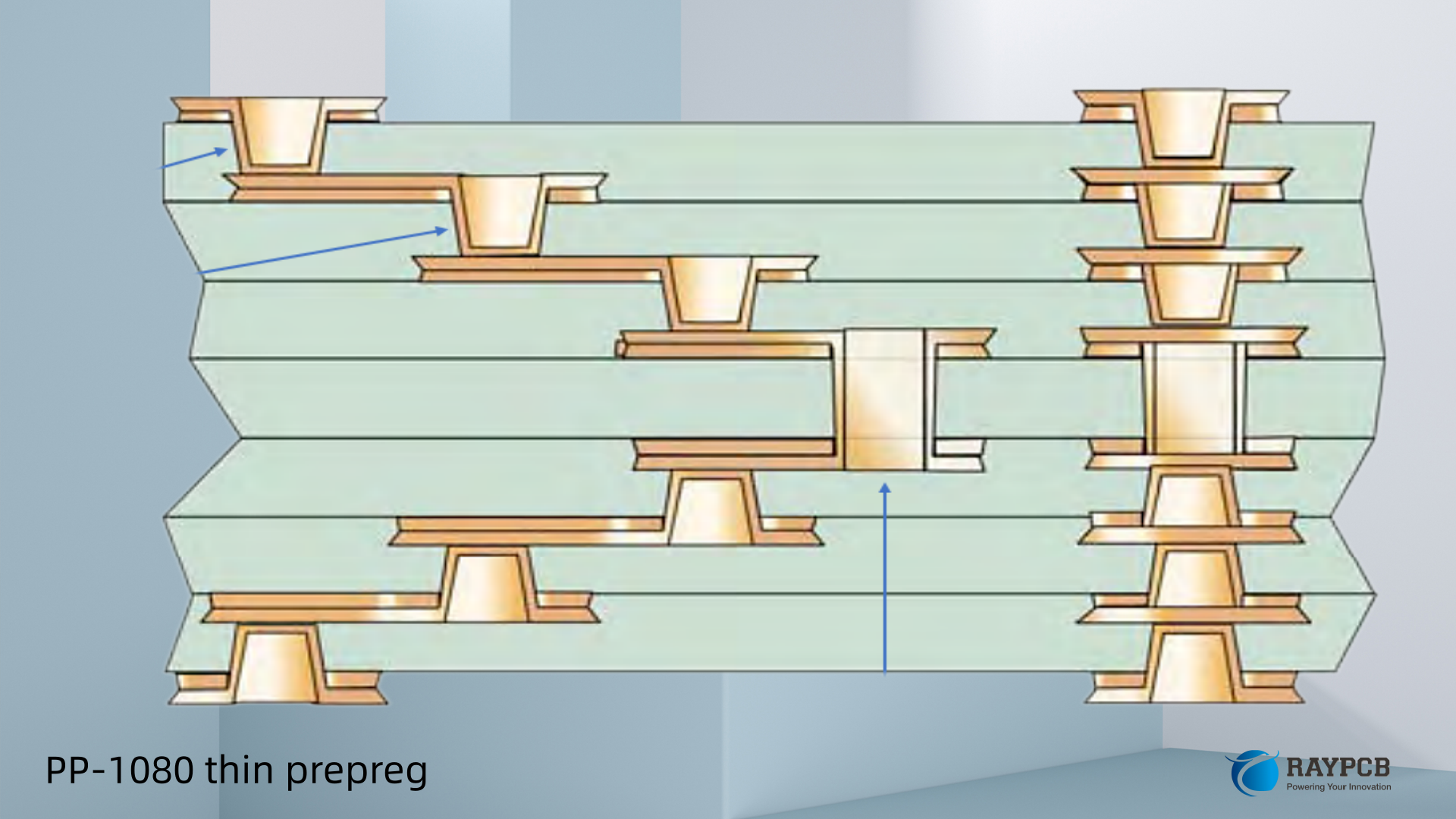
PP-1080 Thin Prepreg in Common PCB Stack-Up Configurations

4-Layer Thin Board (Total ~0.8 mm)

LayerMaterialThickness
L1 Copper1 oz Cu foil~35 ฮผm
Prepreg1ร— PP-1080 (HR)~90 ฮผm
CoreFR-4 0.36 mm core360 ฮผm
Prepreg1ร— PP-1080 (HR)~90 ฮผm
L4 Copper1 oz Cu foil~35 ฮผm
Solder mask (ร—2)LPI~25 ฮผm ร—2
Total ~660 ฮผm + plating

6-Layer Board with Thin Outer Dielectric (Total ~1.0 mm)

LayerMaterialThickness
L1Outer copper~35 ฮผm
PP2ร— PP-1080~150 ฮผm
CoreL2โ€“L3 core100 ฮผm
PP1ร— PP-1080~80 ฮผm
CoreCentral core360 ฮผm
PP1ร— PP-1080~80 ฮผm
CoreL4โ€“L5 core100 ฮผm
PP2ร— PP-1080~150 ฮผm
L6Outer copper~35 ฮผm
Total ~1090 ฮผm approx.

Adjusting to a single PP-1080 ply for intermediate interfaces and high-RC variants on outer layers gives you the flexibility to tune total board thickness with sub-100 ฮผm precision.

How to Select the Right PP-1080 Variant for Your Application

Not all PP-1080 thin prepregs are the same. Resin content, resin system (standard Tg vs. high Tg vs. halogen-free), and supplier all affect actual performance. Here’s a practical selection framework:

Selection Decision Table

Design RequirementRecommended PP-1080 Variant
Total board thickness < 0.8 mmPP-1080 Standard RC (65%), single ply
Controlled impedance ยฑ10%PP-1080 HR (68%), verify Dk from engineering datasheet
Lead-free assembly (โ‰ฅ260ยฐC reflow)PP-1080 High-Tg (Tg โ‰ฅ 170ยฐC)
Halogen-free / RoHS compliancePP-1080 HF grade (check supplier availability)
HDI with laser viasPP-1080 MR or HR โ€” higher resin aids laser drilling
Mixed-signal or RF (up to 6 GHz)PP-1080 with published Dk/Df table โ€” confirm at target frequency
High-reliability / automotivePP-1080 High-Tg + phenolic cure system

Material Supplier Datasheets Worth Bookmarking

Leading laminate manufacturers publish engineering-grade Dk/Df tables for 1080 glass style at multiple resin contents and frequencies. You should always use these rather than the single-number Dk on marketing sheets.
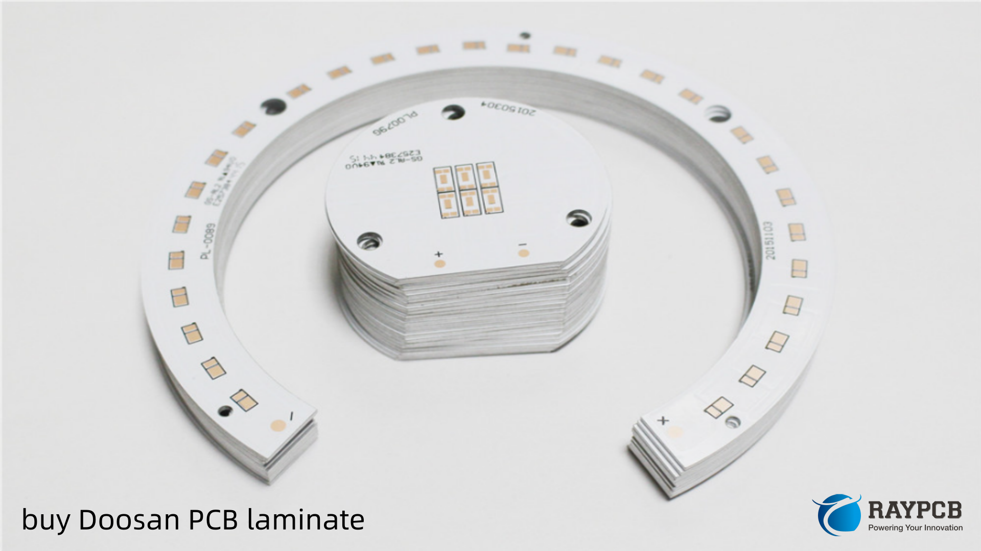
Doosan’s CCL product line โ€” documented at Doosan PCB โ€” includes 1080-compatible prepreg offerings with detailed thermal and electrical characterization data covering standard and high-Tg variants. Their materials are widely used in Korean and Asian PCB fabrication ecosystems where thin build-up tolerances are tightly controlled.

PP-1080 Prepreg Storage and Handling: What Gets Overlooked

A lot of field problems with PP-1080 thin prepreg trace back to storage or handling rather than material defects. The resin is in B-stage โ€” it’s chemically active and absorbs moisture from the air.

Before using prepregs in PCB manufacturing, they should be stored in special conditions: keep wrapped in damp-proof material to prevent moisture absorption that weakens bonding strength, and avoid UV rays and strong light.

Key handling rules for PP-1080 thin prepreg:

Storage temperature should be maintained at or below 23ยฐC with relative humidity under 50%. Shelf life runs approximately 3โ€“6 months from the manufacturing date depending on the resin system. Once a roll is opened, it should be used within the stated out-time window. Any prepreg exposed to moisture shows reduced resin flow during lamination, which causes voids and inconsistent dielectric thickness. Expired prepreg has advanced curing that reduces its ability to flow and bond properly, leading to poor adhesion, voids, delamination, and inconsistent thickness.

Useful Resources for PP-1080 Thin Prepreg Selection

ResourceLinkWhat It Contains
Isola IS415 Dk/Df Tableisola-group.comEngineering Dk/Df data for 1080 at multiple RC% and frequencies
IPC-4101 Specificationipc.orgIndustry standard for laminate and prepreg classifications
Altium Designer Materials Libraryaltium.comStack-up manager with prepreg material properties
Signal Integrity Journal โ€” Dk/Df Guidesignalintegrityjournal.comDeep dive on interpreting laminate data sheets
Sierra Circuits HDI Material Guideprotoexpress.comPractical HDI prepreg selection criteria
Doosan PCB MaterialsDoosan PCBDoosan CCL and prepreg product data including 1080-compatible grades
PCBSync Prepreg Guidepcbsync.comComprehensive practical prepreg selection guide

5 Frequently Asked Questions About PP-1080 Thin Prepreg

1. Can I use a single ply of PP-1080 between cores, or do I need two plies?

A single ply of PP-1080 thin prepreg (high-resin variant at ~90 ฮผm pressed) is often sufficient for inner-layer interfaces with moderate copper weight (ยฝ oz to 1 oz). However, on interfaces with heavy copper fill (2 oz or above), two plies are recommended to ensure complete resin fill of copper topology and avoid voids. Always confirm with your fabricator’s design rules โ€” some fabs mandate minimum ply counts between adjacent copper layers.

2. How does PP-1080 perform at frequencies above 5 GHz?

At 10 GHz, the 1080 glass style at 65% resin content shows a Dk of approximately 3.48 and a Df around 0.0143. This is acceptable for many digital high-speed designs but may be marginal for pure RF or mmWave applications. If you’re pushing past 10 GHz, consider low-loss prepreg systems (PTFE-based or hydrocarbon ceramic) with 1080-style glass for mechanical support, rather than standard FR-4 epoxy prepreg.

3. Is PP-1080 thin prepreg compatible with sequential lamination in HDI builds?

Yes โ€” PP-1080 is widely used in 1+N+1 and 2+N+2 HDI build-up constructions. Its high resin content supports good adhesion in the sequential press cycles, and its thickness is compatible with microvia aspect ratios achievable by COโ‚‚ laser drilling. Confirm that your chosen variant’s Tg is appropriate for the cumulative thermal exposure across multiple lamination cycles.

4. What’s the difference between standard RC and high RC variants for thin PCB purposes?

In short: standard RC (around 64โ€“65%) gives you a thinner pressed result (~75โ€“80 ฮผm), while high RC (68โ€“70%) results in a slightly thicker pressed sheet (~85โ€“90 ฮผm) but with lower Dk due to the higher resin fraction. For the thinnest possible build-up, use standard RC. For better impedance control and laser via compatibility, high RC is preferred. Resin content typically ranges 65โ€“75% for 106 and 1080 styles, which are used to bond inner layer cores together in thin build-up constructions.

5. Can I mix PP-1080 and PP-2116 in the same stack-up?

Mixing prepreg types is common โ€” for example, using 1080 prepreg for critical high-speed signal layers and 7628 for non-critical power plane separation. Just ensure CTE compatibility and verify Dk values for each layer in your impedance calculations. The same logic applies to mixing 1080 and 2116. Just be careful: Dk mismatch between layers adds modeling complexity, so always run your impedance tool with layer-specific Dk values rather than a single board-level number.

Summary: When PP-1080 Thin Prepreg Is the Right Call

PP-1080 thin prepreg hits a sweet spot that few other glass styles can match: thin enough for compact build-ups, resin-rich enough for reliable bonding, and electrically well-characterized across the frequency range most PCB engineers work in. Its Dk in the 3.45โ€“3.55 range (depending on resin content) makes impedance calculation straightforward, and its compatibility with laser drilling keeps it relevant in HDI designs.

Use PP-1080 thin prepreg when you’re working with total board thicknesses below 1.6 mm, when you need controlled impedance layers with predictable dielectric spacing, when your design involves HDI microvia build-up, or when lead-free assembly demand a high-Tg variant of the same base fabric style.

Where it’s not the best fit: ultra-high-frequency designs above 10 GHz (consider PTFE or hydrocarbon laminates), or applications where dimensional stability under heavy copper flood is the primary concern (2116 or 7628 may be better).

Pull your supplier’s engineering Dk/Df table, cross-check resin content against your stack-up model, and confirm pressed thickness with your fabricator before locking down the design. That three-step process eliminates most PP-1080 selection mistakes before they reach the production floor.

PP-2116 Prepreg: Why It’s the Standard Choice for Build-Up Layers

Learn why PP-2116 prepreg is the standard choice for PCB build-up layers. This engineer’s guide covers key specs, stack-up examples, resin grades (SR/MR/HR), storage rules, comparison tables vs. 1080 and 7628, and useful datasheets โ€” everything you need to make the right material call.

If you’ve been doing multilayer PCB stack-up work long enough, you already know that material selection is rarely glamorous โ€” but it matters enormously. One material that comes up in almost every build-up conversation is PP-2116 prepreg. Walk into any mid-to-high volume PCB fab and the odds are strong that 2116 is sitting in the lamination room as the default go-to. This guide breaks down exactly why that is, what the numbers mean, and when you should โ€” or shouldn’t โ€” reach for it.

What Is PP-2116 Prepreg?

Prepreg (short for “pre-impregnated”) is fiberglass cloth saturated with a partially cured epoxy resin system, held in what’s called a B-stage cure state. It stays pliable and slightly tacky until you hit it with heat and pressure in the lamination press โ€” at which point the resin flows, fills the copper relief, and cures into a solid dielectric layer bonding everything together.

The number “2116” refers to the IPC glass fabric style โ€” a mid-weight E-glass weave with a specific thread count and construction. Mid-weight styles like 2116 provide a balance between cost, mechanical properties, and electrical performance, making them workhorses for most standard multilayer PCBs.

Think of it as the 18-gauge wire of the PCB materials world โ€” not the thinnest, not the thickest, but reliable enough to cover the majority of real-world applications without breaking the bank.

PP-2116 Prepreg Key Technical Specifications

PP 2116 has a thickness range of 90โ€“110 ฮผm, a dielectric constant (Er) of 3.6โ€“3.8, and a resin content of approximately 50%. These values shift slightly depending on the supplier and resin grade, so always verify against the specific datasheet you’re designing to.

ParameterPP-2116 (Typical)PP-1080 (Typical)PP-7628 (Typical)
Glass Fabric Style211610807628
Cured Thickness (ฮผm)90โ€“11060โ€“70170โ€“190
Resin Content (%)~50~60~45
Dk (Er) @ 1 GHz3.9โ€“4.2~3.54.1โ€“4.6
Dissipation Factor (Df)~0.020~0.018~0.022
Typical ApplicationStandard build-up layersHigh-density / high-speedThick filler / cost-sensitive
Relative CostMediumMedium-LowLow

Resin grades are also available within the 2116 style:

GradeResin ContentFlow BehaviorBest Used For
SR (Standard Resin)~50โ€“52%Low flowPlane-to-plane bonding, stable geometry
MR (Medium Resin)~52โ€“56%ModerateGeneral signal layer builds
HR (High Resin)~56โ€“60%High flowHeavy inner copper (2 oz+), filling etched areas

2116SR prepreg (โ‰ˆ50% resin) is ideal for plane-to-plane bonding applications, while the HR grade is better suited where you need aggressive resin fill around thick copper traces.

Why PP-2116 Prepreg Dominates Build-Up Layers

Balanced Dielectric Thickness for Impedance Control

One of the most practical reasons 2116 shows up in almost every standard stack-up is the dielectric thickness it produces after pressing. For lower routing densities and higher current requirements, 2116 and 7628 allow for traces 8 to 14 mils in width. That range sits comfortably in the sweet spot for most controlled impedance designs โ€” 50ฮฉ microstrip and stripline are both achievable without exotic trace widths.

In a typical 4-layer 1.6mm board, the stack-up using 1 oz Cu and two sheets of 2116 pre-preg on each side of the core would produce a spacing between the top layer and the signal core finishing at about 9.3 mils. That’s a well-characterized, repeatable geometry that makes impedance modeling reliable.

Industry-Standard Stack-Up Compatibility

In standard pool fabrication, prepreg types including PR2116 (120 ฮผm) are among the standard prepregs used for predefined build-ups alongside PR1080 (70 ฮผm) and PR7628 (180 ฮผm). The fact that major PCB pool services carry 2116 as a standard material means your design is more likely to be manufactured without substitution flags or material surcharges โ€” important when you’re doing quick-turns.

Mechanical Stability and Resin Flow

The 2116 weave is tight enough to give you good dimensional stability during pressing, while still providing enough resin to fill relief around inner-layer copper. This balance is why 2116SR is preferred for plane-to-plane bonding applications โ€” the controlled flow reduces squeeze-out and keeps dielectric thickness consistent across the panel.

Compatibility with Doosan PCB Materials

Doosan PCB materials, including their popular DS-7409 series, are widely used with the 2116 glass style. Doosan’s epoxy systems are formulated to work predictably within standard 2116 press cycles, which makes them a common choice in fabrication shops already qualified on FR-4 processes. When specifying Doosan-based laminates, the 2116 prepreg format integrates directly into existing lay-up procedures without requiring changes to press recipes or oxide treatment lines.

PP-2116 vs. Other Prepreg Styles: When to Switch

Choosing the right prepreg isn’t just about picking the default โ€” here’s how to think through alternatives:

SituationRecommended PrepregReason
Standard 4โ€“8 layer FR-4 board2116Best all-round balance
High-speed signal layers (>5 GHz)1080 or 3313Lower Dk, smoother surface, reduced fiber weave effect
Heavy copper (2 oz+) inner layers2116HR or 1080HRHigher resin fill to cover copper relief
Very thick filler dielectric7628Thicker single-ply, lower cost
Cost-driven, low-layer-count board7628Lower material cost
Controlled impedance on thin builds1080Thinner pressed dielectric

Lightweight styles like 1080 are preferred for high-frequency applications where lower Dk improves signal propagation, so if you’re routing >5 GHz differential pairs, moving to a 1080-based dielectric on those critical layers makes sense โ€” while keeping 2116 everywhere else.

PP-2116 Prepreg in Multilayer Stack-Up Design

4-Layer Board Stack-Up Example

A common 1.6mm 4-layer build using 2116:

LayerMaterialThickness
L1 (Top)1 oz Cu foil35 ฮผm
Dielectric2ร— PP-2116~200โ€“220 ฮผm
L2Inner copper (etched)17 ฮผm
CoreFR-4 core~900 ฮผm
L3Inner copper (etched)17 ฮผm
Dielectric2ร— PP-2116~200โ€“220 ฮผm
L4 (Bottom)1 oz Cu foil35 ฮผm

6-Layer Board Stack-Up Example

For a 6-layer 1.6mm design, 2116 is typically used for the outer build-up dielectrics while thinner 1080 or the core itself handles the inner signal spacing:

LayerMaterialNotes
L1 / L6 outer dielectric1โ€“2ร— PP-2116Controls outer microstrip impedance
Inner signal dielectrics1080 or thin coreTighter spacing for stripline control
L3/L4 separationCore materialProvides rigid center

Engineer’s tip: Never stack more than 3 sheets of prepreg between layers. In practice, it is not recommended to stack more than 3 sheets of prepreg together โ€” resin squeeze-out becomes uncontrollable and you’ll see thickness variation across the panel.

Storage and Handling: Don’t Wreck Your Material

Before using prepregs for PCB manufacturing, they should be stored in special conditions: beware of moisture, always keep wrapped in damp-proof material. Keeping in normal conditions, prepreg might absorb moisture and its bonding strength would be weakened. Avoid UV-rays and strong light.

Practically speaking, your PP-2116 rolls should live in a temperature-controlled, humidity-monitored storage room โ€” ideally below 23ยฐC and at 40โ€“60% RH. If the prepreg is not consumed within 48 hours after opening the vacuum package, it is recommended that the bags be resealed. Expired prepreg that’s absorbed moisture will delaminate โ€” often intermittently, which is the worst kind of failure to chase down.

Standard shelf life for most PP-2116 materials is 3โ€“6 months from the manufacture date, depending on the supplier’s resin system. Always check the date stamp on the roll end label before pulling it for a production run.

Useful Resources for PP-2116 Prepreg

Here are some reference links engineers frequently use when working with 2116 prepreg stack-ups:

Frequently Asked Questions About PP-2116 Prepreg

Q1: Can I substitute PP-2116 with PP-2125 in my existing stack-up?

Not directly. The thickness of 2116 differs from 2125 by approximately 20 ฮผm โ€” and in a standard 6-layer board that used 7 sheets of this type, the thickness difference resulted in an unexpected, often too-thick final board. Always recalculate your stack-up if switching between these styles.

Q2: What Dk value should I use for PP-2116 in impedance calculations?

Use post-lamination Dk values from your specific supplier’s datasheet โ€” not the raw prepreg Dk. The dielectric constant Er for 1ร— Prepreg 2116 is approximately 4.20 as a typical starting point, but this changes based on copper coverage on adjacent layers. Always run calculations with both signal-adjacent (lower Dk) and ground-adjacent (higher Dk) values.

Q3: How many sheets of PP-2116 can I use between layers?

A maximum of 3 sheets is the practical limit. Beyond that, resin flow becomes difficult to control and you’ll see dielectric thickness inconsistency. Two sheets of 2116 is most common for outer build-up layers on standard 4- and 6-layer boards.

Q4: Is PP-2116 suitable for high-speed designs?

It’s usable up to around 5 GHz in most situations, but the fiber weave pattern can cause periodic Dk variations along a trace โ€” known as fiber weave effect. For critical >5 GHz differential pairs, consider moving to 1080 or mechanically rotating/offsetting the weave at 45ยฐ to reduce this effect.

Q5: Does PP-2116 come in halogen-free versions?

Yes. Most major suppliers โ€” including Isola, Shengyi, Panasonic (Megtron), and Doosan โ€” offer halogen-free 2116 prepreg meeting IEC 61249-2-21. These use phosphorus-based flame retardants and typically carry slightly different Dk/Df values compared to standard FR-4, so update your impedance models accordingly.

Meta Description Suggestion:

Learn why PP-2116 prepreg is the standard choice for PCB build-up layers. This engineer’s guide covers key specs, stack-up examples, resin grades (SR/MR/HR), storage rules, comparison tables vs. 1080 and 7628, and useful datasheets โ€” everything you need to make the right material call.

(Character count: ~280 โ€” trim to ~155 characters for Google if needed)

Shorter version (155 chars): PP-2116 prepreg is the go-to choice for multilayer PCB build-up layers. Explore specs, stack-up examples, resin grades, and expert selection tips in this guide.

PP-7628 Prepreg: Glass Style, Resin Content & MLB Applications

Learn everything about PP-7628 prepreg โ€” glass style construction, resin content grades (SR/MR/HR), key dielectric specs, and how to use it correctly in multilayer PCB stackups. Written from a PCB engineering perspective with spec tables, storage tips, and application guidance.

If you’ve spent any time reviewing PCB stackup documentation, you’ve almost certainly run into PP-7628 prepreg. It’s one of the most widely used bonding materials in multilayer board fabrication, and for good reason โ€” it’s thick, cost-effective, and mechanically robust. But if you’re just pulling it into your stackup because “everyone uses it,” you might be leaving performance on the table or running into trouble you don’t expect.

This guide breaks down exactly what PP-7628 prepreg is, what its glass style and resin content actually mean for your board, and where it fits โ€” and doesn’t fit โ€” in multilayer PCB (MLB) applications.

What Is PP-7628 Prepreg?

PP-7628 prepreg (also written as 7628 prepreg or prepreg 7628) is a B-stage composite material made of woven E-glass fabric pre-impregnated with a partially cured epoxy resin system. The designation “7628” refers specifically to the IPC-recognized glass fabric style โ€” the weave pattern, yarn density, and construction of the fiberglass cloth.

In PCB manufacturing, prepreg sits between core layers or between a core and copper foil. During the lamination press cycle, heat activates the resin, which flows, fills in around etched copper features, and then fully cures โ€” permanently bonding the stack into a solid multilayer structure. Once cured, it becomes the dielectric layer separating your copper planes and signal layers.

The “PP” simply stands for pre-preg or pre-impregnated, and the number tells you which glass cloth was used. Other common types include PP-106, PP-1080, and PP-2116. Each has its own weight, thickness, and resin pickup characteristics.

PP-7628 Glass Style: What the Number Tells You

The 7628 glass style is one of the heaviest and most tightly woven fabrics used in standard FR-4 PCB production. The weave is dense and uses thicker yarns compared to lighter styles like 1080 or 106.

The glass weave in 7628 prepreg is tight โ€” controlled with a loom during manufacturing โ€” and the final electromagnetic properties, including dispersion, losses, and fiber weave effects observed by signals in the board, are determined by the gaps and homogeneity of that weave.

What this means in practice: 7628 has less resin relative to glass compared to lighter styles, which gives it excellent dimensional stability and mechanical stiffness. However, the coarser surface texture is less forgiving for fine features and high-speed signals.

PP-7628 Weave Characteristics vs Other Glass Styles

Glass StyleWeave TypeFabric Weight (g/mยฒ)Typical Application
106Very loose~24HDI, ultra-thin, high-frequency
1080Loose~48Fine-pitch, high-frequency
2116Medium~104General multilayer, balanced performance
7628Tight/Heavy~203Thick MLB, power layers, cost-sensitive designs

PP-7628 Resin Content: SR, MR, and HR Explained

Resin content (RC%) is the weight percentage of resin relative to the total prepreg weight. For PP-7628, the standard resin content sits at around 42โ€“48% โ€” noticeably lower than lighter styles like 1080 (which can reach 60โ€“70%).

Typical resin content ranges for heavy glass cloth like 7628 run approximately 40โ€“50%, while lighter styles like 106 and 1080, typically used to bond inner layer cores together, run 65โ€“75%.

Within the 7628 style, you’ll encounter three resin content tiers:

PP-7628 Resin Content Variants

VariantResin ContentFlow BehaviorBest Use Case
SR (Standard Resin)~42%Low flowPlane-to-plane bonding, flat surfaces
MR (Medium Resin)~45%Moderate flowGeneral MLB dielectric layers
HR (High Resin)~48โ€“50%Higher flowThick copper (2oz+) inner layers with deep etching

Choosing the right resin content class ensures full copper filling without excessive squeeze-out, helping maintain dielectric consistency and prevent lamination voids.

Increasing resin content in 7628 also shifts the dielectric constant slightly. Higher RC means more resin and less glass, which generally lowers Dk โ€” important if you’re running impedance-controlled traces through layers using 7628 as the dielectric.

PP-7628 Prepreg Key Specifications

Here’s a reference table for PP-7628 based on standard FR-4 epoxy systems:

ParameterTypical ValueNotes
Cured Thickness170โ€“190 ยตm (0.0067โ€“0.0075 in)Varies by RC and lamination pressure
Dielectric Constant (Dk) at 1 GHz4.1โ€“4.6Higher than lighter styles
Dissipation Factor (Df) at 1 GHz~0.02Standard FR-4 range
Resin Content42โ€“48%Depends on SR/MR/HR grade
Glass Fabric Weight~203 g/mยฒHeaviest standard PCB style
Tg (Standard FR-4)130โ€“170ยฐCHigh-Tg and halogen-free grades available

PP-7628 has a thickness range of 170โ€“190 ยตm and an Er (dielectric constant) of 4.1โ€“4.6. That’s the thickest single-ply prepreg in the standard FR-4 lineup, which makes it extremely useful when you need to hit a target board thickness without stacking multiple thinner plies.

PP-7628 Prepreg in Multilayer Board (MLB) Applications

Where PP-7628 Excels

PP-7628 earns its place in multilayer stackups primarily because of its mechanical properties and cost efficiency. In production, it’s a go-to choice for:

Thick MLB constructions (6โ€“16+ layers): When you need board thickness approaching 1.6mm or beyond, 7628 lets you reach target dimensions with fewer plies than 2116 or 1080. This reduces material cost and press time.

Power plane separation: Separating power and ground planes doesn’t require premium dielectric performance. 7628 SR at low cost fills this role well โ€” good adhesion, stable thickness, no need for low-Dk or low-Df properties.

Industrial and commercial-grade electronics: Telecom backplanes, industrial control boards, and general computing hardware where signal frequencies stay under 1โ€“2 GHz are well-served by 7628 prepreg.

Cost-sensitive designs: Heavyweight 7628 prepreg costs less and provides excellent dimensional stability, making it a practical choice for non-critical layers where controlled impedance or high-speed designs are not the priority.

Doosan PCB laminates, for example, often utilize 7628-based prepreg systems in standard MLB stackups, combining it with matched core materials to maintain consistent dielectric properties through the press cycle.

Where PP-7628 Prepreg Falls Short

The thicker glass fibers in 7628 can deflect small drill bits, causing hole quality issues in HDI applications. For any board with laser vias, fine drill patterns under 0.2mm, or HDI build-up layers, 7628 is not the right call.

For high-speed digital signals above 2โ€“3 GHz, 7628’s higher Dk and coarser weave introduce signal integrity challenges including fiber weave effect, which causes differential skew between closely routed pairs. Lighter styles like 1080 or 2116 with tighter resin control are better suited there.

Mixing PP-7628 with Other Prepreg Styles

It’s common practice in MLB fabrication to combine prepreg types within the same stackup. A typical approach:

  • Use 1080 or 2116ย for signal-sensitive dielectric layers where Dk consistency and smooth surface matter
  • Use 7628ย for outer dielectric layers or plane separations where cost and thickness matter more

Just ensure CTE compatibility and verify Dk values for each layer in your impedance calculations when mixing prepreg types.

PP-7628 Prepreg Storage and Handling

Prepreg shelf life matters more than most engineers think. Expired or improperly stored material has advanced its cure state, reducing resin flow during lamination and causing adhesion failures, voids, or inconsistent pressed thickness.

Keep PP-7628 prepreg:

  • In a temperature-controlled environment (typically 5โ€“23ยฐC)
  • Wrapped in moisture-proof packaging at all times
  • Away from UV light and strong artificial light sources
  • Within the manufacturer’s stated shelf life (usually 3โ€“6 months from production date)

Before production runs with questionable material, always conduct a flow test on sample coupons.

Useful Resources for PP-7628 Prepreg

ResourceDescriptionLink
IPC-4101Standard specification for base materials used in rigid PCBs, including prepregIPC.org
Isola Prepreg Data SheetsDk/Df tables for IS410, IS420 across glass styles including 7628Isola-Group.com
Ventec VT-47 / VT-441 DataProcess guides and prepreg specs for halogen-free 7628 variantsVentec-Group.com
Shengyi S1141 Data SheetWidely used FR-4 with 7628 prepreg specs, common in Asia-based fabsShengyi-tech.com
JLCPCB Impedance CalculatorStackup tool referencing 7628 layer thicknesses for impedance estimationJLCPCB.com/impedance

FAQs About PP-7628 Prepreg

Q1: Can I use a single ply of PP-7628 as the only prepreg between two cores?

Yes, a single ply of 7628 is actually one of its advantages โ€” at 170โ€“190 ยตm cured thickness, one sheet gives you meaningful dielectric separation without stacking multiple thinner plies. However, for very heavy copper layers (3oz+), consider HR grade or adding an additional ply of a thinner style like 2116 to ensure full void-free resin fill around the copper features.

Q2: What is the Dk of PP-7628 prepreg, and does it vary?

The nominal Dk of standard FR-4 7628 prepreg runs from about 4.1 to 4.6 at 1 GHz, depending on resin content, supplier, and test method. Higher resin content slightly lowers Dk. Always use your fab’s actual measured Dk values โ€” not just datasheet nominals โ€” when running impedance calculations.

Q3: Is PP-7628 suitable for lead-free assembly processes?

Standard Tg 7628 prepreg (Tg ~130ยฐC) can be marginal for lead-free reflow profiles, which peak at 260ยฐC. For lead-free processes, use high-Tg (Tg 170ยฐC+) or mid-Tg 7628 versions with a higher decomposition temperature (Td > 300ยฐC) to avoid measling, delamination, or CAF failures after assembly.

Q4: Why does my board warp when using PP-7628 in the outer layers?

7628’s heavy glass construction provides good in-plane stability, but asymmetric stackups โ€” more 7628 on one side than the other โ€” can cause warping as the board cools from the press. Always design your stackup with symmetric prepreg placement around the center core to balance thermal expansion and minimize bow and twist.

Q5: How does PP-7628 compare to PP-2116 for a standard 4-layer board?

For a 4-layer, 1.6mm board, 7628 is a common and cost-effective choice for the outer prepreg layers. It easily achieves target thickness in a single ply. PP-2116 gives slightly better signal integrity (lower Dk, smoother surface) and is preferred when layer 1 or 4 carry high-speed signals. If your signals are under 1 GHz and cost matters, 7628 SR or MR is a practical default.

Meta Description Suggestion:

“Learn everything about PP-7628 prepreg โ€” glass style construction, resin content grades (SR/MR/HR), key dielectric specs, and how to use it correctly in multilayer PCB stackups. Written from a PCB engineering perspective with spec tables, storage tips, and application guidance.”

(Character count: ~248 โ€” trim to 155โ€“160 characters for Yoast green status. Suggested shortened version:)

“PP-7628 prepreg explained for PCB engineers: glass style, resin content grades, dielectric specs, and multilayer board application guide with comparison tables.” (159 characters)

PP-7628HF Halogen-Free Prepreg: MLB Green Compliance Guide

Complete PP-7628HF prepreg guide: specs, halogen limits (IEC 61249-2-21), MLB stack-up examples, green compliance checklist, and processing tips for halogen-free PCB production.

If you’ve been quoting multilayer boards for EU, Japanese, or major US OEM supply chains lately, there’s a good chance someone on the sourcing side has asked the question: “Is this halogen-free?” The answer usually comes down to one material decision made early in the stack-up process โ€” the prepreg. For thick structural interfaces in MLB (multilayer board) construction, PP-7628HF prepreg is the halogen-free workhorse that satisfies both mechanical requirements and green compliance mandates without forcing you into exotic resin systems.

This guide covers what PP-7628HF prepreg actually is, how its specifications compare to standard 7628 and other glass styles, what “green compliance” requires in real regulatory terms, and how to specify and validate it correctly for production.

What Is PP-7628HF Prepreg and Why the “HF” Designation Matters

The “7628” in the name refers to the IPC glass fabric style โ€” a tightly woven E-glass construction that produces one of the heaviest, thickest, and most dimensionally stable prepreg layers available in standard PCB fabrication. The tight weave gives 7628 excellent mechanical strength and keeps dimensional variation in the X-Y plane well below 0.5%, which matters a lot in large-panel MLB manufacturing where registration tolerance across 20+ layers is cumulative.

The “HF” suffix stands for Halogen-Free. It signals that the epoxy resin system infused into the glass fabric does not rely on tetrabromobisphenol A (TBBPA) โ€” the brominated flame retardant used in conventional FR-4 โ€” for its flame retardancy. Instead, PP-7628HF prepreg uses phosphorus-nitrogen (P-N) compound systems or inorganic flame retardants that achieve UL 94 V-0 flammability ratings without introducing chlorine or bromine above threshold limits.

This distinction matters for compliance. Standard FR-4, while legal under RoHS as currently written, still contains brominated epoxy resin that releases hydrogen bromide (HBr) when burned. Multiple OEMs โ€” particularly in consumer electronics, automotive, and telecom โ€” now require total bromine content below 900 ppm at the laminate and prepreg level, which standard FR-4 cannot meet.

PP-7628HF Prepreg: Key Technical Specifications

PP-7628 has a cured thickness of 170โ€“190 ฮผm and Er values in the range of 4.1โ€“4.6, with resin content around 45%. The HF variant shares the same glass construction but substitutes the resin chemistry. Key differences between the standard and HF variants are highlighted in the table below.

PP-7628HF Specification Table

ParameterStandard PP-7628PP-7628HF (Halogen-Free)Notes
Glass StyleIPC 7628IPC 7628Tight woven E-glass
Resin SystemBrominated epoxy (TBBPA)Phosphorus-nitrogen / modified epoxyHF uses P-N flame retardant
Cured Thickness170โ€“200 ฮผm (6.7โ€“7.9 mil)175โ€“200 ฮผm (6.9โ€“7.9 mil)Slightly higher RC possible
Resin Content40โ€“45%42โ€“48%HF resin may carry slightly more filler
Dk @ 1 GHz4.4โ€“4.64.3โ€“4.5P-N resin slightly lowers Dk
Df @ 1 GHz~0.020~0.018โ€“0.021Comparable; check supplier data
Tg (standard)130โ€“150ยฐC140โ€“170ยฐCHF variants often run higher Tg
Bromine (Br)18,000โ€“22,000 ppm< 900 ppmHF meets IEC 61249-2-21
Chlorine (Cl)< 200 ppm< 900 ppmBoth well within total limit
Total Halogens~20,000 ppm< 1,500 ppmKey compliance threshold
UL 94 RatingV-0V-0Same flame class
Moisture Absorption< 0.5%< 0.4%HF often shows slight improvement
Shelf Life6 months @ โ‰ค23ยฐC6 months @ โ‰ค23ยฐCSame storage requirements

Engineer’s Note: PP-7628HF prepreg from different suppliers โ€” Shengyi, Isola, Ventec, Doosan โ€” will show different specific Dk/Df values due to their proprietary P-N resin systems. Always pull the engineering-grade Dk/Df table from the supplier, not the marketing sheet. One supplier’s 7628HF at 42% RC will have a different pressed Dk than another’s at 46% RC.

Green Compliance Standards That PP-7628HF Prepreg Must Satisfy

This is where a lot of engineers get confused. “Green compliance” is not a single standard โ€” it’s a stack of overlapping regulatory frameworks and OEM requirements, each with slightly different scope and thresholds. Here’s what actually applies to PP-7628HF prepreg selection:

Regulatory Compliance Framework Table

Standard / DirectiveScopeHalogen LimitPP-7628HF Status
IEC 61249-2-21PCB laminates and prepregsCl โ‰ค 900 ppm, Br โ‰ค 900 ppm, total โ‰ค 1500 ppmโœ… Compliant
JPCA-ES-01-2003Japanese electronics industrySame 9-9-15 ruleโœ… Compliant
EU RoHS DirectiveRestricts PBB and PBDE specificallyNo explicit 900 ppm rule โ€” bans specific BFRsโœ… Compliant (note: RoHS โ‰  halogen-free)
EU REACHChemical registration and restrictionSubstance-of-very-high-concern (SVHC) reportingโœ… Compliant with P-N systems
WEEE DirectiveEnd-of-life recyclabilityFacilitates safer e-waste processingโœ… Supports WEEE goals
IPC-WP/TR-584Industry white paper defining halogen-freeCodifies 9-9-15 rule, references IEC 61249-2-21โœ… Defines the baseline
UL 94 V-0FlammabilityNot a halogen standard โ€” flame performance onlyโœ… P-N systems achieve V-0

RoHS compliance does not equal halogen-free. The EU RoHS Directive banned two specific brominated flame retardants โ€” polybrominated biphenyls (PBB) and polybrominated diphenyl ethers (PBDE) โ€” but does not ban all brominated flame retardants. Many engineers confuse this and assume RoHS-compliant standard FR-4 is also halogen-free. It is not.

According to standards such as JPCA-ES-01-2003 and IEC 61249-2-21, a printed board is considered halogen-free if chlorine is no more than 900 ppm, bromine is no more than 900 ppm, and combined Cl + Br is no more than 1500 ppm. PP-7628HF prepreg is specifically engineered to meet all three thresholds across the entire laminated structure.

Why PP-7628HF Is the Go-To for MLB Structural Layers

Mechanical Strength and Dimensional Stability

Heavyweight styles like 7628 cost less and provide excellent dimensional stability, but their rougher surface and higher Dk make them less suitable for controlled impedance or high-speed designs. That’s actually the point โ€” PP-7628HF prepreg is not selected for signal integrity layers. It’s specified for power plane separation, board-thickening interfaces, and structural bonding layers in 8โ€“20+ layer MLB designs where dimensional stability and mechanical integrity under thermal cycling take priority over Dk precision.

In a 16-layer MLB, you might have four or five interfaces between inner cores where the only design requirement is mechanical bond strength, Z-axis CTE control, and fire-rating compliance. Using PP-7628HF at those interfaces delivers the required thickness per ply (~185 ฮผm), reduces layer count relative to using multiple thin plies, and costs less than 2116 or 1080 alternatives โ€” all while keeping the board halogen-free throughout.

Thermal Performance Advantage of HF Resin Systems

One underappreciated benefit of PP-7628HF prepreg is that the phosphorus-nitrogen resin systems used in HF materials typically deliver higher Tg than conventional DICY-cured FR-4 at similar cost. Modern halogen-free systems deliver high-Tg of 170โ€“200ยฐC and Df of 0.009โ€“0.012 at 1 GHz, enabling reliable performance across multiple reflow cycles.

For lead-free assembly โ€” where peak reflow temperatures hit 255โ€“260ยฐC โ€” having your structural prepreg at Tg โ‰ฅ 150ยฐC (ideally 170ยฐC) provides meaningful safety margin against delamination. PP-7628HF in phenolic-cured or P-N cure systems often reaches Tg 150โ€“175ยฐC, which is 20โ€“40ยฐC better than DICY-cured standard FR-4.

Cost Position Relative to Other HF Options

Not all halogen-free prepregs are created equal in cost. PP-7628HF sits at the lower end of the HF prepreg cost curve because the 7628 glass fabric itself is the lowest-cost style, and high-volume availability of HF resin systems for 7628 has brought pricing down significantly over the past decade. The cost premium over standard 7628 runs approximately 8โ€“18% depending on supplier and volume, which is far more palatable than switching to halogen-free 1080 or 2116 variants for every layer in a thick MLB.

PP-7628HF Prepreg in a Typical MLB Stack-Up

Below is a representative 10-layer MLB stack-up showing where PP-7628HF prepreg is used for structural interfaces:

10-Layer MLB Stack-Up with PP-7628HF (Total ~2.4 mm)

LayerMaterialThicknessPurpose
L11 oz Cu foil35 ฮผmSignal / ground
PP2ร— PP-7628HF (42% RC)~370 ฮผmOuter structural bond
CoreL2โ€“L3 FR-4 HF core100 ฮผmInner signal pair
PP1ร— PP-7628HF (46% RC)~190 ฮผmPower plane separation
CoreL4โ€“L5 FR-4 HF core100 ฮผmPower / ground pair
PP1ร— PP-7628HF (46% RC)~190 ฮผmCentral structural
CoreCentral FR-4 HF core800 ฮผmMechanical backbone
PP1ร— PP-7628HF (46% RC)~190 ฮผmLower power separation
CoreL6โ€“L7 FR-4 HF core100 ฮผmPower / ground pair
PP1ร— PP-7628HF (46% RC)~190 ฮผmInner signal separation
CoreL8โ€“L9 FR-4 HF core100 ฮผmInner signal pair
PP2ร— PP-7628HF (42% RC)~370 ฮผmLower structural bond
L101 oz Cu foil35 ฮผmSignal / ground
Total ~2.37 mmยฑ10% lamination tolerance

In this construction, PP-7628HF handles all structural bonding interfaces while the tight-tolerance signal layers use thin HF prepreg (1080HF or 2116HF) to maintain impedance control. This mixed approach gives you full green compliance on every layer while keeping material cost under control.

How to Specify PP-7628HF Prepreg Correctly

Getting the spec wrong on your fab drawing is one of the most common ways halogen-free compliance fails in the supply chain. Here’s what your fabrication notes need to include:

PP-7628HF Stack-Up Specification Checklist

Specification FieldWhat to StateWhy It Matters
Glass StyleIPC 7628Locks in fabric construction
Resin SystemHalogen-free (P-N or phosphorus-based)Prevents substitution with TBBPA resin
Compliance StandardIEC 61249-2-21States the 9-9-15 threshold requirement
Bromine LimitBr < 900 ppmExplicit measurement threshold
Chlorine LimitCl < 900 ppmExplicit measurement threshold
Combined HalogensCl + Br < 1500 ppmTotal threshold per IEC standard
Tg Minimumโ‰ฅ 150ยฐC (or 170ยฐC for lead-free)Thermal reliability requirement
Test MethodEN 14582 or ICP-MSSpecifies how halogen content is verified
Material CertificateRequired per lotSupplier CoC with actual test values

For engineers specifying materials, the key takeaways are: reference IPC-WP/TR-584 or IEC 61249-2-21 thresholds explicitly, include both laminate and solder mask in your requirements, specify the EN 14582 test method, and require supplier certification. Following these practices ensures your halogen-free specifications are clear, achievable, and verifiable.

Known Processing Challenges with PP-7628HF Prepreg

PP-7628HF is not a drop-in replacement for standard 7628 in every fab environment. Be aware of these production-level issues:

Phosphorus-based flame retardants can increase material brittleness, leading to handling difficulties during PCB assembly. Higher Tg values may also demand increased lamination and drilling temperatures, impacting throughput and equipment calibration. Some halogen-free resins exhibit lower flow, complicating prepreg bonding and layer uniformity.

Specifically for PP-7628HF: the tight weave of the 7628 fabric already limits resin flow relative to lighter styles. In HF variants with P-N resin systems, flow characteristics can shift further depending on cure profile. Working with your fabricator’s actual press cycle data โ€” rather than assuming standard FR-4 lamination parameters โ€” is mandatory. Confirm minimum press temperature, hold time, and cooldown rate with the specific lot of PP-7628HF prepreg you’re using.

Drill wear also increases slightly with 7628 glass style due to the dense weave, and HF resin systems with inorganic fillers can accelerate this further. Budget for more frequent drill bit replacement if you’re running small-diameter vias through thick PP-7628HF stacks.

Useful Resources for PP-7628HF Prepreg Selection and Compliance

ResourceURLWhat It Covers
IEC 61249-2-21 Standardiec.chDefinitive halogen-free base material specification
IPC-WP/TR-584 White Paperipc.orgIPC’s official halogen-free definition and threshold rationale
CALCE Halogen-Free Guidecalce.umd.eduAcademic reference on HF material performance and failure modes
Isola Engineering Data Sheetsisola-group.comDk/Df tables for 7628 style at multiple resin contents
Sierra Circuits HF PCB Guideprotoexpress.comPractical HF design and fabrication guidance
Ventec VT-441 Process Guideventec-group.comSpecific halogen-free laminate processing parameters
Doosan PCB MaterialsDoosan PCBDoosan’s HF CCL and prepreg product line data, widely used in Korean MLB supply chains
PCBSync IPC-WP/TR-584 Guidepcbsync.comPractical breakdown of halogen-free specification for engineers

5 Frequently Asked Questions About PP-7628HF Prepreg

1. Does PP-7628HF prepreg actually perform differently than standard 7628 in a press cycle?

Yes, with some nuances. The P-N resin systems in PP-7628HF typically have a slightly different viscosity profile during lamination. Flow at peak temperature may be lower than TBBPA-based 7628, which is generally a good thing for thickness control but can be a problem at power plane interfaces with heavy copper if your press cycle isn’t tuned. Ask your material supplier for the recommended press profile โ€” specifically the heat-up rate, hold temperature, hold time, and cool-down ramp โ€” and don’t assume standard FR-4 parameters carry over.

2. Is PP-7628HF prepreg mandatory for a board to be called “halogen-free”?

Not specifically 7628HF โ€” what’s mandatory is that all prepreg layers in the stack-up carry HF-grade material. The halogen-free definition per IEC 61249-2-21 applies to the entire board, including laminate, prepreg, and solder mask, not just the outer layers. A board is only halogen-free if every dielectric layer โ€” including the core, every prepreg interface, and the solder mask โ€” independently meets the 900 ppm / 1500 ppm limits.

3. Can I mix PP-7628HF with standard (TBBPA) 1080 or 2116 prepreg in the same stack-up and still claim halogen-free?

No. If any prepreg in the stack-up is standard brominated FR-4, the total halogen content of the assembled board will exceed the IEC 61249-2-21 threshold. Green compliance is not a layer-by-layer claim โ€” it applies to the complete laminated structure. The entire stack, including outer copper foils and solder mask, must use HF-qualified materials.

4. How do I verify that a delivered lot of PP-7628HF prepreg actually meets the halogen limits?

Require a Certificate of Conformance (CoC) from the supplier referencing specific lot testing against IEC 61249-2-21. The preferred test method is EN 14582 (ion chromatography after combustion), which measures actual Cl and Br concentrations independently. Some suppliers offer lot-level reports; if yours doesn’t, you can send samples to a third-party laboratory. Do not rely solely on material type designation โ€” misidentified or mixed resin rolls have been documented in Asian supply chains. For automotive or medical MLB applications where the halogen claim carries safety implications, third-party lot verification is strongly recommended.

5. What is the typical cost premium for PP-7628HF prepreg versus standard 7628?

Halogen-free materials typically cost 8โ€“20% more than standard FR-4, but the added safety and compliance value typically justifies the cost increase. For PP-7628HF specifically, the premium tends to sit at the lower end of that range (8โ€“12%) because of the high production volume of 7628-based HF materials among major suppliers like Shengyi, Isola, and Panasonic. Higher-layer-count MLBs with thick intermediate stacks can achieve nearly the same cost efficiency as standard FR-4 builds since fewer plies of 7628HF are needed to meet thickness targets compared to thinner HF styles.

Summary: When to Specify PP-7628HF Prepreg

PP-7628HF prepreg earns its place in an MLB stack-up at every structural interface where green compliance is a hard requirement and the layer’s primary job is mechanical bonding and thickness contribution rather than impedance-sensitive signal routing. Its thick pressed profile (~185โ€“200 ฮผm), dimensional stability, improving Tg performance from P-N resin systems, and full compliance with IEC 61249-2-21 make it the practical default for halogen-free MLB production in regulated markets.

Specify it with explicit halogen limits (Br < 900 ppm, Cl < 900 ppm, total < 1500 ppm), reference IEC 61249-2-21 on your fab drawing, require lot-level CoC documentation, and confirm lamination parameters directly with your fabricator. Do all that, and PP-7628HF prepreg gives you a cost-effective route to green compliance without sacrificing board integrity.

What Is Glass Transition Temperature (Tg) in PCB Materials?

Tg PCB material explained for engineers โ€” learn what glass transition temperature means, how it’s measured (DSC vs TMA vs DMA), why it matters for lead-free assembly, and how to choose the right Tg for your PCB laminate.

Focus Keyword: Tg PCB material explained | Word count: ~1,500

Ask any PCB fabricator what single material property causes the most field failures, and Tg will come up in the first sentence. Yet for many hardware engineers outside the fab world, glass transition temperature stays a vague datasheet entry โ€” something you note, maybe highlight, and rarely dig into. This article breaks down what Tg actually means in the context of PCB laminates, why it matters more than ever in a lead-free manufacturing world, and how to use it correctly when selecting board materials.

What Is Glass Transition Temperature (Tg) in PCB Materials?

Glass transition temperature is the point at which a polymer material transitions from a hard, rigid, glass-like state into a softer, more rubbery state. For PCB laminates โ€” which are polymer-based composite systems โ€” this threshold defines the upper limit of safe operating and processing temperature.

Below Tg, the resin system behaves predictably: it’s dimensionally stable, mechanically stiff, and thermally consistent. Above Tg, the polymer chains gain mobility. The material begins to expand more rapidly (especially in the Z-axis), loses mechanical strength, and becomes vulnerable to delamination, warpage, and via barrel cracking under continued thermal stress.

Critical point for engineers: Tg is not the temperature at which the board melts or burns. It is the temperature at which the resin’s physical properties shift enough to cause reliability problems โ€” and that shift is largely reversible if you don’t push the material further into decomposition territory.

Why Tg PCB Material Selection Matters More Today

The Lead-Free Assembly Driver

Before RoHS mandated the shift away from tin-lead solder, peak reflow temperatures typically topped out around 183ยฐC (the eutectic tin-lead melting point), with actual board surface temperatures staying well under 200ยฐC. Standard FR4 with Tg of 130โ€“140ยฐC was uncomfortable but workable for many designs.

Lead-free solder alloys (SAC305 being the most common) melt around 217โ€“220ยฐC, which pushes peak reflow temperatures to 245โ€“260ยฐC at the board surface. That’s a hard ceiling well above standard FR4 Tg โ€” which is why high-Tg laminates became the default in professional PCB design post-2006.

The Automotive and Reliability Escalation

Modern automotive and industrial electronics operate in environments where ambient temperatures regularly reach 85โ€“125ยฐC, and junction temperatures around power components push substrate temperatures even higher. Add repeated thermal cycling and you have a recipe for progressive via fatigue if the laminate’s Tg isn’t adequately above the operating range.

How Tg Is Measured: The Three Standard Test Methods

One of the most confusing aspects of reading laminate datasheets is that the same material can report different Tg values depending on the measurement method. These are not errors โ€” they reflect genuinely different physical phenomena.

Test MethodStandardWhat It MeasuresTypical Result vs. DSC
DSC (Differential Scanning Calorimetry)IPC-TM-650 2.4.25Heat flow change at TgBaseline (lowest of the three)
TMA (Thermomechanical Analysis)IPC-TM-650 2.4.24CTE slope change at Tg~10โ€“20ยฐC higher than DSC
DMA (Dynamic Mechanical Analysis)IPC-TM-650 2.4.24.4Modulus drop at Tg~20โ€“30ยฐC higher than DSC

When a datasheet says “Tg 170ยฐC (DSC), 180ยฐC (TMA),” that’s not inconsistency โ€” it’s providing multiple measurement windows into the same transition. For comparing materials across vendors, always use the same method. Most IPC-4101 slash sheets specify DSC as the normative method, which is why DSC values are the most commonly cited.

Tg Values Explained: Standard vs. High-Tg vs. Very High-Tg

Standard Tg FR4 (Tg 130โ€“140ยฐC)

This is legacy territory. You’ll still find standard Tg FR4 used in low-cost single and double-sided boards for consumer electronics with minimal thermal exposure. It has no place in any lead-free multi-reflow design or in boards that run warm in operation.

Mid-Tg FR4 (Tg 150โ€“170ยฐC)

A transitional zone. Some halogen-containing FR4 grades land here. Increasingly rare in new designs as the cost premium to jump to high-Tg has shrunk considerably.

High-Tg FR4 (Tg 170โ€“180ยฐC)

The current mainstream for multilayer PCBs. Materials like Isola 370HR, Isola IS410, and Doosan PCB laminates such as DS-7409HF all sit in this band. These are the default specification for server boards, industrial controls, and telecom infrastructure.

Very High-Tg / High-Performance Laminates (Tg 180โ€“220ยฐC+)

Polyimide and BT-epoxy systems push Tg above 200ยฐC. Used in aerospace, military, and specific semiconductor packaging substrates. Significantly higher cost and often require specialized press cycles.

Tg CategoryTg RangeTypical ApplicationLead-Free Compatible
Standard130โ€“140ยฐCLow-cost consumerNo (marginal at best)
Mid150โ€“170ยฐCLegacy industrialMarginal
High170โ€“180ยฐCServer, telecom, autoYes
Very High180โ€“220ยฐC+Aerospace, military, IC substrateYes

Tg vs. Td: Understanding Both Thermal Limits

Engineers sometimes conflate Tg with Td (decomposition temperature), but these are distinct thresholds with very different implications.

PropertyDefinitionTypical Value RangeConsequence if Exceeded
TgPolymer softening onset130โ€“220ยฐCDimensional change, warpage, via stress
TdPolymer chemical decomposition300โ€“370ยฐCIrreversible material breakdown, outgassing, delamination
T-288Time to delaminate at 288ยฐC>5 to >60 minDelamination risk during assembly

A board can exceed Tg multiple times and recover if the exposure was brief and below Td. Exceeding Td โ€” even once โ€” causes irreversible chemical change. Both metrics matter, but for assembly process qualification, Td and T-288 are the more critical figures. For operational reliability, Tg is the dominant concern.

Tg and Z-Axis CTE: The Via Reliability Connection

Here’s where Tg directly translates into board reliability. Below Tg, most laminates have a Z-axis CTE of roughly 40โ€“70 ppm/ยฐC. Above Tg, that same material can jump to 200โ€“300 ppm/ยฐC โ€” a three-to-fivefold increase. This dramatic expansion puts the full thermal stress directly on via barrels, which are constrained by the copper plating rather than free to move.

The math is straightforward: copper CTE is approximately 17 ppm/ยฐC. When the laminate around a via expands at 5ร— that rate above Tg, the copper barrel is being stretched well beyond its elastic range on every thermal cycle. This is the physical mechanism behind barrel cracking and via fatigue failures โ€” and it’s why keeping actual operating and assembly temperatures below Tg is so important for via-dense designs.

Material ZoneZ-axis CTE (approx.)Via Stress Risk
Below Tg40โ€“70 ppm/ยฐCLow
Above Tg, below Td150โ€“300 ppm/ยฐCHigh
Above TdN/A (decomposition)Catastrophic

Common Tg Misconceptions Engineers Get Wrong

Misconception 1: Higher Tg always means better material. Not necessarily. High-Tg resins are often more brittle, drill less cleanly, and may have higher moisture absorption if not properly formulated. Match Tg to your application requirements rather than simply maximizing it.

Misconception 2: Operating below Tg is all that matters. Tg is a minimum safety threshold, not a performance target. For thermal cycling applications, the rule of thumb is to stay at least 20โ€“30ยฐC below Tg during continuous operation to maintain adequate property margin.

Misconception 3: Tg is a fixed material property. Moisture absorption lowers the effective Tg of an epoxy laminate โ€” sometimes by 10โ€“20ยฐC. Boards that have absorbed moisture during storage can behave as if their Tg is lower than the datasheet value until they’re properly baked out.

Misconception 4: Standard FR4 is good enough for lead-free boards “if you’re careful.” This one causes the most field failures. Careful profiling reduces but doesn’t eliminate the risk. The via stress from multiple reflow cycles above Tg accumulates even with modest overshoot.

Practical Tg Selection Checklist for PCB Engineers

Before specifying a laminate, run through these points:

  • What is the peak assembly temperature (reflow + wave + rework cycles)?
  • What is the maximum sustained operating temperature near heat-generating components?
  • How many thermal cycles does the product need to survive over its service life?
  • Does the design include high-aspect-ratio vias (>8:1) that are especially vulnerable to via fatigue?
  • Is CAF resistance required, and does the chosen high-Tg resin have qualification data for it?
  • What is the fab’s preferred material โ€” and what press cycle data do they have for it?

Useful Resources for Tg PCB Material Research

  • IPC-4101Dย โ€” Base specification for rigid and multilayer PCBs, including Tg requirements per slash sheet (ipc.org)
  • IPC-TM-650 Test Methodsย โ€” Full library of laminate test procedures including 2.4.25 (DSC) and 2.4.24 (TMA) (ipc.org/test-methods)
  • Isola Materials Libraryย โ€” Free parametric laminate data including Tg, Td, CTE by test method (isola-group.com)
  • Doosan Electro-Materials Datasheetsย โ€” Download at doosanelectro.com/en for DS and DP series Tg data
  • IPC-2221Bย โ€” Generic standard for PCB design including material selection guidance
  • NIST Polymer Dataย โ€” Reference polymer thermal property benchmarks (webbook.nist.gov)
  • IPC J-STD-020ย โ€” Moisture/reflow sensitivity classification; relevant for Tg-moisture interaction concerns

Frequently Asked Questions About Tg in PCB Materials

Q1: What Tg should I specify for a standard lead-free multilayer PCB? For a four-to-eight layer board going through two reflow passes and one wave soldering cycle, a Tg of at least 170ยฐC (DSC) is the practical minimum. Specifying 170โ€“180ยฐC puts you in the comfort zone for all common lead-free profiles. Don’t spec standard 140ยฐC FR4 for lead-free builds under any circumstances.

Q2: My fab says they can run standard FR4 through lead-free profile with modified settings. Is that safe? Technically possible for simple, low-via-density boards with short dwell times above Tg. But “possible once” and “reliable over service life with multiple reflow exposures” are very different things. The Z-axis expansion still happens on every cycle above Tg. For anything other than the simplest prototype, don’t accept this compromise.

Q3: Does Tg affect signal integrity? Indirectly, yes. Above Tg, the resin’s dielectric properties also shift, which can cause Dk and Df to change in ways that are hard to model. For RF or high-speed digital designs with tight impedance tolerances, operating consistently below Tg is important for maintaining predictable signal behavior.

Q4: How do I know if my board laminate has experienced Tg exceedance in the field? Post-thermal-stress cross-sectioning is the standard destructive method โ€” via barrel cracks, measling, and crazing are visible indicators. Non-destructively, delamination often appears as blistering or milky discoloration. Impedance shifts on in-system test points can also indicate material property changes at frequency.

Q5: Is Tg the same as the maximum operating temperature for a PCB? No. Tg is the softening onset temperature โ€” not the maximum operating temperature. As a practical design rule, keep continuous operating temperatures at least 25ยฐC below Tg. So for a 170ยฐC Tg material, the practical maximum continuous operating temperature at the board substrate level is around 140โ€“145ยฐC. Junction temperatures of components mounted on the board can exceed this, but the board substrate itself should stay below that threshold.

Summary

Glass transition temperature is one of the most consequential material parameters in PCB design, but it’s often treated as a checkbox rather than a design input. The key takeaways from a working-engineer perspective: always use high-Tg materials for lead-free assembly, understand that Tg and Td serve different roles in thermal reliability analysis, and never assume that operating below Tg means you have unlimited margin โ€” moisture absorption, repeated thermal cycling, and via geometry all eat into that margin in real-world boards.

Selecting the right Tg for your application isn’t about maximizing the number โ€” it’s about matching the material’s thermal window to your actual process and operating conditions, then validating that the fab can process it correctly.

Meta Description Suggestion: “Tg PCB material explained for engineers โ€” learn what glass transition temperature means, how it’s measured (DSC vs TMA vs DMA), why it matters for lead-free assembly, and how to choose the right Tg for your PCB laminate.” (~158 characters โ€” Yoast SEO green zone)

DE-150 Laminate: High Thermal Stability for Demanding Environments

CCL-HL832 laminate complete guide โ€” BT resin specs (Tg 185ยฐC, Dk 3.8โ€“4.2, Df โ‰ค 0.008), halogen-free compliance, BGA/CSP/flip chip applications, product family comparison, and 5 engineer FAQs.

There’s a common pattern in PCB material selection that leads to expensive mistakes: engineers default to standard FR-4 (Tg ~130โ€“140ยฐC) until the first field return comes back with delaminated layers or cracked via barrels โ€” and only then start looking for something better. DE-150 PCB laminate sits in exactly the right gap to prevent that problem. With a glass transition temperature targeting 150ยฐC and a thermal profile designed for lead-free assembly and continuous duty operation, it addresses the most common reasons mid-range industrial and automotive boards fail thermally.

This guide covers what DE-150 laminate brings to the table, how its specs compare against similar-class materials, where it earns its keep in real applications, and what fabricators need to know before running it through production.

What Is DE-150 PCB Laminate?

DE-150 is a mid-Tg epoxy-based copper clad laminate (CCL) engineered for applications where standard FR-4 hits its thermal limits but where the cost and processing requirements of very high-Tg or specialty materials (polyimide, PTFE) aren’t justified. The “150” in the designation signals its Tg classification: approximately 150ยฐC measured by DSC or TMA โ€” putting it firmly in the mid-Tg category that IPC-4101 categorizes under slash sheets like /124 (unfilled, mid-Tg) or /129 (halogen-free variants).

The resin system is a multifunctional or modified epoxy formulation that delivers better thermal decomposition resistance than standard FR-4 while maintaining compatibility with conventional PCB fabrication processes โ€” drilling, lamination chemistry, surface finish options, and solder mask adhesion all stay within the standard FR-4 envelope. That’s a meaningful advantage over some exotic alternatives: you don’t need new press programs or retrained process engineers to run DE-150 in an established shop.

In terms of chemistry, DE-150 class laminates typically use a dicy-free or low-dicy hardener system that contributes directly to improved CAF resistance and better moisture stability โ€” both real-world failure modes that standard FR-4 struggles with in high-humidity industrial environments.

DE-150 PCB Laminate: Technical Specifications

The specifications below represent typical DE-150 class performance. As with all laminates, always verify exact values against the current revision of the manufacturer’s datasheet โ€” production batch variations and copper foil weight affect certain properties.

Thermal Properties

PropertyTypical ValueTest Method
Glass Transition Temperature (Tg)โ‰ฅ 150ยฐCDSC / IPC-TM-650 2.4.25
Decomposition Temperature (Td)โ‰ฅ 330ยฐC (5% weight loss)TGA
T-260 (Time to Delamination)> 30 minIPC-TM-650 2.4.24.1
T-288 (Time to Delamination)> 5 minIPC-TM-650 2.4.24.1
CTE Z-axis (ฮฑ1, below Tg)50โ€“60 ppm/ยฐCTMA
CTE Z-axis (ฮฑ2, above Tg)200โ€“250 ppm/ยฐCTMA
CTE X/Y axis14โ€“17 ppm/ยฐCTMA
Max Operating Temp (UL 796)130ยฐCโ€”

The Td of โ‰ฅ 330ยฐC gives meaningful margin over standard FR-4 (Td typically ~300ยฐC) for lead-free reflow at 260ยฐC peak. That 70ยฐC buffer above peak reflow temperature is what prevents the resin from beginning to chemically decompose during multi-pass assembly.

Electrical Properties

PropertyTypical ValueFrequency / Condition
Dielectric Constant (Dk)4.3 โ€“ 4.71 GHz
Dissipation Factor (Df)0.018 โ€“ 0.0221 GHz
Volume Resistivityโ‰ฅ 10โธ MฮฉยทcmC-96/35/90
Surface Resistivityโ‰ฅ 10โถ MฮฉC-96/35/90
Dielectric Breakdown Voltageโ‰ฅ 40 kV/mmโ€”
CTI (Comparative Tracking Index)โ‰ฅ 175 Vโ€”

The Dk in the 4.3โ€“4.7 range is consistent with the mid-Tg FR-4 family โ€” not ideal for RF work, but perfectly serviceable for digital, power, and mixed-signal designs operating below 3โ€“4 GHz where the signal integrity budget isn’t razor-thin.

Mechanical Properties

PropertyTypical ValueTest Standard
Flexural Strength (lengthwise)โ‰ฅ 415 MPaIPC-TM-650 2.4.4
Flexural Strength (crosswise)โ‰ฅ 345 MPaIPC-TM-650 2.4.4
Peel Strength (1 oz Cu, after thermal stress)โ‰ฅ 0.90 N/mmIPC-TM-650 2.4.8
Water Absorptionโ‰ค 0.20%D-24/23
Dimensional Stabilityโ‰ค 0.10% (X/Y)IPC-TM-650 2.4.39

Compliance & Certification

AttributeStatus
UL Flammability Rating94 V-0
RoHS ComplianceYes
Lead-Free Assembly CompatibleYes
IPC-4101 Slash Sheet/124 (unfilled mid-Tg)

Why Mid-Tg Matters: The Engineering Case for DE-150

Understanding where DE-150 PCB laminate sits in the material hierarchy helps calibrate when it’s the right call and when it isn’t.

Material ClassTg RangeTypical Use CaseLead-Free Compatible?
Standard FR-4130โ€“140ยฐCConsumer electronics, low-power designsMarginal
Mid-Tg FR-4 (DE-150 class)148โ€“165ยฐCIndustrial, automotive, telecomYes
High-Tg FR-4170โ€“185ยฐCHigh-reliability automotive, server boardsYes
Polyimideโ‰ฅ 250ยฐCAerospace, military, flex PCBsYes
PTFE/Low-lossVariesRF, microwave, 5GYes

The argument for DE-150 in industrial and moderate-duty automotive applications is straightforward: standard FR-4 boards running lead-free assembly already experience multiple 260ยฐC peak excursions during reflow, and standard FR-4 (Tg 130โ€“140ยฐC) begins operating above its glass transition temperature during soldering. That results in Z-axis expansion that stresses plated through-holes, particularly in thick multilayer boards. DE-150’s 150ยฐC Tg keeps the resin in its glassy state during more of the assembly process, reducing barrel cracking and delamination risk significantly.

DE-150 PCB Laminate Applications: Where It Works Best

Industrial Power Electronics and Motor Drives

Variable frequency drives, motor controllers, and power supply units run continuously at elevated case temperatures. The combination of thermal endurance above standard FR-4, good Z-axis CTE, and lead-free compatibility makes DE-150 a natural fit. In these designs, PCB operating temperature can easily sit at 100โ€“120ยฐC during continuous duty โ€” that 20โ€“30ยฐC margin below the Tg is exactly the buffer IPC and most automotive OEMs recommend.

Automotive Control Modules (Non-Under-Hood)

For cabin-mounted and HVAC control modules, door control units, and body electronics โ€” where ambient temperatures reach 85โ€“105ยฐC but don’t approach the extremes of under-hood placement โ€” DE-150 hits the right performance-cost balance. Under-hood applications targeting continuous 125โ€“150ยฐC should step up to high-Tg materials like DS-7409 or equivalent 170ยฐC+ laminates.

Telecom Infrastructure

Outdoor base station boards, repeater electronics, and junction box PCBs in telecommunications infrastructure see temperature extremes from direct sun exposure, condensation cycling, and prolonged operation. DE-150’s improved moisture resistance (โ‰ค 0.20% water absorption) and thermal stability extend mean time between failures in these continuous-duty environments.

Industrial Automation and PLC Boards

Programmable logic controllers and industrial I/O boards installed adjacent to heat-producing process equipment benefit from DE-150’s improved heat resistance. In factory automation environments where the electrical cabinet itself runs at 60โ€“85ยฐC ambient, the extra thermal headroom is not academic โ€” it’s the difference between a 5-year service life and a 12-year one.

Multilayer Boards with High Via Density

For any multilayer design with more than 12 layers, or with through-hole pitches below 0.8 mm, Z-axis CTE management is critical. DE-150’s lower Z-axis expansion compared to standard FR-4 reduces via barrel fatigue over thermal cycling, which is the most common root cause of latent multilayer board failures in field-deployed industrial equipment.

Processing DE-150 PCB Laminate: Fabricator Notes

One of DE-150’s strongest selling points is that it processes essentially like standard FR-4. That said, a few parameters deserve attention:

Lamination: Standard press cycles with peak temperatures of 170โ€“185ยฐC work well. The mid-Tg resin system needs adequate cure time above 170ยฐC (minimum 45โ€“60 minutes is typical) to fully develop its Tg. Rushing the cure produces under-cured resin that won’t achieve rated Tg โ€” a common quality escape in shops switching from faster-cure standard FR-4.

Drilling: No special geometry required. Drill hit count recommendations are standard FR-4 class โ€” maintain appropriate entry material for fine-drill work. The material is slightly harder than standard FR-4 due to the modified resin, so expect modestly higher drill wear in high-volume production and plan stack heights accordingly.

Lead-Free Reflow: DE-150 handles SAC305 reflow at 260ยฐC peak. For boards requiring three or more reflow passes (double-sided SMT plus rework allowance), verify T-288 data with the specific material lot. The typical T-288 > 5 min means careful rework timing on the third pass.

Storage: Store in original sealed packaging in a cool, dry environment below 23ยฐC and 50% RH. Bake at 120ยฐC for 2โ€“4 hours before lamination if panels have been stored beyond 6 months or exposed to elevated humidity.

Useful Resources for DE-150 PCB Laminate

Engineers evaluating DE-150 PCB laminate alongside competing options will find these resources directly useful:

  • Manufacturer Datasheetย โ€” Always the primary reference. Verify current revision and lot-specific property ranges. Request directly from your laminate distributor or fabricator.
  • IPC-4101E Standardย โ€” Governing specification for rigid PCB base materials; mid-Tg halogen-free variants align with /124 (unfilled) or /129 (halogen-free) slash sheets.
  • IPC-TM-650 Test Method Manualย โ€” Reference document for understanding how Tg, Td, T-260/T-288, CTE, and peel strength are measured and what the numbers actually mean.
  • UL Product iQ (iq.ul.com)ย โ€” Verify current UL 94 V-0 fire safety certification, applicable copper weights, and construction approvals.
  • IPC-2221Bย โ€” Generic PCB design standard; Section 8 provides direct guidance on material class selection relative to thermal and environmental requirements.
  • RayPCB Doosan PCB Materials Guideย โ€” Helpful reference for comparing mid-Tg laminates across product families: Doosan PCB
  • IPC-9151 (Comparative Tracking Index)ย โ€” Useful if your application has high-voltage creepage requirements; CTI values above 175V (DE-150 typical) determine pollution degree suitability.

5 FAQs About DE-150 PCB Laminate

Q1: Is DE-150 suitable for lead-free assembly without any process modifications?

Yes โ€” this is the core reason mid-Tg laminates like DE-150 exist. The combination of Tg โ‰ฅ 150ยฐC and Td โ‰ฅ 330ยฐC provides adequate margin for SAC305 reflow at 260ยฐC peak. Standard FR-4 (Tg 130โ€“140ยฐC) is operating above its own glass transition temperature during lead-free reflow, which is why via barrel cracking and delamination are significantly more common on standard FR-4 boards assembled with lead-free processes. DE-150 eliminates this structural risk without requiring press cycle changes.

Q2: What’s the practical difference between DE-150 (Tg 150ยฐC) and high-Tg materials at 170ยฐC for a typical industrial board?

Roughly 20ยฐC of additional thermal headroom in operation and greater delamination resistance through extended thermal stress tests (T-260, T-288). For boards with operating temperatures below 120ยฐC and moderate thermal cycling requirements, DE-150 is generally sufficient and costs less. For heavy-duty automotive (under-hood), server infrastructure, or military-grade applications with operating temperatures consistently above 125ยฐC or requiring IPC Class 3 reliability standards, stepping up to a 170ยฐC+ laminate makes engineering sense.

Q3: How does DE-150’s moisture resistance compare to standard FR-4?

Measurably better. Mid-Tg laminates in the DE-150 class typically achieve water absorption โ‰ค 0.20% vs. standard FR-4 which can run 0.25โ€“0.35%. In practice, lower moisture absorption reduces the risk of delamination during reflow (steam-induced delamination โ€” colloquially called “popcorning” โ€” requires adequate moisture content), and maintains more consistent dielectric properties in humid environments. For outdoor or marine-adjacent deployments, this is a real reliability advantage.

Q4: Can DE-150 laminate be used in hybrid stackups with low-loss or RF materials?

Yes, but hybrid lamination requires planning. The CTE compatibility between DE-150 and low-loss materials (Rogers RO4350B, Isola 370HR, etc.) should be evaluated layer by layer, particularly Z-axis CTE. Many fabricators have established hybrid press parameters for common combinations. Discuss the hybrid intent with your fabricator before design is locked โ€” hybrid stackups are manageable but require material compatibility confirmation upfront.

Q5: What should I check on a DE-150 datasheet before approving it for a new design?

Three items that engineers often overlook: First, verify the T-260 and T-288 values โ€” the delamination time data, not just the Tg. A material can have a Tg of 150ยฐC but poor time-to-delamination, which matters more for multiple reflow passes. Second, check the Z-axis CTE both below and above Tg (ฮฑ1 and ฮฑ2) โ€” the ratio and absolute values determine via reliability in thick boards. Third, confirm that the UL 94 V-0 recognition covers your specific copper weight and thickness combination, as UL recognition is construction-specific, not blanket-certified for all configurations.

Closing Perspective

DE-150 PCB laminate occupies a well-earned middle ground in the laminate selection hierarchy. It isn’t a specialty material โ€” it doesn’t command the price premium or processing complexity of high-Tg, polyimide, or low-loss laminates. What it does is eliminate the most common thermal failure modes that occur when standard FR-4 is pushed into lead-free assembly or continuous industrial duty: delamination, via barrel fatigue, and dielectric instability from moisture uptake.

For the wide band of applications that runs between “consumer electronics with standard FR-4” and “automotive under-hood or aerospace with 170ยฐC+ polyimide” โ€” industrial controls, telecom peripherals, moderate-duty automotive modules, power electronics โ€” DE-150 is often exactly the right material at exactly the right price. The engineering principle is simple: you always want at least 20โ€“25ยฐC of margin between your laminate’s Tg and your worst-case operating temperature. DE-150 gives you that margin where standard FR-4 doesn’t, without the cost and process overhead of going further than you need.

Meta Description Suggestions

Full version (192 characters):

DE-150 PCB laminate guide โ€” full thermal specs (Tg 150ยฐC, Td 330ยฐC), lead-free reflow compatibility, industrial & automotive applications, fabrication tips, competitor comparison, and 5 engineer FAQs.

Yoast-green version (157 characters โ€” recommended):

DE-150 PCB laminate specs, datasheet guide & applications. Mid-Tg laminate for industrial, automotive & telecom PCBs. Thermal properties, tables & FAQs included.

Where to Buy Doosan PCB Laminates: Distributor Guide

Looking to buy Doosan PCB laminate? This distributor guide covers authorized channels by region, key grades by name, pricing benchmarks, and supplier qualification tips for engineers and fab procurement teams.

Sourcing laminate is one of those procurement headaches that doesn’t get talked about enough. You lock in a board design, spec a Doosan material based on its Tg or Dk performance โ€” and then spend three days figuring out who actually stocks it in your region, at what MOQ, and whether the lead time is compatible with your NPI schedule. This guide cuts through that friction and gives you a practical map of where to buy Doosan PCB laminate, what to expect from each channel, and how to avoid the common sourcing traps.

Understanding the Doosan Electro-Materials Supply Structure

Doosan Electro-Materials, a division of the Doosan Group (South Korea), does not typically sell direct to end-user PCB designers or small-volume buyers. Their commercial model operates through a tiered structure:

  • Tier 1 โ€” Direct OEM agreementsย with large PCB fabricators who buy laminate in panel volume
  • Tier 2 โ€” Regional authorized distributorsย who stock Doosan laminate and sell to fab shops and resellers
  • Tier 3 โ€” PCB fabrication servicesย where Doosan laminate is offered as a material option on a built board

For most engineers and buyers, the practical entry point is either Tier 2 (if you’re a fab shop managing your own material inventory) or Tier 3 (if you’re buying finished boards and specifying the substrate). Understanding this structure saves a lot of time chasing dead ends.

Where to Buy Doosan PCB Laminate: Channel-by-Channel Breakdown

Authorized Regional Distributors

Doosan Electro-Materials works through authorized distribution networks that vary significantly by geography. The Asia-Pacific region has the deepest coverage given that Doosan’s manufacturing base is in Korea.

RegionDistribution AvailabilityTypical Lead TimeMOQ
South Korea (domestic)Extensive โ€” direct and distributor3โ€“7 daysLow (single panel possible)
China / TaiwanStrong โ€” multiple stocking distributors5โ€“10 daysMedium (5โ€“10 sheets)
Southeast AsiaModerate โ€” selective distributor coverage7โ€“14 daysMedium
North AmericaLimited โ€” improving through specialty channels2โ€“4 weeksHigher (typically 10+ sheets)
EuropeLimited โ€” often via Asian re-export3โ€“6 weeksHigher

For North American and European buyers, it is worth contacting Doosan Electro-Materials directly via their website (doosanelectro.com/en) to request an authorized distributor referral in your region. Their sales team can point you to the current active partners โ€” the distributor landscape for specialty laminates shifts more than most catalogs reflect.

PCB Fabricators Who Stock Doosan Materials

The most common route for engineering teams who want to buy Doosan PCB laminate without managing raw material logistics is to specify it at the fab level. A number of PCB manufacturers โ€” particularly in Asia โ€” maintain Doosan laminate as part of their approved material list (AML).

Doosan PCB fabrication services allow you to specify Doosan DS or DP series grades directly as part of your board order, without handling raw laminate procurement yourself. This is the most accessible route for design teams, prototyping shops, and low-to-medium volume production.

When requesting Doosan materials through a fab, be specific:

  • Reference the exact Doosan grade (e.g., DS-7409HF, DP-1000)
  • Specify thickness and copper weight
  • Confirm the fab’s IPC-4101 slash sheet qualification for the chosen grade
  • Ask for the material certificate (C of C) with your order

Specialty Laminate Distributors and Traders

Several specialty PCB materials distributors carry or can source Doosan laminates alongside brands like Isola, Panasonic, and Rogers. These include:

Distributor TypeWhat They OfferBest For
Specialty laminates traders (Asia-based)Broad Doosan product range, spot and contract pricingFab shops in Asia needing volume supply
PCB materials brokersMixed sources, can source specific grades on requestEngineers needing small quantities of specific grades
Authorized electronics distributorsLimited Doosan SKUs, better for commodity FR4 gradesStandard high-Tg FR4 material sourcing

For small-quantity prototype needs (under 10 sheets), the broker/trader channel is often the only realistic option outside Asia. Expect some premium over standard FR4 pricing and verify the source’s traceability documentation before ordering for production-intent builds.

Online Sourcing Platforms

Alibaba, Made-in-China, and similar B2B platforms list Doosan laminate suppliers โ€” primarily Chinese distributors and material traders. This channel can work for sample quantities but carries real quality risks if you skip traceability verification.

Before ordering from any online platform, request:

  • Original factory packaging with Doosan branding
  • Lot number and production date
  • IPC-4101 slash sheet certification
  • RoHS / REACH compliance documentation

Counterfeit and substituted laminates exist in the spot market. A board that tests fine on a quick electrical check can still fail thermally in the field if the laminate wasn’t what was labeled.

Key Doosan Laminate Grades and What to Ask for by Name

When purchasing, knowing the correct product designation prevents order errors and ensures you’re comparing apples to apples across distributors.

GradeTypeKey SpecTypical Application
DS-7409HFHalogen-free, high-Tg FR4Tg 170ยฐC, Td 340ยฐCAutomotive, consumer electronics
DP-1000Modified epoxy multilayerTg 170ยฐCGeneral multilayer rigid PCBs
DS-7420High-Tg, lead-free optimizedTg 175ยฐC, Td 345ยฐCIndustrial, telecom
DPDM seriesPTFE-blend RFDk ~3.0 @ 10 GHzAntenna, high-frequency
MCL-E-679FGLow-loss, CAF-resistantDf 0.009 @ 1 GHzServer backplane, networking

Having the exact grade code when contacting distributors or fabs eliminates the back-and-forth of material equivalency discussions and speeds up quoting.

Pricing Expectations When You Buy Doosan PCB Laminate

Doosan laminate pricing is not publicly listed and varies with copper foil markets, order volume, and regional distribution margins. As a general reference point:

Laminate CategoryApproximate Price vs. Generic FR4
DS-7409HF (high-Tg HF)1.3ร—โ€“1.6ร— standard FR4
DP-1000 (standard multilayer)1.1ร—โ€“1.3ร— standard FR4
DS-7420 (high-performance)1.5ร—โ€“1.8ร— standard FR4
DPDM RF series4ร—โ€“8ร— standard FR4

These multipliers are rough guidelines based on market patterns โ€” actual quotes from authorized distributors will depend heavily on volume and region. For production-scale procurement, always negotiate on annual volume commitments rather than spot orders.

Tips for Qualifying a New Doosan Laminate Source

If you’re introducing Doosan laminate into a production program for the first time, treat the source qualification as seriously as you’d treat any other critical component supplier:

  • Request a first-article sampleย โ€” minimum two sheets from the same lot as your production order
  • Run incoming inspectionย against IPC-4101 slash sheet requirements (Tg, Td, peel strength, surface finish)
  • Verify dimensional tolerancesย โ€” thickness and copper weight uniformity matter for impedance-controlled designs
  • Confirm supply continuityย โ€” ask about average lead times, buffer stock policy, and whether they hold safety stock for your grades
  • Check quality certificationsย โ€” ISO 9001, IATF 16949 (for automotive programs), and RoHS compliance documentation should be available on request

Useful Resources for Doosan Laminate Procurement

  • Doosan Electro-Materials Official Siteย โ€” Product catalog, datasheets, distributor inquiries: doosanelectro.com/en
  • IPC-4101Dย โ€” Base material specification for rigid PCBs, defines slash sheet requirements distributors must certify to: ipc.org
  • IPC-1752Aย โ€” Materials declaration standard, useful for verifying RoHS/halogen-free compliance claims from suppliers
  • IPC-TM-650ย โ€” Test method library; use to validate Tg, Td, and peel strength incoming inspection against: ipc.org/test-methods
  • PCB materials comparison toolsย โ€” NCAB and similar EMS providers publish laminate selector guides that include Doosan grades

Frequently Asked Questions About Buying Doosan PCB Laminate

Q1: Can I buy Doosan laminate in small quantities for prototyping? Small-quantity purchases (under 5 sheets) are difficult through standard distribution. Your best options are using a PCB fabrication service that stocks Doosan materials, or contacting a specialty materials broker who can supply cut sheets. Expect a premium on small runs.

Q2: Is Doosan laminate available in North America? Yes, but with more limited stock depth than in Asia. Contact Doosan Electro-Materials directly for current North American distributor contacts, or work through a fab that imports Doosan from Asian suppliers.

Q3: How do I verify that a laminate labeled as Doosan is genuine? Request original factory packaging, the manufacturer’s Certificate of Conformance (C of C) with lot traceability, and IPC-4101 slash sheet certification. If the supplier cannot provide these, treat the material as unverified.

Q4: Are Doosan laminates interchangeable with Isola equivalents at the fab? Electrically similar in many grades, but Dk values differ enough (e.g., ~4.3 vs ~4.04 at 1 GHz for high-Tg halogen-free grades) that impedance-controlled designs need trace width recalculation if you switch. Always revalidate with your fab’s field solver before approving a material swap.

Q5: What is the typical lead time for Doosan laminate from Asian distributors? Stocked grades from Asian distributors typically ship within 5โ€“10 business days. Non-stocked or specialty grades (RF series, very thick cores) may require 3โ€“6 weeks. Build this into your NPI schedule and request stock confirmation before finalizing your BOM.

Summary

Finding the right channel to buy Doosan PCB laminate comes down to your order volume, geography, and whether you need raw material or fabricated boards. For most engineering teams, the simplest and most reliable path is specifying Doosan grades through a qualified PCB fabricator with the material on their approved list โ€” letting the fab manage laminate sourcing while you focus on the design. For fab shops managing their own inventory, establishing a direct relationship with an authorized regional distributor and qualifying the source rigorously will serve better than chasing spot prices through unverified channels.

Meta Description Suggestion: “Looking to buy Doosan PCB laminate? This distributor guide covers authorized channels by region, key grades by name, pricing benchmarks, and supplier qualification tips for engineers and fab procurement teams.” (~157 characters โ€” Yoast SEO green zone)

Thermal Conductivity vs Thermal Resistance in PCB Design: What Engineers Need to Know

Confused about thermal conductivity vs thermal resistance in PCB design? This engineer’s guide explains the key differences, how to calculate R_th from material k values, compares FR4 vs IMS vs ceramic substrates, and includes a real thermal budget worked example โ€” so you make the right material and layout decisions the first time.

Every PCB engineer has been in this situation: a component is running hot, the customer wants a fix, and someone on the team says “we need better thermal conductivity” while someone else says “we need lower thermal resistance.” They’re not wrong โ€” but they’re talking about related, not identical, things. Mixing up these two properties leads to poor material choices, bad thermal budgets, and designs that fail in the field.

This guide cuts through the confusion. If you’re specifying materials, laying out a power stage, or trying to make sense of a component datasheet, understanding the precise distinction between thermal conductivity vs thermal resistance in PCB design will make you a better engineer and save you real money on board spins.

What Is Thermal Conductivity in PCB Materials?

Thermal conductivity (symbol k or ฮป, units W/mยทK) is a material property. It tells you how efficiently a given material passes heat energy through itself per unit of thickness and per unit of temperature difference. It has nothing to do with the dimensions of the actual piece of material โ€” it’s a number that belongs to the material itself, the same way density or resistivity does.

Fourier’s Law of Heat Conduction formalizes this:

Q = k ร— A ร— ฮ”T / d

Where Q is the heat flow (watts), k is thermal conductivity (W/mยทK), A is the cross-sectional area (mยฒ), ฮ”T is the temperature difference across the material (ยฐC or K), and d is the thickness (m).

A higher k means heat passes through more easily. A lower k means the material resists heat flow โ€” it acts as a thermal insulator.

PCB Material Thermal Conductivity: Reference Table

MaterialThermal Conductivity (W/mยทK)Notes
Copper (bulk)385โ€“400Dominant heat carrier in any PCB
Aluminum (substrate)150โ€“200Basis for IMS/MCPCB boards
Copper (substrate base)380โ€“400Best metal-core option
Aluminum Nitride (AlN)150โ€“180Ceramic substrate, premium cost
Alumina (Alโ‚‚Oโ‚ƒ)20โ€“28Ceramic substrate, mid cost
FR4 (through-plane)0.25โ€“0.35The thermal weak link in standard PCBs
FR4 (in-plane)0.81โ€“1.0Higher due to glass fiber orientation
Rogers RO4350B0.69Better than FR4, still modest vs metal
IMS dielectric (standard)1.3โ€“2.2e.g., Bergquist HT-04503
IMS dielectric (high-perf)7.5โ€“9.0e.g., Bergquist HPL-03015
Solder (SnAgCu)57โ€“60Excellent; solder joint quality matters
Air (still)0.026Why voids are catastrophic

The numbers tell an important story. Copper is roughly 1,500ร— more thermally conductive than FR4 in the through-plane direction. This is why a copper ground plane and a well-designed via array can compensate for a lot of FR4’s thermal weakness โ€” you’re creating low-resistance copper pathways through and around the insulating substrate.

FR4 Thermal Conductivity: The Anisotropy Problem

FR4 is anisotropic โ€” its thermal conductivity is different depending on which direction you measure it. Through the thickness (z-axis), FR4 runs around 0.25โ€“0.35 W/mยทK. Along the board plane (x-y axis), it’s roughly 0.81โ€“1.0 W/mยทK due to the glass fiber weave running laterally.

This matters for layout. Heat moving laterally through a copper pour in FR4 encounters low resistance because the copper handles lateral spreading. Heat trying to move vertically through the FR4 laminate faces the worst thermal conductivity direction. This is exactly why thermal vias exist โ€” they punch copper columns through the z-axis to bypass the high-resistance FR4 path.

What Is Thermal Resistance in PCB Design?

Thermal resistance (R_th, units ยฐC/W or K/W) is a geometry-dependent quantity. It tells you how much temperature rise you get per watt of heat flow through a specific physical object โ€” a specific piece of PCB, a solder joint, a via array, or a TIM layer of known dimensions.

The relationship between thermal conductivity and thermal resistance is:

R_th = d / (k ร— A)

Where d is thickness (m), k is thermal conductivity (W/mยทK), and A is the cross-sectional area through which heat flows (mยฒ).

This is the key equation. Thermal resistance is determined by the material (via k) and the geometry (via d and A). You can have a material with high thermal conductivity that still produces a high thermal resistance if it’s very thick or covers a very small area. Conversely, a moderate-k material used in a thin layer over a large pad area may give excellent thermal resistance in practice.

Why Thermal Resistance Is What Actually Determines Junction Temperature

The design question that matters at the end of the day is: “What will the junction temperature of this component be at maximum power dissipation?” The answer comes from the thermal resistance chain, not from thermal conductivity directly.

T_junction = P_dissipated ร— (R_jc + R_cs + R_PCB + R_TIM + R_heatsink) + T_ambient

Each R term in the chain is a thermal resistance in ยฐC/W. Add them all up, multiply by the power, and you get temperature rise above ambient. Thermal conductivity is one input to calculating each R term; it’s not the output you design to.

This is where many engineers get confused when reading datasheets. The component datasheet gives you R_jc (junction-to-case). The PCB material datasheet gives you thermal conductivity. You have to do the geometry-dependent calculation yourself to turn that conductivity number into the actual R_PCB term in your thermal budget.

Thermal Conductivity vs Thermal Resistance PCB: Side-by-Side Comparison

PropertyThermal Conductivity (k)Thermal Resistance (R_th)
What it describesIntrinsic material propertySystem/geometry-dependent quantity
UnitsW/mยทKยฐC/W or K/W
Depends on dimensions?NoYes (thickness, area)
Found in material datasheets?YesSometimes (as thermal impedance)
Used for junction temp calculation?IndirectlyDirectly
Can be improved by layout?No (material is fixed)Yes (larger area, thinner layer, more vias)
Analogy in electronicsResistivity (ฯ) of a wire materialResistance (ฮฉ) of a specific wire

The electrical analogy is exact and worth internalizing. Resistivity (ฯ) is a property of copper wire regardless of its length and cross-section. Resistance (ฮฉ) is what you actually measure in your circuit, and it depends on resistivity plus the wire’s geometry. Thermal conductivity is like resistivity; thermal resistance is like resistance.

How Thermal Conductivity of PCB Substrate Affects Your Real Design

FR4: Workable With the Right Techniques

At 0.25โ€“0.35 W/mยทK through-plane, FR4 is a thermal insulator. Left to its own devices, a power component mounted on FR4 with no thermal design will build up heat rapidly. However, FR4’s thermal weakness is largely bypassed in good designs through three mechanisms:

Thermal vias provide copper columns through the z-axis. A single 250ยตm via on a 1.6mm FR4 board has a thermal resistance of around 193ยฐC/W โ€” not impressive alone. But array 36 vias under a D2PAK thermal pad and you’re at roughly 5ยฐC/W, which changes the picture entirely. Via count, diameter, copper plating thickness, and fill material all affect performance.

Ground and power copper planes spread heat laterally, feeding it to vias and board edges where convection and conduction can remove it. A solid copper ground plane is simultaneously good EMI practice and good thermal practice.

External heatsinks and TIMs โ€” when FR4 is the substrate, a well-selected thermal interface material between the PCB back and a heatsink determines how much of the via-conducted heat actually reaches a cooling surface.

For moderate power densities (under 3โ€“5 W/cmยฒ), optimized FR4 with a strong via array is cost-effective and fully adequate. Above that threshold, the physics get hard to argue with.

IMS and Metal-Core PCBs: Where Conductivity Wins at the System Level

In an IMS PCB, the thermal conductivity of the dielectric layer (1โ€“9 W/mยทK depending on grade) and the aluminum substrate (150โ€“200 W/mยทK) combine to give a dramatically lower R_PCB than FR4. The thin, high-conductivity dielectric means heat crosses from the copper circuit layer to the aluminum base over a very short path.

For Arlon PCB and other specialty high-frequency substrates, thermal conductivity values in the 0.5โ€“2.0 W/mยทK range represent an improvement over standard FR4 while maintaining the dielectric properties needed for RF applications โ€” a common requirement in automotive radar and phased array antenna boards where thermal management and signal performance both matter.

Rogers Materials: Modest Thermal Improvement, Big Electrical Improvement

Rogers RO4350B sits at 0.69 W/mยทK โ€” roughly twice FR4’s through-plane conductivity. That’s useful, but it’s not the reason designers specify Rogers laminates. The primary benefit is controlled dielectric constant and low loss tangent at microwave frequencies. If your thermal problem is serious, Rogers won’t solve it alone; if your thermal problem is moderate and you also need RF performance, it helps.

Practical Thermal Resistance Calculations for PCB Designers

Single Via Thermal Resistance

Using R_th = d / (k ร— A):

A single plated through-hole via with these parameters:

  • Diameter: 0.25mm
  • Copper plating thickness: 25ยตm (standard)
  • Board thickness: 1.6mm
  • Copper thermal conductivity: 385 W/mยทK

Cross-sectional area of the copper annulus:

A = ฯ€ ร— (r_outerยฒ – r_innerยฒ)

A = ฯ€ ร— (0.125ยฒ – 0.1ยฒ) mmยฒ = ฯ€ ร— (0.015625 – 0.01) mmยฒ = 0.00176 cmยฒ

Thermal resistance of one via:

R_via = 0.16 cm / (385 W/mยทK ร— 0.01 ร— 0.00176 cmยฒ) โ‰ˆ 24ยฐC/W

Note this is per via. Array 24 vias and the parallel combination gives approximately 1ยฐC/W โ€” practical for a 15W component. This is why thermal via arrays, not single vias, are specified for power devices.

FR4 Layer Thermal Resistance

For a 0.7mm FR4 core layer under a 10mm ร— 10mm thermal pad (100mmยฒ = 1cmยฒ):

R_FR4 = 0.07 cm / (0.3 W/mยทK ร— 0.01 ร— 1 cmยฒ) = 23.3ยฐC/W

This is why FR4 acts as a near-barrier to heat flow in the z-direction without vias. For the same pad area on an IMS board with 76ยตm HT-04503 dielectric (2.2 W/mยทK):

R_dielectric = 0.0076 cm / (2.2 W/mยทK ร— 0.01 ร— 1 cmยฒ) = 0.35ยฐC/W

That’s a 66ร— reduction in dielectric thermal resistance for the same pad area. The aluminum substrate adds negligible additional resistance. This calculation explains, more clearly than any comparison table, why IMS PCB is used for high-power LEDs and power conversion rather than being a cost premium for its own sake.

Thermal Budget Example: 5W LED Module

Thermal Path ElementR_th (ยฐC/W)ฮ”T at 5W
LED junction-to-case (R_jc)3.015.0ยฐC
Solder joint (case-to-PCB)0.52.5ยฐC
IMS dielectric (HPL-03015, 9mmยฒ pad)0.562.8ยฐC
IMS dielectric (HT-04503, 9mmยฒ pad)3.8419.2ยฐC
Aluminum substrate + TIM0.21.0ยฐC
Heatsink (natural convection)5.025.0ยฐC
Total (HPL-03015), T_ambient = 40ยฐC9.26T_j = 86.3ยฐC
Total (HT-04503), T_ambient = 40ยฐC12.54T_j = 102.7ยฐC

A 16ยฐC difference in junction temperature from dielectric selection alone. For an LED rated at L70 lifetime of 50,000 hours at 85ยฐC, that difference meaningfully shifts whether the design hits its lifetime target.

Key Factors That Affect Thermal Resistance in PCB Layouts

Copper Weight and Pour Coverage

Heavier copper improves lateral heat spreading in the circuit layer before heat enters the dielectric. Moving from 1 oz (35ยตm) to 2 oz (70ยตm) copper on an IMS board reduces the effective spreading resistance across the pad area, lowering the real-world thermal resistance even when the dielectric k value is unchanged. This is why IMS boards for LED applications frequently specify 2 oz copper.

Via Array Design

For FR4 designs, the via array under a power component’s thermal pad is the single most impactful layout decision. Key parameters: via diameter (larger = more copper cross-section), via count (parallel paths reduce thermal resistance), plating thickness (thicker plating = more copper area), and whether vias are filled (filled copper vias carry more heat than empty barrel vias because air has a thermal conductivity of only 0.026 W/mยทK).

Thermal Interface Materials

The interface between the PCB back and a heatsink introduces another thermal resistance that is easy to overlook. A poor interface โ€” dry contact between two nominally flat machined surfaces โ€” can easily add 5โ€“15ยฐC/W due to air pockets at microscopic surface irregularities. A phase-change TIM at 1.6 W/mยทK in a 0.1mm bond line brings this to roughly 0.6ยฐC/W over a 100mmยฒ area. Thermal grease performs similarly; adhesive-based TIMs are thicker and typically run 0.6โ€“1.5 W/mยทK, giving higher resistance but providing mechanical bond without clamping force.

Component Placement and Heat Spreading

Components with high power dissipation placed near board edges or mounting holes have less copper area available for lateral spreading before heat reaches the edge. Central placement maximizes the effective spreading area, particularly on IMS boards where the aluminum substrate benefits from distributing heat across its full surface.

Useful Resources for PCB Thermal Design

These references are worth bookmarking for day-to-day thermal design work:

  • IPC-2152ย โ€” Standard for determining current-carrying capacity in printed boards. The go-to reference for trace width and copper thermal calculations. Available from ipc.org
  • JEDEC JESD51 seriesย โ€” Defines measurement methods for semiconductor thermal resistance. Essential for correctly using R_jc and R_ja values from component datasheets. Available from jedec.org
  • Texas Instruments Application Note TIDA030ย โ€” “Thermal Comparison of FR-4 and Insulated Metal Substrate PCBs.” Rigorous measured comparison using GaN FETs. Available free at ti.com
  • ROHM PCB Layout Thermal Design Guideย โ€” Detailed practical guide covering copper pour area, via optimization, and multi-layer thermal spreading. Available from fscdn.rohm.com
  • Henkel/Bergquist Thermal Clad Selection Guideย โ€” Dielectric comparison table for HPL, HT, MP, and LM series IMS materials including thermal resistance vs. pad area charts. Available at electronics.henkel.com
  • Clemens Lasance โ€” “Basics of PCB Thermal Management for LED Applications”ย โ€” One of the clearest published explanations of the series resistance model and back-of-envelope thermal calculation. Available from the Electronics.org technical library.
  • Altium Resources โ€” PCB Thermal Conductivityย โ€” Practical overview of substrate material selection with simulation context. Available at resources.altium.com

5 Frequently Asked Questions About Thermal Conductivity vs Thermal Resistance in PCB

FAQ 1: If I use a higher thermal conductivity material, does that always mean lower thermal resistance?

Not necessarily, and this is the most common misconception. Thermal resistance depends on thermal conductivity and geometry. A high-k material used in a thick layer over a small area may have higher thermal resistance than a lower-k material used as a very thin layer over a large area. The dielectric in an IMS board is a perfect example: HPL-03015 at 7.5 W/mยทK is thinner than HT-04503 at 2.2 W/mยทK, and both contribute to that product’s thermal resistance advantage over a thick FR4 layer.

Always calculate R_th = d / (k ร— A) using the actual dimensions and area for the specific component in your design. Don’t rely on k alone to compare options.

FAQ 2: What thermal conductivity does FR4 actually have, and why do sources give different numbers?

FR4 thermal conductivity is typically cited in the range of 0.25โ€“0.35 W/mยทK through-plane and 0.81โ€“1.0 W/mยทK in-plane. Different sources give different values because FR4 is not a single defined material โ€” it’s a class of glass-epoxy laminates with varying fiber content, resin formulations, and filler loadings. The through-plane value matters most for vertical heat flow from component to heatsink. When in doubt, use 0.3 W/mยทK as a conservative through-plane value for thermal budget calculations and verify against your specific laminate datasheet.

FAQ 3: Can thermal vias on an FR4 board match the thermal performance of an IMS PCB?

For moderate power densities, a well-designed via array on FR4 can get reasonably close. The Texas Instruments TIDA030 application note documents measured thermal resistance values for FR4 with 61 thermal vias versus IMS under a bottom-cooled GaN FET. The IMS board still won, but the gap narrowed significantly with a dense via array on FR4. The practical answer is: if you’re dissipating under 5W per component with reasonable pad area, FR4 with vias is often sufficient and saves cost. Above that, or when board space is tight, IMS PCB’s thermal path becomes hard to replicate in FR4 without extreme via density.

FAQ 4: What does “thermal impedance” mean on a TIM datasheet, and how does it relate to thermal resistance?

Thermal impedance (ยฐCยทinยฒ/W or ยฐCยทcmยฒ/W) is thermal resistance normalized per unit area. It’s a material property that lets you calculate actual thermal resistance for any pad size by dividing by the contact area: R_th = thermal impedance / area. It’s a convenient specification because it separates the material performance from the specific geometry of a particular application. When comparing TIMs or IMS dielectrics, compare thermal impedance values; when calculating junction temperature, convert to actual thermal resistance using your component’s thermal pad area.

FAQ 5: My component datasheet gives R_ja (junction-to-ambient). Can I use that directly in my thermal budget?

R_ja should be used carefully. JEDEC-specified R_ja values are measured on a standardized 2-layer 1 oz copper test board under defined airflow conditions โ€” conditions that almost certainly don’t match your actual design. The value tells you something about the package, but the PCB thermal resistance component built into R_ja may be very different from your design’s R_PCB. A more reliable approach is to use R_jc (junction-to-case), which describes the package alone, and independently calculate R_PCB from your actual copper area, via count, material, and thickness. Add your own R_heatsink and R_TIM estimates to build a bottom-up thermal budget that reflects your real design.

Conclusion

Thermal conductivity is a property of a material. Thermal resistance is a property of your actual design. Both matter, but they answer different questions. Thermal conductivity belongs in your material selection process; thermal resistance belongs in your thermal budget calculation.

In practice, the confusion between the two is expensive. A designer who picks a high-k substrate without calculating actual R_th may be paying a significant cost premium for performance they don’t fully capture in their layout. A designer who calculates R_th without understanding how geometry drives it may optimize the wrong variable โ€” adding more vias when the real bottleneck is the TIM layer, or specifying a premium dielectric when the standard grade is well within thermal budget.

Run the numbers. The series resistance model is simple enough for back-of-envelope calculation at the concept stage and precise enough to make real material and layout decisions. Every degree of junction temperature you take out of the thermal budget comes back as reliability margin โ€” and reliability margin is what separates a design that returns warranty claims from one that doesn’t.

Best PCB Materials for High Power LED Lighting: Bergquist Thermal Clad Guide

Engineer’s guide to PCB material for LED lighting โ€” compare FR-4, IMS, and Bergquist Thermal Clad dielectrics (HPL-03015, HT-04503) with specs, tables & design tips.

Thermal management is the make-or-break factor in any high-power LED lighting design. You can have a perfectly optimized optical system, a properly rated driver, and a well-characterized LED component โ€” but if the PCB material for LED lighting isn’t matched to the power density of the application, you’ll spend your product’s service life chasing heat-induced failures, lumen depreciation, and color shift. This guide covers the substrate materials that actually matter for high-power LED work, with a focus on the Bergquist Thermal Clad lineup that has become the industry’s reference point for IMS dielectric selection.

Why PCB Material Selection Is Critical for High Power LED Lighting

LEDs convert only 20โ€“30% of input power into visible light. The rest becomes heat, and all of it has to go somewhere. Unlike standard electronics that generate modest heat, LEDs convert a significant portion of input power into thermal energy rather than light. That heat exits primarily through the base of the LED package, directly into the PCB substrate.

Every 10ยฐC rise in junction temperature can halve LED lifetime and cut light output by 5โ€“8%. Without proper thermal management, an LED rated for 50,000 hours might fail within 5,000 hours. The math is unforgiving. For a street lighting fixture expected to run 12 hours a day, 365 days a year, getting junction temperature wrong by 20ยฐC can reduce field life from ten years to under two.

Like other electronic components, the failure rate of an LED doubles with every 10ยฐC increase in junction temperature. So based on the fact that reliability and longevity are key requirements for the successful uptake of LED lighting, good thermal management is an essential element in this growth.

The PCB substrate is the first and most important thermal path. Everything downstream โ€” heatsinks, thermal interface materials, housing geometry โ€” is working against a thermal resistance budget that starts at the dielectric layer.

The PCB Material Landscape for LED Lighting Applications

Before getting into the Bergquist specifics, it’s worth understanding where each substrate type sits in the performance-cost spectrum.

FR-4: The Wrong Tool for High-Power LED Work

Standard FR-4 with 0.3 W/mยทK thermal conductivity proves inadequate for most LED applications beyond basic indicators. FR-4 is a perfectly good PCB material for signal-level electronics, but it was not designed for thermal transport. Low-wattage (0.25W LEDs) and low-density applications are typically dealt with by using standard, single-sided FR-4 or CEM PCBs, where all the heat must be dissipated through the relatively poor thermal conductivity of the substrate.

For indicator LEDs and very low-power decorative applications, FR-4 is acceptable. For anything above 1W per LED or any design with moderate packing density, it isn’t.

Metal Core PCB (MCPCB): The Mainstream Solution

Aluminum LED PCB, commonly known as MCPCB (Metal Core Printed Circuit Board) or aluminum-backed PCB, represents the most widely used substrate for LED applications worldwide. Its dominance stems from delivering excellent thermal performance at an affordable price point.

When it comes to mid- to high-power or high-density LED applications, many companies turn to insulated metal substrates (IMS) because it provides a convenient and reliable thermal solution as it comes with an in-built heat-sink. The IMS is a relatively simple material which comprises of a copper foil bonded to a metal base with a thin dielectric.

The dielectric layer in an IMS board is where the real engineering lives โ€” and it’s where Bergquist Thermal Clad materials differentiate themselves.

Ceramic PCBs: Premium Performance, Premium Cost

Ceramic PCB substrates offer superior performance for extreme applications. Aluminum oxide (Alโ‚‚Oโ‚ƒ) provides 24โ€“30 W/mยทK thermal conductivity, while aluminum nitride (AlN) reaches 170 W/mยทK โ€” approaching that of aluminum metal itself.

Ceramics are used in UV-LED curing systems, COB modules, and medical lighting where no-compromise thermal performance justifies the cost. Cost-Effectiveness: Material and manufacturing costs vary dramatically โ€” from economical FR4 at $1โ€“3 per board to premium aluminum nitride ceramic at $50+ per board. For most commercial and industrial lighting products, ceramic isn’t the right answer on a cost basis.

LED PCB Substrate Comparison Table

Substrate TypeThermal ConductivityRelative CostBest Application RangeLED Power Range
Standard FR-40.25โ€“0.3 W/mยทKLowIndicators, low-power decorative<0.5W per LED
FR-4 with Thermal Vias0.3โ€“1.0 W/mยทK (effective)Low-moderateMid-power, space-constrained0.5โ€“1W per LED
IMS / MCPCB (standard dielectric)1.0โ€“2.2 W/mยทKModerateCommercial LED lighting, bulbs1โ€“10W
Bergquist HPL-030153.0 W/mยทKModerate-highHigh-power LED arrays, street lighting5โ€“50W+ arrays
Bergquist HT-045032.2 W/mยทKModerateIndustrial, motor-drive LED, line-connected1โ€“20W
Copper Core MCPCB~380โ€“400 W/mยทK (base)HighUltra-high power, stage lighting>20W dense arrays
Aluminum Oxide Ceramic24โ€“30 W/mยทKVery HighUV-LED, COB, medicalExtreme density
Aluminum Nitride Ceramic150โ€“170 W/mยทKPremiumDefense, high-reliability UVHighest density

Bergquist Thermal Clad: Why It Matters for LED PCB Design

The Bergquist Thermal Clad IMS platform was developed as a thermal management solution for high watt-density surface-mount applications. The system uses a three-layer construction: a copper circuit layer, a proprietary ceramic-polymer dielectric, and a metal base (typically aluminum or copper). The technology of Thermal Clad resides in the dielectric layer โ€” a ceramic-filled polymer blend engineered to transfer heat while providing electrical isolation.

What made Thermal Clad distinctive when it launched and what still differentiates it today is the dielectric chemistry. The low thermal impedance of Thermal Clad dielectrics outperforms other PCB materials and offers a cost-effective solution eliminating additional LEDs for simplified designs and an overall less complicated production process. Use of Thermal Clad results in lower operating temperatures substantially extending LED lifetimes and offers better durability for high power lighting applications.

The Bergquist Thermal Clad Dielectric Family for LED Applications

There are several dielectric grades within the Thermal Clad lineup, and choosing the right one depends on the operating voltage, thermal requirements, and application environment. Here’s a structured overview:

Dielectric GradeThermal ConductivityThermal ResistanceBreakdown VoltageTgPrimary LED Application
HPL-030153.0 W/mยทK0.02ยฐCยทinยฒ/W2.5 kVAC185ยฐCHigh-power LED arrays, streetlighting, backlighting
HT-045032.2 W/mยทK0.05ยฐCยทinยฒ/W8.5 kVAC150ยฐCLine-connected LED drivers, industrial lighting
HT-070062.2 W/mยทK0.09ยฐCยทinยฒ/W11.0 kVAC150ยฐC480VAC-connected systems
MP-065031.3 W/mยทK0.09ยฐCยทinยฒ/W8.5 kVAC90ยฐCCost-sensitive general LED commercial lighting
CML-11006~1.3 W/mยทK0.11ยฐCยทinยฒ/W>11 kVAC90ยฐCHigh isolation, mains-referenced LED driver boards

Deep Dive: Bergquist HPL-03015 for High-Power LED Lighting PCBs

The HPL-03015 is the dielectric grade purpose-built for LED lighting. HPL is a dielectric specifically formulated for high power lighting LED applications with demanding thermal performance requirements. This thin dielectric at 0.0015″ (38ยตm) has an ability to withstand high temperatures with a glass transition of 185ยฐC and phenomenal thermal performance.

At 0.02ยฐCยทinยฒ/W thermal resistance โ€” half of the HT-04503’s 0.05ยฐCยทinยฒ/W โ€” the HPL-03015 delivers the lowest thermal path through the dielectric of any Bergquist IMS grade. That matters most in LED arrays where junction temperature is a direct lever on both lumen output and L70 lifetime.

HPL-03015 Full Specification Table

PropertyValueTest Method
Dielectric Thickness0.0015 in / 38 ยตmโ€”
Thermal Conductivity3.0 W/mยทKASTM D5470
Thermal Resistance0.02ยฐCยทinยฒ/W (0.13ยฐCยทcmยฒ/W)ASTM D5470
Thermal Impedance0.30ยฐC/WRD 2018
Glass Transition Temperature185ยฐCASTM E1356
Max Operating Temperature150ยฐCUL 796
Max Soldering Temperature325ยฐCUL 796
Breakdown Voltage2.5 kVACASTM D149
Dielectric Strength2000 V/mil (75 kV/mm)ASTM D149
Dielectric Constant6.6ASTM D150
Dissipation Factor (1kHz/1MHz)0.003 / 0.005ASTM D150
Capacitance925 pF/inยฒ (140 pF/cmยฒ)ASTM D150
Continuous AC Operating Voltage120 VACโ€”
Continuous DC Operating Voltage170 VDCโ€”
Lead-free Solder CompatibleYesโ€”
RoHS CompliantYesโ€”

The 185ยฐC Tg is the highest in the standard Thermal Clad dielectric lineup โ€” important for outdoor fixtures and automotive luminaires where ambient temperatures combine with self-generated heat to stress the dielectric continuously.

Where HPL-03015 Gets Used in LED Lighting

LED Street and Area Lighting: The canonical HPL-03015 application. High-watt COB or multi-die LED engines in outdoor fixtures require the lowest possible thermal resistance between the LED junction and the aluminum base layer. Every kelvin of improvement in junction temperature translates to measurable lumen maintenance improvement over the 50,000โ€“100,000-hour service life expected of a street fixture.

Horticultural Lighting: Full-spectrum grow lights running 16โ€“18 hours per day at sustained high power. The superior heat dissipation of an HPL-03015 substrate means that for the same current, the temperature rise in a trace will be lower. This may permit the use of narrower traces than on FR-4, thereby saving valuable board real estate for the designer.

Backlighting and Projectors: Applications include high watt-density applications where achieving the lowest thermal resistance is required, backlighting, projectors, and LED applications.

Automotive LED Lighting (Secondary Side): HPL-03015’s high Tg and excellent thermal performance make it usable in automotive luminaire boards where the LED array operates at low voltage from a regulated supply, and the chassis isolation requirement doesn’t exceed its 120 VAC continuous rating.

Deep Dive: Bergquist HT-04503 for Industrial and Line-Connected LED Applications

The HT-04503 is the workhorse of the Thermal Clad family for applications that combine LED thermal management with the need for robust electrical isolation. Its 8.5 kVAC breakdown voltage and UL V-0 flammability rating make it the appropriate choice wherever an LED driver or lighting assembly connects directly to mains.

At 2.2 W/mยทK dielectric thermal conductivity and 0.05ยฐCยทinยฒ/W thermal resistance, it still significantly outperforms standard IMS dielectrics โ€” it’s just not optimized for pure thermal performance the way HPL is. The HT designation refers to the high-temperature polymer chemistry, which gives it a 150ยฐC Tg and long-term stability in sustained-heat environments.

Where HT-04503 Gets Used in LED Lighting

Offline LED Drivers (Integrated Form Factor): Driver ICs and switching transistors operating directly from 120/230 VAC mains share the board with the LED array in compact integrated LED modules. The primary-side circuitry needs the HT-04503’s isolation margin; the LED section benefits from its thermal performance.

Industrial High-Bay and Flood Lighting: Large 100โ€“400W industrial luminaires with driver electronics on the same substrate. The combination of thermal management and UL-certified electrical properties makes HT-04503 a reliable choice for these applications.

Solid State Relays for Lighting Control: SCR-based or TRIAC-based phase-control dimmers and relay boards that switch LED loads from mains voltage.

PCB Design Rules for High-Power LED Layouts on Thermal Clad

Specifying the right material is step one. Getting the layout right is where the thermal theory meets reality.

Copper Weight and Thermal Spreading

For LED arrays on HPL-03015 or HT-04503, 1 oz copper (35 ยตm) is a common starting weight for low-current designs. For higher-current traces feeding multi-LED strings, 2 oz copper (70 ยตm) improves both current capacity and lateral heat spreading in the circuit layer itself โ€” a secondary but real thermal benefit.

Use 2โ€“3 oz copper planes for heat spreading; solid pours around LEDs reduce thermal resistance without adding vias.

Pad Size and Thermal Interface to LED Package

The LED thermal pad size directly determines the thermal path area into the dielectric. Don’t minimize pad footprints on power LEDs to save board space โ€” the pad area is your only thermal interface. Larger pads reduce spreading resistance in the copper layer and reduce dielectric thermal resistance by increasing the effective heat transfer area.

Apply white solder mask for reflectivity (boosting light output 5โ€“10%) and thermal vias in mask openings for direct chip bonding.

Trace Routing Rules for MCPCB

At the corners of high-current traces, avoid sharp 90-degree angles and instead use smooth, rounded arcs. Sharp corners lead to a “current crowding” effect โ€” this localized increase in electron density generates extra heat, creating a potential “hot corner.” Avoid routing high-voltage or sensitive signal traces directly over milled cutouts or slots in the aluminum base. The vast difference in the coefficient of thermal expansion between the trace material (copper and dielectric) and the empty space (air) will cause continuous stress on the trace during every temperature change, potentially leading to a degradation of its adhesion or even a fracture over time.

HiPot Testing Considerations

The high capacitance of thin-dielectric IMS boards โ€” HPL-03015 at 925 pF/inยฒ is one of the highest in the Thermal Clad lineup โ€” can cause nuisance trips during HiPot testing if voltage ramp rates are too fast. Use a controlled DC ramp of approximately 100 V/second and ensure your tester compensates for capacitive charging current before interpreting leakage current readings.

Bergquist Thermal Clad vs. Arlon and Alternative IMS Materials

Engineers designing LED lighting PCBs sometimes evaluate Bergquist Thermal Clad against other IMS options. Arlon PCB materials represent one alternative with IMS dielectric grades suited to power electronics applications, particularly for military and aerospace-adjacent designs where documentation requirements are strict. Ventec’s IMS range (VT-4A1 and similar) is another commonly encountered competitor in the European market.

In practice, Bergquist Thermal Clad โ€” now owned by Henkel โ€” holds a dominant position in high-volume commercial LED lighting because of the breadth of its dielectric portfolio, the depth of application engineering support, and the reliability data accumulated across two decades of deployment in LED street, industrial, and horticultural lighting.

IMS SupplierNotable GradeTypical MarketAvailability
Bergquist (Henkel)HPL-03015, HT-04503Commercial LED, industrial, automotiveGlobal, through distribution
ArlonDiClad / IMS gradesMilitary-adjacent, RF power, specializedSpecialty distribution
VentecVT-4A1, VT-4A2European LED, industrialEuropean distribution
LairdTflex IMSLED, power electronicsGlobal
DenkaAlN ceramic IMSCOB, UV-LED, high-value applicationsSpecialty

Useful Resources for LED PCB Material Selection

ResourceDescriptionLink
Bergquist HPL-03015 DatasheetComplete thermal, electrical, and mechanical specsmclpcb.com PDF
Bergquist HT-04503 DatasheetFull spec table with UL agency ratingsmclpcb.com PDF
Bergquist Thermal Clad Selection GuideComplete dielectric comparison, design rules, assembly guidelinesDigikey PDF
Bergquist MP-06503 DatasheetCost-effective general-purpose IMS dielectricmclpcb.com PDF
Henkel/Bergquist Product PortalCurrent ordering, custom configurations, engineering supportHenkel Adhesives
Mouser HPL-03015 PDSAlternate source for HPL spec sheetMouser PDF
GlobalSpec HPL-03015Third-party listing with application dataGlobalSpec
IPC-2221 PCB Design StandardClearance and creepage rules for voltage isolationIPC.org
I-Connect007: Thermal Management for LED LightingPractical engineering overview of substrate selectionI-Connect007

Frequently Asked Questions About PCB Material for LED Lighting

What is the best PCB material for high-power LED lighting?

For most high-power LED lighting applications, an aluminum-base IMS with a high-performance dielectric is the practical optimum. Specifically, Bergquist HPL-03015 is a dielectric specifically formulated for high power lighting LED applications with demanding thermal performance requirements โ€” this thin dielectric at 0.0015″ (38ยตm) has an ability to withstand high temperatures with a glass transition of 185ยฐC and phenomenal thermal performance of 0.30ยฐC/W. For applications with modest voltage isolation needs and maximum thermal priority โ€” streetlights, horticultural lighting, high-bay fixtures โ€” HPL-03015 on an aluminum base is the recommended starting point. Where mains isolation is required, HT-04503 provides a better isolation margin while still substantially outperforming standard IMS dielectrics.

Can I use standard FR-4 for LED lighting PCBs?

Only for very low-power applications. Standard FR-4 (0.3 W/mยทK conductivity) suffices for low-power indicators but fails in high-lumen LEDs, leading to hotspots and 30โ€“50% efficiency loss. For anything above about 0.5W per LED, or any design with moderate LED density, the thermal resistance of FR-4 will result in junction temperatures high enough to accelerate lumen depreciation and shorten L70 lifetime significantly. FR-4 with thermal vias extends the useful range slightly for mid-power designs, but IMS materials are the right answer for serious LED thermal management.

What copper weight should I specify for an LED lighting PCB?

The right copper weight depends on current and thermal requirements. 1 oz copper (35 ยตm) handles low to moderate current LED strings in typical commercial fixtures. For high-current designs โ€” strings above 700 mA per chain, or bus traces carrying multiple strings in parallel โ€” 2 oz (70 ยตm) or 3 oz (105 ยตm) copper improves both current capacity and lateral heat spreading. The advantage of Thermal Clad is that the circuit trace interconnecting components can carry higher currents because of its ability to dissipate heat due to IยฒR loss in the copper circuitry. Heavier copper is particularly beneficial in LED driver output stages co-located on the same IMS board as the LED array.

How does aluminum base thickness affect LED PCB thermal performance?

The aluminum base acts as the lateral heat spreader and the interface to the downstream heatsink or housing. A thicker base spreads heat over a larger area before it reaches the heatsink interface, reducing thermal spreading resistance. Standard aluminum base thickness is 1.6 mm (0.062″), with 2.0 mm available for high-power applications. Copper base, at roughly 2.4ร— the thermal conductivity of aluminum, provides the best spreading performance and is worth the cost premium in dense LED arrays running above 10W/cmยฒ. Copper-based MCPCB (thermal conductivity of more than 380 W/mยทK) is used with a high thermal conductivity insulation layer to ensure that the core temperature is 15โ€“20ยฐC lower than that of the aluminum substrate, extending the LED life by more than 30%.

What’s the difference between thermal conductivity and thermal resistance for LED PCB materials?

Thermal conductivity (W/mยทK) is a material property that describes how efficiently heat flows through a material of unit thickness. Thermal resistance (ยฐCยทinยฒ/W or ยฐCยทcmยฒ/W) is a more practically useful number โ€” it accounts for both material conductivity and actual dielectric thickness, giving you the actual temperature drop per watt per unit area. For LED PCB selection, thermal resistance is what you should be comparing, not thermal conductivity alone. A material with moderately high conductivity at half the thickness will outperform a higher-conductivity material at double the thickness. This is exactly why the HPL-03015’s 3.0 W/mยทK at 38 ยตm beats standard IMS dielectrics that claim similar conductivity at 75โ€“100 ยตm: its thermal resistance of 0.02ยฐCยทinยฒ/W is the better number.

Making the Right PCB Material Choice for Your LED Lighting Design

Match Power Density to Material: Use FR4 for <1W LEDs, aluminum MCPCB for 1โ€“10W (e.g., bulbs), and copper or ceramic for >10W high-lumen arrays to ensure junction temperatures stay below 105ยฐC.

The Bergquist Thermal Clad lineup gives LED lighting engineers a well-documented, UL-certified, and field-proven set of tools for this job. HPL-03015 is the right PCB material for LED lighting when thermal performance is the primary driver and voltage isolation requirements are modest. HT-04503 covers the broader industrial and mains-connected space. MP-06503 handles cost-sensitive commercial lighting. CML-11006 addresses high-voltage driver boards.

Getting this selection right at the design stage is the single highest-leverage decision in the LED PCB design process. The dielectric you specify determines your junction temperature budget, and your junction temperature budget determines whether your product reaches its rated lifetime or becomes a warranty liability. Choose accordingly.

Multi-Layer Metal Core PCB Design: Bergquist HT-09009 & CML-11006 Applications

Three meta description optionsย are at the bottom โ€” Option A (155 chars) fits Google’s SERP limit tightly and is the most search-intent matched; Option B adds more value signals; Option C works for CMS platforms that allow longer meta fields.

Single-layer aluminum boards handle most LED lighting jobs without complaint. But once you’re designing automotive power modules, industrial motor drives, or dense solid-state lighting engines where routing complexity and thermal demand exist simultaneously, you need a different approach. That’s where multi-layer metal core PCB design comes in โ€” and where material selection, specifically between products like Bergquist HT-09009 and CML-11006, becomes a genuinely consequential engineering decision rather than a checkbox on a BOM.

This guide is aimed squarely at engineers doing the actual design work: stack-up planning, dielectric selection, thermal budget calculation, and layout rules that keep fabricators and assemblers from sending your boards back.

Why Multi-Layer Metal Core PCB Design Exists

The honest answer is that most applications don’t need it. If your circuit is simple enough to route on a single layer and your thermal load is manageable, a standard single-layer MCPCB is cheaper, easier to fab, and easier to assemble. Multi-layer metal core PCB design makes sense when two problems collide on the same board:

Problem 1 โ€” Routing density: Power stage components (IGBTs, MOSFETs, gate drivers, current sense resistors) plus control circuitry require more copper layers than a single-layer board can accommodate. Trying to squeeze everything onto one side often forces trace compromises that hurt EMI and current-handling simultaneously.

Problem 2 โ€” Thermal load: The same board has components dissipating enough watts that FR4 with clip-on heatsinks is genuinely inadequate. You need the metal core’s thermal conductance path, not as an afterthought, but as a first-class design element.

When both problems are present, multi-layer MCPCB is usually the answer. Common real-world examples include EV onboard chargers, LED stadium lighting driver boards, industrial servo drives, and automotive LED headlight modules.

Multi-Layer MCPCB Stack-Up Configurations

Before selecting a dielectric material, you need to choose which stack-up architecture fits your application. The three most practical configurations are:

Two-Signal-Layer MCPCB (Same-Side Stack-Up)

Both copper circuit layers sit on the same side of the metal base, separated by a thermally conductive prepreg or Bond-Ply adhesive layer. The metal base is at the bottom. This is the most commonly fabricated multi-layer MCPCB configuration because:

  • It avoids the need for PTH isolation from the metal core
  • Thermal path from components to the base remains short
  • Fabrication complexity is moderate compared to symmetric multilayer designs

Typical stack-up (top to bottom):

LayerMaterialThickness
L1 โ€” Signal/PowerCopper foil (1โ€“3 oz)35โ€“105 ฮผm
Dielectric 1Bergquist HT or CML series75โ€“229 ฮผm
L2 โ€” Signal/GroundCopper foil (1โ€“2 oz)35โ€“70 ฮผm
Dielectric 2 (to metal core)Thermally conductive prepreg75โ€“150 ฮผm
Metal CoreAluminum 5052 or 60611.0โ€“3.2 mm

Symmetric Multilayer MCPCB

Layers are distributed symmetrically above and below the metal core. A 4-layer symmetric design has 2 copper layers on top of the core and 2 on the bottom. This is the configuration Sierra Circuits and other fabricators reference when they specify that “the number of layers on top of the core should equal the number of layers on the bottom” โ€” a rule that exists specifically to prevent warpage under thermal cycling.

This stack-up is used in high-power industrial modules and automotive ECUs where routing density is genuinely complex. The metal core sits at the center and acts as both a structural backbone and a ground/heat plane.

Symmetric 4-Layer MCPCB Stack-Up:

LayerMaterialNotes
L1 โ€” Top Signal1โ€“2 oz copperSMT component side
Prepreg 1HT-09009 or CML-11006High-k dielectric
L2 โ€” Inner Ground1 oz copperEMI shield, thermal via landing
Metal CoreAluminum / CopperHeat spreader, structural
L3 โ€” Inner Power1 oz copperPower distribution plane
Prepreg 2HT-09009 or CML-11006Mirror of Prepreg 1
L4 โ€” Bottom Signal1โ€“2 oz copperSecondary components or ground pour

Hybrid FR4/MCPCB Construction

Some applications need dense digital signal routing but only localized thermal management. A hybrid approach bonds a standard multilayer FR4 section to an aluminum base region. The FR4 section handles complex signal routing; the MCPCB section handles the power stage. This architecture is used in smart motor drives and EV battery management systems where a DSP or microcontroller sits next to power FETs on the same physical board.

Bergquist Thermal Clad Dielectrics: HT-09009 vs CML-11006

Bergquist (now part of Henkel) produces the most widely specified MCPCB dielectric materials in the industry. Their Thermal Clad line covers four main families: HPL, MP, HT, and CML. For multi-layer metal core PCB design, HT-09009 and CML-11006 are the two materials that come up most often in demanding applications.

Bergquist HT-09009 โ€” High Temperature, Maximum Thermal Conductivity

The HT (High Temperature) series is engineered for applications where operating temperatures push the limits of standard epoxy-based dielectrics. HT-09009 represents the highest-performance variant in the HT family.

HT-09009 Key Specifications:

ParameterHT-09009 Value
Dielectric Thickness9 mil / 229 ฮผm
Thermal Conductivity2.2 W/mยทK
Thermal Resistance0.90 ยฐCยทinยฒ/W
Dielectric Breakdown (AC)20 kV
Peel Strength6 lb/in (1.1 N/mm)
UL RTI (Electrical/Mechanical)150ยฐC / 150ยฐC
Volume Resistivity>10โน Mฮฉยทcm

The 9-mil (229 ฮผm) dielectric thickness is the defining characteristic. Compared to thinner HT variants, this gives HT-09009 significantly higher dielectric breakdown voltage (20 kV AC) โ€” critical for automotive applications where mains-referenced circuits or high-side gate drive networks must maintain isolation under transient overvoltage conditions.

The 2.2 W/mยทK thermal conductivity is genuinely useful โ€” roughly 7โ€“8x higher than standard FR4 prepreg (0.3 W/mยทK). The thicker dielectric does increase thermal resistance compared to thinner HT options, but the tradeoff is a board that won’t fail hi-pot testing during 1,000-hour thermal cycling in an automotive environment.

Where HT-09009 is the right choice: Automotive LED modules (headlights, DRL), power conversion boards with reinforced insulation requirements, high-voltage LED drivers (277V or 480V mains-referenced), industrial motor drives operating at elevated ambient temperatures (>85ยฐC), and any application where UL or IEC certification requires 150ยฐC continuous operating rating.

Bergquist CML-11006 โ€” Cost-Optimized Multi-Layer Performance

CML (Ceramic-filled Multi-Layer) is a different beast from HT. It’s not designed for extreme temperature environments. Instead, it’s optimized for multi-layer assembly processes โ€” specifically, it’s designed to bond reliably between copper layers in a multilayer stack without the processing complications of some higher-performance dielectrics.

CML-11006 Key Specifications:

ParameterCML-11006 Value
Dielectric Thickness6 mil / 152 ฮผm
Thermal Conductivity1.1 W/mยทK
Thermal Resistance1.10 ยฐCยทinยฒ/W
Dielectric Breakdown (AC)10 kV
Peel Strength10 lb/in (1.8 N/mm)
UL RTI (Electrical/Mechanical)130ยฐC / 130ยฐC
Volume Resistivity>10โน Mฮฉยทcm

The 1.1 W/mยทK thermal conductivity is lower than HT-09009, but the CML-11006 compensates with significantly higher peel strength (10 lb/in vs 6 lb/in for HT-09009). In a multi-layer board that sees vibration, thermal cycling, and mechanical shock โ€” a servo drive cabinet, for instance โ€” the bond integrity between layers matters as much as the thermal conductivity number.

The 130ยฐC/130ยฐC UL RTI rating covers a large proportion of non-automotive industrial applications, and the 10 kV AC breakdown voltage is adequate for SELV circuits and Class II power supplies.

Where CML-11006 is the right choice: Industrial multi-layer MCPCB designs where routing density justifies multiple copper layers but the application doesn’t demand HT-level temperature ratings, two-layer MCPCB boards with high mechanical vibration requirements, power LED arrays in signage or commercial lighting, and designs where fabrication simplicity and layer-to-layer bond reliability are prioritized over maximum thermal conductivity.

Direct Comparison: HT-09009 vs CML-11006

PropertyHT-09009CML-11006Advantage
Thermal conductivity2.2 W/mยทK1.1 W/mยทKHT-09009 (2x)
Dielectric thickness9 mil / 229 ฮผm6 mil / 152 ฮผmCML-11006 (thinner)
Thermal resistance0.90 ยฐCยทinยฒ/W1.10 ยฐCยทinยฒ/WHT-09009
Breakdown voltage (AC)20 kV10 kVHT-09009
Peel strength6 lb/in10 lb/inCML-11006
UL RTI (Elec/Mech)150ยฐC / 150ยฐC130ยฐC / 130ยฐCHT-09009
Primary applicationAutomotive, high-voltageIndustrial multilayerโ€”
Cost indexHigherLowerCML-11006

Neither material is universally better. HT-09009 wins on thermal conductivity, voltage isolation, and temperature rating. CML-11006 wins on peel strength, dielectric thinness, and cost. The selection depends entirely on your operating environment, isolation requirements, and mechanical stress profile.

Bergquist Thermal Clad Full Family Reference

To put HT-09009 and CML-11006 in context, here’s where they sit within the broader Bergquist Thermal Clad lineup:

MaterialThickness (mil/ฮผm)Thermal ConductivityBreakdownMax Temp (UL RTI)Primary Use
HPL-030151.5 / 383.0 W/mยทK2.5 kVโ€”High-power LED (thin, low isolation)
HT-045033 / 762.2 W/mยทK7 kV140ยฐC / 140ยฐCAuto, power electronics
HT-070066 / 1522.2 W/mยทK11 kV140ยฐC / 140ยฐCAuto, HV power supply
HT-090099 / 2292.2 W/mยทK20 kV150ยฐC / 150ยฐCAuto, high-voltage isolation
MP-065033 / 762.4 W/mยทKโ€”130ยฐC / 140ยฐCGeneral multi-purpose
CML-110066 / 1521.1 W/mยทK10 kV130ยฐC / 130ยฐCIndustrial multilayer

For specialty materials requiring extreme temperature cycling or unusual CTE matching โ€” such as in aerospace or high-reliability military applications โ€” Arlon PCB materials offer an alternative product family with different resin chemistry and performance characteristics.

Multi-Layer Metal Core PCB Design Rules

Getting a multi-layer MCPCB to behave thermally and electrically requires more careful layout discipline than either standard FR4 multilayer or single-layer MCPCB work. These are the rules that matter most in practice.

Stack-Up Symmetry Is Non-Negotiable

In any symmetric multilayer MCPCB, the copper weight and dielectric thickness above and below the metal core must mirror each other. Asymmetric copper distribution creates differential thermal expansion during lamination and reflow โ€” the result is a warped board that will cause solder joint failures in the field and headaches in incoming inspection. For a 4-layer board with the metal core in the center, layers 1 and 4 should use the same copper weight, and the dielectric materials on both sides should be the same type and thickness.

Thermal Via Strategy

Unlike single-layer MCPCBs where the component sits directly over the dielectric and metal core, multi-layer boards add one or more copper layers between the heat source and the metal base. Every additional layer adds thermal resistance. Thermal vias are the solution โ€” they create short, low-resistance thermal paths through the inner layers to the metal core.

Practical thermal via design for MCPCB multilayer:

Via ParameterRecommended Value
Via diameter0.3โ€“0.5 mm (12โ€“20 mil)
Via grid pitch0.8โ€“1.0 mm under thermal pads
Via fillResin fill + copper cap (for SMT pad placement)
Via-to-via spacingโ‰ฅ 0.25 mm edge-to-edge
Coverage under thermal pad50โ€“70% of pad area

Don’t overdo it. Beyond roughly 70% via coverage under a thermal pad, you start getting solder voiding issues during reflow because flux has nowhere to outgas. The 50โ€“70% zone is well-validated empirically.

PTH Isolation from the Metal Core

Plated through-holes in a multilayer MCPCB present a short-circuit risk to the metal base. Every PTH that passes through the board must clear the metal core by 40โ€“50 mils (1.0โ€“1.25 mm) in each direction. The annular clearance is drilled oversize, then filled with non-conductive epoxy resin, then cured, then the surface is planarized before the via is plated. This adds process steps and cost โ€” another reason to favor SMT-only or mixed SMT/PTH designs where PTH count is kept to an absolute minimum.

Copper Pour and Heat Spreading

Wide copper pours on the layer immediately above the dielectric help spread heat laterally before it passes down through the dielectric. This reduces peak heat flux density at any given point in the dielectric, which in turn reduces the probability of localized thermal runaway. As a rule of thumb, maximize copper pour coverage on the layer adjacent to the thermal dielectric, and use solid pours (not cross-hatch) for power and thermal planes in MCPCB designs.

Component Placement: Hot Devices Over the Core Center

Place the highest-dissipation components near the center of the board, not at the edges. The metal core acts as a heat spreader โ€” heat flows from component โ†’ dielectric โ†’ core โ†’ heatsink/ambient. Components placed at board edges have less core area available behind them for lateral heat spreading before reaching the mounting surface.

Trace Width and Current Capacity

In multi-layer MCPCB, inner copper layers run hotter than in FR4 multilayer because the board has lower thermal resistance to the environment. This means the temperature coefficient of resistance effect is more significant โ€” your copper resistance at operating temperature will be measurably higher than at 25ยฐC. For current-carrying traces, use IPC-2221 as a starting point but add a 15โ€“20% margin to account for the elevated steady-state temperature.

Thermal Resistance Calculation for Multi-Layer MCPCB

The total thermal resistance from junction to board mounting surface (ฮธj-mb) in a multi-layer MCPCB design is the sum of each layer’s contribution:

ฮธtotal = ฮธpackage + ฮธsolder + ฮธcopper(L1) + ฮธdielectric1 + ฮธcopper(L2) + ฮธdielectric2 + ฮธmetal core

For a two-layer design using CML-11006 on 1.6mm aluminum:

LayerThicknessConductivityฮธ (ยฐCยทcmยฒ/W)
Copper L1 (1 oz)35 ฮผm390 W/mยทK0.009
CML-11006 dielectric152 ฮผm1.1 W/mยทK1.38
Copper L2 (1 oz)35 ฮผm390 W/mยทK0.009
Bonding dielectric100 ฮผm1.1 W/mยทK0.91
Aluminum core (5052)1,600 ฮผm138 W/mยทK0.116
Total  ~2.42 ยฐCยทcmยฒ/W

Replacing CML-11006 with HT-09009 increases both dielectric layers’ conductivity to 2.2 W/mยทK:

Layerฮธ with HT-09009 (ยฐCยทcmยฒ/W)
HT-09009 dielectric 11.04
HT-09009 dielectric 20.50
Copper + aluminum0.134
Total~1.67 ยฐCยทcmยฒ/W

The HT-09009 multilayer stack runs roughly 30% lower total thermal resistance compared to CML-11006 in this configuration. For a 10W component on a 1 cmยฒ thermal pad, that’s a junction temperature difference of about 7.5ยฐC โ€” meaningful in a tight thermal budget.

Common Mistakes in Multi-Layer Metal Core PCB Design

Engineers who design multi-layer MCPCBs for the first time regularly make the same mistakes. Most of them are avoidable with some upfront DFM thinking.

MistakeConsequenceFix
Asymmetric copper distributionWarpage during lamination and reflowMirror copper weight above and below metal core
PTH too close to metal coreShort circuit to ground planeMaintain 40โ€“50 mil clearance, fill with resin
No thermal vias under power devicesHigh junction temperature, premature failure50โ€“70% via coverage under thermal pads
Specifying HT-09009 for low-voltage industrial useUnnecessary costUse CML-11006 below 10 kV isolation requirement
Specifying CML-11006 for 150ยฐC ambient automotiveDielectric degradation over timeUse HT-09009 for UL RTI 150ยฐC applications
Solder paste under via-in-pad (unfilled)Solder voiding, poor thermal contactSpecify resin-filled, copper-capped via-in-pad
Cross-hatch copper pours on thermal layersHigher effective thermal resistanceUse solid pours on thermal plane layers

Useful Resources for Multi-Layer MCPCB Engineers

ResourceWhat You’ll FindLink
Bergquist / Henkel Thermal Clad Selection GuideFull dielectric specs including HT-09009, CML-11006, and Bond-Ply serieshenkel-adhesives.com
IPC-2221BGeneric PCB design standard; trace width/current tables, via design rulesipc.org
IPC-6012EQualification and performance specification for rigid PCBs including MCPCBipc.org
IEC 62758Test methods for MCPCB thermal resistance measurementiec.ch
Ansys Icepak (thermal simulation)Predict junction temperatures, verify thermal via designs before fabricationansys.com
Saturn PCB Design ToolkitFree tool for trace width, thermal resistance, via current calculationssaturnpcb.com
Digikey Bergquist ThermalClad Datasheet PDFOriginal Bergquist selection guide with full material matrixmedia.digikey.com

Frequently Asked Questions About Multi-Layer Metal Core PCB Design

Q1: Can I use standard FR4 prepreg between layers in a multi-layer MCPCB?

Technically yes, but it defeats much of the purpose. Standard FR4 prepreg has thermal conductivity of about 0.3 W/mยทK, which creates a high-resistance thermal barrier between your top copper layers and the metal core. For any inter-layer dielectric that sits in the thermal path between components and the metal base, you should be using a thermally conductive material like HT-09009 or CML-11006. FR4 prepreg can be used in hybrid stack-ups where signal layers that are genuinely far from the thermal path need standard dielectric properties โ€” but those are specialized designs.

Q2: What’s the maximum number of layers practical in a multi-layer MCPCB?

Most fabricators can produce 4-layer MCPCBs routinely, and some can go to 6 layers with the right process controls. Beyond 6 layers, the thermal resistance added by each additional dielectric layer starts to undermine the point of using a metal core in the first place. If you genuinely need more than 6 routing layers with embedded thermal management, a hybrid design (FR4 multilayer bonded to aluminum base) often makes more engineering and manufacturing sense than pushing a pure multilayer MCPCB to extreme layer counts.

Q3: Does HT-09009 work with copper core as well as aluminum?

Yes. The Bergquist HT and CML dielectrics are available for use with both aluminum and copper metal cores. The dielectric lamination chemistry doesn’t change based on the metal substrate โ€” what changes is the surface pre-treatment on the metal core itself (copper requires different chemical pre-treatment for adhesion than aluminum). Confirm with your fabricator that they have a validated process for copper-core lamination if you’re going that route, since copper core boards are less common and not all shops have validated press profiles for them.

Q4: How do I verify thermal performance of a multi-layer MCPCB design before committing to fabrication?

Use a combination of analytical calculation (as shown in the thermal resistance table above) for a first-pass estimate, then validate with simulation. Ansys Icepak and SolidWorks Flow Simulation both handle MCPCB structures well if you enter the layer-by-layer thermal conductivities correctly. For the dielectric, use the manufacturer-specified value (2.2 W/mยทK for HT-09009, 1.1 W/mยทK for CML-11006) โ€” don’t use generic PCB dielectric values. After prototype fabrication, measure thermal resistance per IEC 62758 using a thermal test vehicle to close the loop between simulation and reality.

Q5: What surface finish is recommended for multi-layer MCPCB with fine-pitch power components?

ENIG (Electroless Nickel Immersion Gold) is the standard recommendation for multi-layer MCPCB designs with fine-pitch packages, thermal pads, or any component that requires a flat, consistent soldering surface. The planarity advantage of ENIG over HASL becomes especially important when you have 0.5mm-pitch QFN packages next to 5mmยฒ thermal pads โ€” HASL’s uneven solder coating creates height variation that causes bridging with the former and voids with the latter. For designs where wire bonding is part of the assembly (COB LED integration), ENIG is mandatory.

Meta Description Suggestions:

Option A โ€” Keyword-rich, 155 characters: Multi-layer metal core PCB design guide covering Bergquist HT-09009 vs CML-11006 dielectric selection, stack-up configurations, thermal resistance calculations, and layout rules.

Option B โ€” Value-forward, 158 characters: Engineer’s guide to multi-layer metal core PCB design: Bergquist HT-09009 & CML-11006 specs compared, stack-up rules, thermal via design, PTH isolation, and 5 expert FAQs.

Option C โ€” Longer variant for CMS with more room (~200 characters): Designing a multi-layer metal core PCB? This engineer-focused guide compares Bergquist HT-09009 and CML-11006 dielectrics, covers stack-up symmetry rules, thermal resistance calculations, via strategies, and common design mistakes to avoid.