DDS-7409HF Halogen-Free Laminate: RoHS Compliance, Key Properties & PCB Engineering Guide

DS-7409HF halogen-free laminate from Doosan: RoHS compliant, 150ยฐC Tg, CTI โ‰ฅ600V. Full specs, competitor comparison & PCB engineering guide.

If you’ve been specifying PCB laminates for any product that needs to ship into Europe, Japan, or virtually any regulated market, the phrase “halogen-free” has probably been sitting on your BOM checklist for years now. The DS-7409HF halogen-free laminate from Doosan Electro-Materials is one of those materials that keeps showing up in multilayer PCB stackups โ€” and for good reason. In this guide, I’ll break down exactly what makes this material tick, how it maps to RoHS and IEC halogen-free standards, and where it genuinely fits (and where it doesn’t) in your next design.

What Is the DS-7409HF Halogen-Free Laminate?

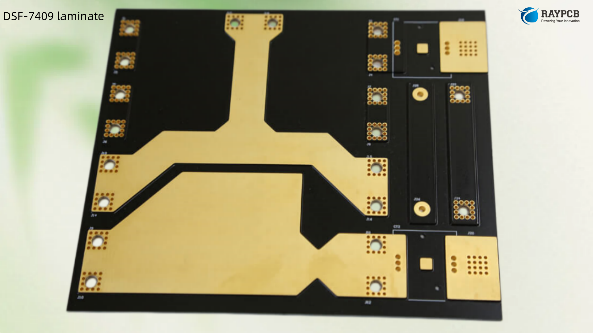
The DS-7409HF is a high-Tg, halogen-free, FR-4-class copper-clad laminate (CCL) produced by Doosan PCB Electro-Materials, a South Korean specialty chemicals and electronic materials company. It belongs to Doosan’s DS-7400 series, which is engineered specifically to meet modern environmental and thermal reliability requirements.

Unlike standard FR-4, which uses brominated flame retardants (BFRs) to meet UL 94 V-0, the DS-7409HF uses phosphorus-based and nitrogen-based flame retardant chemistry โ€” no chlorine, no bromine above trace levels. This makes it genuinely halogen-free per IEC 61249-2-21, not just “low-halogen.”

For PCB engineers, this distinction matters. Many materials labeled “halogen-free” are simply low-halogen. IEC 61249-2-21 sets specific thresholds:

HalogenIEC 61249-2-21 Limit
Chlorine (Cl)โ‰ค 900 ppm
Bromine (Br)โ‰ค 900 ppm
Total halogensโ‰ค 1500 ppm

DS-7409HF meets all three thresholds comfortably.

DS-7409HF Key Technical Specifications

Here’s a quick-reference table for the most critical parameters engineers pull when qualifying a laminate:

PropertyTest MethodTypical Value
Glass Transition Temperature (Tg)DSC (IPC-TM-650 2.4.25)150ยฐC
Decomposition Temperature (Td)TGA (5% weight loss)โ‰ฅ 340ยฐC
T-288 (time-to-delamination)IPC-TM-650 2.4.24.1> 10 min
CTE (Z-axis, 50โ€“260ยฐC)TMAโ‰ค 3.5%
CTI (Comparative Tracking Index)IEC 60112โ‰ฅ 600 V (Group I)
Dielectric Constant (Dk) @ 1 GHzIPC-TM-650 2.5.5.9~4.5
Dissipation Factor (Df) @ 1 GHzIPC-TM-650 2.5.5.9~0.015
Flexural Strength (lengthwise)IPC-TM-650 2.4.4โ‰ฅ 415 MPa
Water AbsorptionIPC-TM-650 2.6.2โ‰ค 0.15%
FlammabilityUL 94V-0
RoHS ComplianceEU Directive 2011/65/EUYes

The T-288 value is probably the most practically useful number on that table. It tells you how long the laminate can survive at 288ยฐC (typical lead-free solder pot temperature) before delamination begins. Anything above 10 minutes is solid for lead-free assembly. DS-7409HF clears that comfortably.

RoHS Compliance: What It Actually Means for DS-7409HF

RoHS (Restriction of Hazardous Substances, EU Directive 2011/65/EU, updated by 2015/863/EU) restricts ten substances in electrical and electronic equipment. For laminate materials, the most relevant restrictions are:

  • Lead (Pb):ย โ‰ค 0.1% by weight in homogeneous materials
  • Cadmium (Cd):ย โ‰ค 0.01%
  • Hexavalent chromium (Cr VI):ย โ‰ค 0.1%
  • Polybrominated biphenyls (PBB):ย โ‰ค 0.1%
  • Polybrominated diphenyl ethers (PBDE):ย โ‰ค 0.1%

DS-7409HF satisfies all ten RoHS restricted substance limits. Since it contains no brominated flame retardants at all, PBB and PBDE concerns are eliminated at the chemistry level โ€” not just managed to stay under threshold.

This is an important point for product compliance documentation. When your customer asks for a full material declaration (FMD) or an IPC-1752A Class D declaration, having a material with zero brominated content is much cleaner to document than one that’s simply “under limit.”

REACH and SCIP Considerations

Beyond RoHS, the EU REACH regulation (SVHC substances of very high concern) and the SCIP database requirements increasingly affect PCB laminate sourcing. Doosan provides REACH compliance documentation for DS-7409HF, confirming no SVHC substances above 0.1% threshold.

Why PCB Engineers Choose DS-7409HF Halogen-Free Over Standard FR-4

Thermal Performance at Lead-Free Assembly Temperatures

The industry shift to lead-free soldering (SAC305 alloy, peak reflow at ~260ยฐC) put a lot of pressure on laminates that were designed for eutectic tin-lead (peak ~183ยฐC). Standard FR-4 with Tg of 130ยฐC struggles. DS-7409HF’s 150ยฐC Tg and โ‰ฅ340ยฐC Td give you meaningful margin above lead-free reflow peaks, especially important for thick multilayer boards with many reflow cycles.

Moisture Absorption and Long-Term Reliability

Water absorption directly affects signal integrity at high frequencies and dimensional stability. At โ‰ค 0.15%, DS-7409HF is notably better than many standard halogen-free alternatives which can creep toward 0.2โ€“0.3%. For outdoor telecom enclosures, industrial control boards, or automotive ADAS modules, this matters.

CTI โ‰ฅ 600V โ€” Practical Impact

CTI (Comparative Tracking Index) of Group I (โ‰ฅ 600V) isn’t just a spec box to check โ€” it directly affects your PCB creepage and clearance calculations under IEC 60664-1. A higher CTI material allows smaller creepage distances for a given voltage level, which can meaningfully reduce board area on high-voltage industrial or EV charging designs.

DS-7409HF vs. Competing Halogen-Free Laminates

How does it stack up against other commonly specified halogen-free materials?

MaterialManufacturerTg (ยฐC)Td (ยฐC)CTIDk @ 1GHzNotable Use Case
DS-7409HFDoosan150โ‰ฅ 340โ‰ฅ 600 V~4.5Industrial, Automotive
IT-158Iteq150360โ‰ฅ 600 V~4.6Telecom, Server
S1000-2MSytech170340โ‰ฅ 600 V~4.8High-layer Multilayer
TU-768TUC175360โ‰ฅ 600 V~4.6High-Reliability Industrial
Megtron 6Panasonic185400โ‰ฅ 600 V~3.7High-Speed Digital, RF

DS-7409HF sits in the sweet spot for cost-performance balance โ€” better thermal performance than entry-level halogen-free FR-4 derivatives, without the price premium of high-speed laminates like Megtron 6 (which you probably don’t need unless your signals are running above 10 Gbps).

Typical Applications for DS-7409HF Halogen-Free Laminate

Based on its property profile, DS-7409HF is well-suited for:

  • Industrial control boardsย โ€” motor drives, PLCs, power converters
  • Automotive electronicsย โ€” body control modules (BCM), ADAS sensor interfaces (not cutting-edge radar, but tier-2 functional boards)
  • Telecommunications infrastructureย โ€” access network equipment, switches, routers
  • Medical equipment PCBsย โ€” where halogen-free is increasingly a procurement requirement
  • LED lighting driversย โ€” high-temperature ambient environments
  • Power supply PCBsย โ€” where CTI Group I provides design flexibility

It’s generally not the right call for high-frequency RF boards above ~6 GHz (Dk/Df isn’t optimized for that), or extreme thermal cycling automotive applications (dedicated automotive-grade materials are better there).

Processing Guidelines for DS-7409HF

A few practical notes for your fab and assembly teams:

Drilling: Halogen-free laminates tend to be slightly more brittle than standard FR-4 due to the different resin chemistry. Use fresh drill bits, and reduce feed rate by ~10% compared to your standard FR-4 baseline to avoid drill smear.

Desmear: The higher cross-link density in halogen-free resins means desmear needs to be slightly more aggressive. Confirm with your fab house that their permanganate desmear cycle is calibrated for HF materials โ€” not all fab lines default to this.

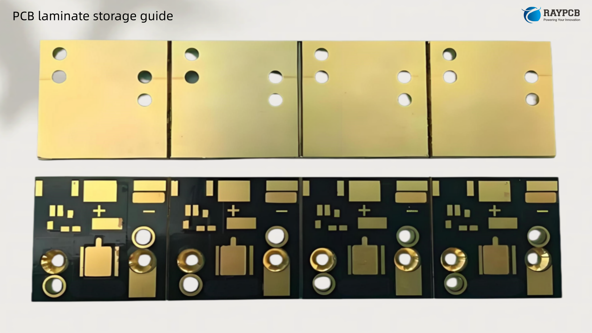
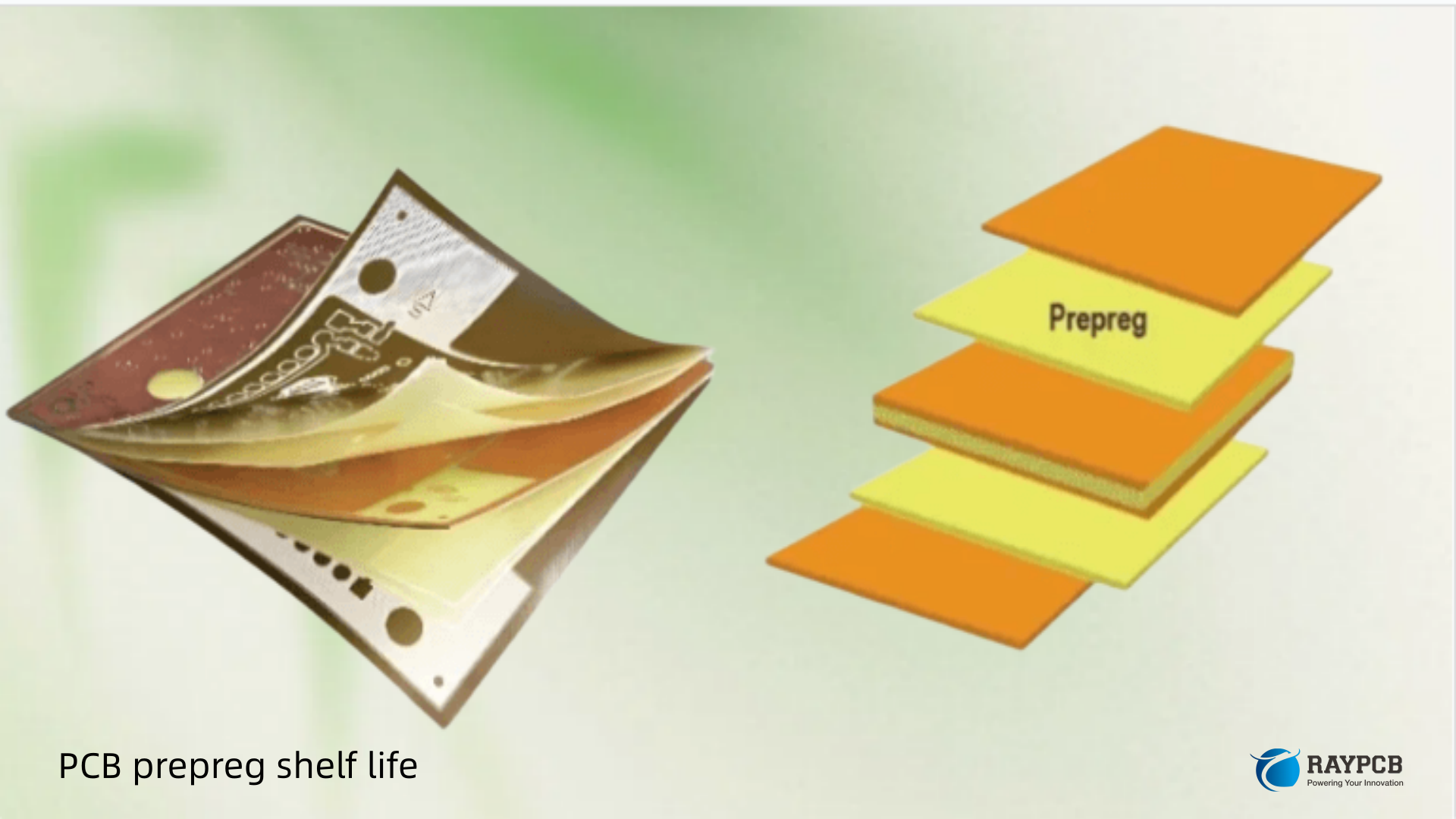
Storage: Keep panels in sealed moisture barrier bags with desiccant at 20โ€“30ยฐC, below 60% RH. Pre-bake at 120ยฐC for 2โ€“4 hours before lamination if panels have been exposed beyond manufacturer’s shelf-life window.

Lead-Free Reflow: Compatible with SAC305. Typical peak reflow at 245โ€“260ยฐC. The T-288 margin of >10 minutes covers multiple reflow cycles without issue.

Useful Resources for DS-7409HF Halogen-Free Laminate

ResourceDescriptionLink
IPC-4101Base Materials for Rigid and Multilayer PCBs (laminate spec standard)ipc.org
IEC 61249-2-21Halogen-free definition and test methodologyiec.ch
EU RoHS Directive 2011/65/EUFull restricted substance listec.europa.eu
IPC-TM-650Test Methods Manual (laminate property testing)ipc.org/TM-650
Doosan PCB Materials PageDoosan laminate product rangeDoosan PCB
ECHA SCIP DatabaseEU SCIP substance-of-concern notificationsecha.europa.eu
UL Product iQUL flammability certifications lookupiq.ul.com

5 FAQs About DS-7409HF Halogen-Free Laminate

Q1: Is DS-7409HF truly halogen-free or just “low-halogen”? It is genuinely halogen-free per IEC 61249-2-21, meaning Cl โ‰ค 900 ppm, Br โ‰ค 900 ppm, and total halogens โ‰ค 1500 ppm. Doosan achieves this through phosphorus/nitrogen-based flame retardants with no brominated compounds in the resin system.

Q2: Can I use DS-7409HF in an automotive application? For most automotive body electronics and functional modules (BCM, lighting, HVAC control), yes. For powertrain, advanced ADAS, or AEC-Q200-qualified components requiring AEC-qualified laminate, you’d want to verify with Doosan on specific automotive qualification status before committing.

Q3: How does the Dk of ~4.5 affect high-speed signal integrity? At 1โ€“3 GHz, it’s perfectly adequate for DDR4/DDR5 interfaces and standard Ethernet up to 10GbE with proper stackup design. Above ~6โ€“8 GHz or for PCIe Gen 5 with tight channel budgets, consider a lower-Dk/Df material.

Q4: Does DS-7409HF require any special storage conditions compared to standard FR-4? Yes, slightly. Halogen-free resins can be more hygroscopic than brominated alternatives. Maintain storage below 60% RH, and pre-bake panels if they’ve been in ambient conditions for more than a week. Check Doosan’s published shelf-life data for your specific thickness/copper weight combination.

Q5: Is DS-7409HF compatible with OSP, ENIG, and HASL finishes? Yes to all three. It is also compatible with ENEPIG and immersion tin. For lead-free HASL, ensure the solder pot temperature profile is controlled tightly โ€” the laminate handles it fine at recommended dwell times, but extended exposure above 265ยฐC should be avoided.

Final Thoughts

The DS-7409HF halogen-free laminate hits a useful middle ground that a lot of designs actually need: solid thermal performance for lead-free assembly, clean RoHS and IEC 61249-2-21 compliance without greenwashing, CTI Group I for high-voltage designs, and a reasonable cost delta over standard FR-4. It’s not exotic, but that’s often exactly the point. For industrial, telecom, and mid-range automotive PCBs, specifying DS-7409HF means your compliance documentation is clean, your fab process is predictable, and you’re not over-paying for performance you don’t need.

If you’re qualifying it for a new design, get the current datasheet direct from Doosan Electro-Materials, cross-reference against IPC-4101 slash sheet requirements for your stackup, and confirm your fab house’s experience with HF materials before committing to production panelization.

DSF-7409 Review: Enhanced Thermal FR-4 for Industrial PCBs

A technical review of DSF-7409 laminate from Doosan โ€” the enhanced thermal FR-4 built for industrial PCBs. Covers key specs (Tg โ‰ฅ170ยฐC, T-260 >60 min), comparison vs. standard FR-4, fabrication tips, application fit, and 5 engineering FAQs.

There’s a specific kind of frustration that comes from picking a laminate that looks fine on paper โ€” decent Tg, standard FR-4 pricing, familiar process window โ€” and then watching it fail after three lead-free reflow passes on an industrial motor drive board. That’s the situation that drives engineers toward enhanced-thermal FR-4 variants. The DSF-7409 laminate sits squarely in that conversation: it’s a multifunctional epoxy-based copper-clad laminate (CCL) from Doosan Electro-Materials, built on the well-established DS-7409 platform but tuned for environments where standard FR-4 runs out of headroom.

If you’re specifying material for PLC backplanes, power conversion boards, or any industrial electronics that will see wide thermal cycling and multiple solder reflow events, this material is worth a close look.

What Is DSF-7409 Laminate?

DSF-7409 is part of the broader Doosan PCB material family, which has been developed by Doosan Electro-Materials โ€” a Korean manufacturer founded in 1974 that has grown into one of the significant CCL producers in the Asia-Pacific market. The DSF-7409 designation refers to a multifunctional epoxy resin-based laminate with an elevated glass transition temperature, enhanced chemical resistance, and compatibility with modern lead-free assembly processes.

The “multifunctional epoxy” descriptor is important. Standard FR-4 typically uses difunctional or bifunctional bisphenol-A epoxy resins, which cure into a relatively loosely cross-linked polymer network. Multifunctional epoxy systems add additional reactive sites, producing a denser cross-linked structure after cure. That denser network is what pushes the Tg up and improves resistance to thermal decomposition โ€” both of which matter enormously in industrial PCB applications.

Key Technical Specifications of DSF-7409 Laminate

Understanding what you’re working with starts at the datasheet. Below is a summary of the core property profile for DSF-7409 laminate:

PropertyTest MethodTypical Value
Glass Transition Temperature (Tg)DSC โ€“ IPC-TM-650 2.4.25โ‰ฅ 170ยฐC
Thermal Decomposition Temp (Td)TGA โ€“ IPC-TM-650 2.4.40โ‰ฅ 320ยฐC
T-260 (Time to Delamination)TMA โ€“ IPC-TM-650 2.4.24.1> 60 min
Z-axis CTE (50โ€“260ยฐC)TMAโ‰ค 3.5%
Dielectric Constant (Dk) at 1 GHzIPC-TM-650 2.5.5~4.2
Dissipation Factor (Df) at 1 GHzIPC-TM-650 2.5.5~0.015
Peel Strength (1 oz Cu, Condition A)IPC-TM-650 2.4.8โ‰ฅ 2.0 N/mm
Water AbsorptionIPC-TM-650 2.6.2โ‰ค 0.13%
FlammabilityUL 94V-0
UL Recognitionโ€”E103670
BSI Certificationโ€”6741
UV Blocking / AOI Compatibleโ€”Yes

The T-260 result โ€” exceeding 60 minutes โ€” is a standout number for industrial applications. It means the laminate can hold up to extended thermal soak at 260ยฐC without delaminating, which gives fabricators meaningful margin when boards go through rework or extended reflow profiles.

Why Industrial PCBs Demand More Than Standard FR-4

In a typical consumer electronics design, a board might see two reflow passes and then live on a shelf in a temperature-controlled room. Industrial electronics are not so forgiving. A variable frequency drive board in a factory cabinet might see ambient swings from -20ยฐC to 85ยฐC daily. A motor controller running at high duty cycles can have localized component temperatures that stress the substrate continuously. Add lead-free solder assembly with peak temperatures north of 250ยฐC, and you’re asking a lot of your laminate.

Here’s where standard FR-4 tends to fall short in industrial contexts:

Thermal excursion degradation โ€” When the substrate repeatedly cycles through temperatures near or above its Tg, the resin micro-structure gradually degrades. You may not see visible delamination on the first pass, but z-axis barrel fatigue on plated through-holes accumulates over time.

Moisture sensitivity in harsh environments โ€” Industrial boards sometimes live in humid or chemically aggressive environments. A laminate with poor moisture resistance will absorb humidity, which drives ion migration and can compromise insulation resistance over months or years of service.

CAF (Conductive Anodic Filament) growth โ€” Fine-pitch industrial boards with high-density via patterns are vulnerable to CAF between adjacent conductors, especially when exposed to moisture and DC bias voltage over long service lives. A tighter, denser resin matrix resists filament growth more effectively.

DSF-7409 laminate was developed to address each of these failure modes with a coherent material solution rather than a patchwork of workarounds.

DSF-7409 vs. Standard FR-4: The Engineering Gap

Let’s put some numbers to the comparison so the upgrade decision has a concrete basis:

ParameterStandard FR-4 (Tg ~135ยฐC)DSF-7409 Laminate
Tg (DSC)130โ€“140ยฐCโ‰ฅ 170ยฐC
Td~300ยฐCโ‰ฅ 320ยฐC
T-2605โ€“15 min> 60 min
Z-axis CTE (50โ€“260ยฐC)~4.0โ€“4.5%โ‰ค 3.5%
Lead-Free Reflow CompatibilityMarginalFully compatible
UV Blocking / AOI CompatibilityNot alwaysYes
Halogen Compliance OptionsStandard halogenatedAvailable
Cost Premium Over Standard FR-4Baseline~10โ€“20%

The CTE improvement matters more than most engineers initially expect. Every 0.5% reduction in z-axis expansion translates to meaningfully lower barrel stress on through-hole copper during thermal cycling. For boards with via densities above 8 vias/cmยฒ, this improvement extends the service life measurably.

Core Features That Set DSF-7409 Laminate Apart

Multifunctional Epoxy Resin System

The resin system is the heart of the material. DSF-7409’s multifunctional epoxy delivers more reactive cross-linking sites per molecule than conventional bisphenol-A systems. The practical result is a polymer network that holds together better at elevated temperatures, resists moisture uptake more effectively, and is less prone to micro-cracking under thermal cycling stress.

UV Blocking and AOI Compatibility

This one often gets overlooked, but it’s genuinely useful in a production context. The UV blocking characteristic means the laminate appears opaque to automated optical inspection (AOI) systems, which dramatically reduces false positives on board defect inspection lines. For high-mix industrial assembly where AOI is a critical quality gate, this feature saves real time.

Excellent Chemical Resistance

Industrial boards sometimes get exposed to cleaning solvents, flux residues, and process chemicals during assembly and in service. The multifunctional resin system provides better resistance to chemical attack compared to standard FR-4, preserving electrical insulation properties over the product’s service life.

Good Performance Through Multiple Thermal Excursions

The phrase “multiple thermal excursions” in Doosan’s material documentation refers specifically to the ability to withstand repeated lead-free reflow cycles without delamination, measling, or crazing. For double-sided SMT assembly with rework cycles, this is a hard requirement rather than a nice-to-have.

Industrial Application Fit for DSF-7409 Laminate

ApplicationWhy DSF-7409 Makes Sense
PLC and DCS Control BoardsWide temp cycling, long service life, moisture exposure
Variable Frequency Drives (VFDs)High thermal dissipation, multiple reflow cycles
Power Supply Boards (industrial)Sustained thermal stress, lead-free assembly
Motor ControllersVibration plus thermal, need stable CTE
Test & Measurement EquipmentReliability critical, often Class 3 IPC spec
Telecommunications InfrastructureMulti-layer boards with fine-pitch BGAs
Military and Defense ElectronicsIPC Class 3, demanding reliability specs

One point worth making to procurement teams: the 10โ€“20% cost premium on DSF-7409 over commodity FR-4 is recovered many times over if it prevents a single field failure on an industrial board. Industrial electronics typically have long service life expectations (10โ€“20 years for a PLC isn’t unusual), and the reliability math strongly favors the upgraded material.

Fabrication Notes for DSF-7409 Laminate

Working with DSF-7409 is not dramatically different from standard FR-4, but a few process parameters deserve attention before you run your first panel.

Press Lamination

Multifunctional epoxy systems typically require slightly more aggressive cure conditions compared to standard bifunctional FR-4. Check Doosan’s processing guide for recommended press temperature, pressure, and dwell time. Using a standard FR-4 lamination cycle may result in under-cure, which will degrade both Tg performance and chemical resistance in the finished board.

Drilling

Higher-Tg materials tend to be marginally more abrasive on carbide drill bits due to the denser resin matrix. Monitor bit usage more closely on multilayer stackups and consider adjusting feed rates on thicker cores. Hole wall quality is critical for barrel reliability in industrial applications โ€” don’t let bit wear compromise it.

Plasma Desmear

Dense resin systems are less reactive to desmear chemistry. Verify that your plasma etch process is achieving clean etchback on inner-layer copper and through-hole walls before plating. Running qualification coupons when transitioning from standard FR-4 to DSF-7409 is worth the time investment.

Pre-Assembly Bake

Even with DSF-7409’s low water absorption (โ‰ค 0.13%), pre-baking assembled boards at 120ยฐC for 2โ€“4 hours before lead-free reflow is standard good practice, especially for boards stored in warehouses or shipped through humid transit conditions.

DSF-7409 Compared to Competing Enhanced-Thermal FR-4 Materials

MaterialManufacturerTg (DSC)Lead-Free CompatibleNotable Use Case
DSF-7409Doosanโ‰ฅ 170ยฐCYesIndustrial, mil, telecom
370HRIsolaโ‰ฅ 180ยฐCYesStrong North America presence
TU-768TUCโ‰ฅ 170ยฐCYesPopular in Taiwan fabs
IT-180AIteqโ‰ฅ 175ยฐCYesCost-competitive alternative
S1000-2Shengyiโ‰ฅ 170ยฐCYesHigh-volume Chinese fabricators

DSF-7409 is well-positioned in the mainstream high-reliability segment. It competes on performance with 370HR and IT-180A while offering the sourcing reliability of an established Korean manufacturer with a long track record in the CCL market.

Useful Resources for Engineers and Procurement

  • Doosan Electro-Materials Product Pagesย โ€” Full datasheets, RoHS documentation, and MSDS downloads for all DS/DSF-7409 variants: https://www.doosanelectromaterials.com
  • IPC-4101E โ€“ Specification for Base Materials for Rigid and Multilayer Printed Boardsย โ€” The key industry document for laminate classification and qualification: https://www.ipc.org
  • IPC-TM-650 Test Methods Manualย โ€” Defines T-260, T-288, CTE, peel strength, and all other standard laminate test procedures: https://www.ipc.org/TM
  • IPC-6012ย โ€” Qualification and Performance Specification for Rigid PCBs, including Class 3 industrial requirements: https://www.ipc.org
  • UL Product iQ Databaseย โ€” Verify UL recognition status (E103670) for Doosan materials directly: https://iq.ul.com
  • IEC 61249-2-21ย โ€” International standard for halogen-free base materials, relevant if your industrial design requires halogen-free compliance

Frequently Asked Questions About DSF-7409 Laminate

Q1: Is DSF-7409 laminate halogen-free?

The base DS-7409 / DSF-7409 platform is available in both standard and halogen-free variants depending on the specific grade suffix. If halogen-free compliance is a project requirement โ€” common in European industrial markets under IEC 61249-2-21 โ€” confirm the specific part number includes halogen-free certification before ordering material. When writing fab notes, specify “halogen-free per IEC 61249-2-21” explicitly to avoid substitution risk.

Q2: How many lead-free reflow cycles can DSF-7409 reliably withstand?

Based on the T-260 performance (>60 min) and the multifunctional resin system, DSF-7409 is well-suited for 6 or more simulated reflow passes without structural failure. In practical production, that covers double-sided SMT assembly, selective soldering, and 1โ€“2 rework cycles with margin to spare. Actual results depend on your specific press lamination quality and reflow profile.

Q3: Can DSF-7409 laminate be processed on the same equipment as standard FR-4?

Yes, the same drill, router, plating, and lamination equipment applies. The key differences are in process parameter settings, particularly lamination cure profile and plasma desmear chemistry/duration. Don’t assume identical parameters โ€” qualify DSF-7409 through a coupon run before committing full production panels. The one-time qualification effort is much less costly than a delamination problem in production.

Q4: What IPC-4101E slash sheet does DSF-7409 map to?

DSF-7409 with Tg โ‰ฅ 170ยฐC and multifunctional epoxy resin maps to IPC-4101E /126 (high-performance FR-4, Tg โ‰ฅ 150ยฐC by TMA, multifunctional epoxy) when referencing standard classification. Confirm the specific slash sheet with Doosan’s technical documentation or your fab house’s qualified materials list before writing final procurement specs.

Q5: What is the typical availability and lead time for DSF-7409 laminate?

Doosan materials are stocked by CCL distributors across Asia, Europe, and North America. For standard panel sizes and core thicknesses (0.2mm to 3.2mm), inventory is generally available. Custom configurations or specific prepreg combinations may involve 4โ€“8 week lead times depending on the distributor. When managing a design transition from standard FR-4, build a buffer into your first production run schedule to accommodate any material sourcing variation.

The Bottom Line

DSF-7409 laminate occupies a pragmatic middle ground โ€” it’s not an exotic low-loss RF material, and it’s not priced like one. What it is, is a well-engineered, industrially validated enhanced-thermal FR-4 that solves real-world failure modes in demanding PCB applications. The combination of Tg โ‰ฅ 170ยฐC, T-260 > 60 minutes, UV-blocking capability, lead-free process compatibility, and Doosan’s manufacturing consistency makes it a sensible default choice any time standard FR-4’s thermal headroom is genuinely insufficient.

For industrial electronics engineers, the real question isn’t whether DSF-7409 is worth the modest cost premium. The question is whether the application can afford the risk of using something less capable.

Suggested Meta Description:

A technical review of DSF-7409 laminate from Doosan โ€” the enhanced thermal FR-4 built for industrial PCBs. Covers key specs (Tg โ‰ฅ170ยฐC, T-260 >60 min), comparison vs. standard FR-4, fabrication tips, application fit, and 5 engineering FAQs.

Is Doosan PCB Material RoHS Compliant? A PCB Engineer’s Complete Guide

Doosan PCB RoHS compliance guide: which products are halogen-free, what certificates to download, REACH status, and how to build your compliance document trail.

If you’re specifying a laminate supplier for a product that ships into Europe, you already know the first question procurement is going to ask: “Is this material RoHS compliant?” For engineers working with Doosan copper clad laminates, the short answer is yes โ€” but the full picture is worth understanding before you sign off on a BOM or write your compliance documentation.

This guide covers Doosan PCB RoHS compliance from the ground up: what the directive actually requires, how Doosan’s product lines meet those requirements, what halogen-free means in practice, and what documentation your fabricator and compliance team will expect you to produce.

What RoHS Compliance Actually Means for PCB Laminate

RoHS stands for “Restriction of Hazardous Substances” and originated as a European Union directive known as Directive 2002/95/EC, adopted in February 2003. The motivation was to address health and environmental concerns around substances like lead, mercury, cadmium, and other heavy metals found in electronics.

The current version, RoHS 3 (Directive 2015/863), added four more phthalates โ€” BBP, DBP, DEHP, and DIBP โ€” to the original restricted substances list. That gives us ten total restricted substances that any PCB laminate destined for EU-market products must address.

The maximum permitted concentrations in non-exempt products are 0.1% or 1000 ppm (except for cadmium, which is limited to 0.01% or 100 ppm) by weight in each homogeneous material.

For a laminate manufacturer like Doosan, this means the resin system, glass reinforcement, copper foil, and any surface treatments must all independently meet these thresholds. It’s not a board-level average โ€” it’s material by material.

Doosan PCB RoHS Compliance: The Direct Answer

Doosan products comply with RoHS directive requirements and REACH regulation. Their halogen-free product lines meet IEC 61249-2-21 requirements with bromine content below 900 ppm and chlorine below 900 ppm.

Every current Doosan CCL product page on the Doosan Electro-Materials website includes a downloadable RoHS certificate and MSDS sheet as standard. Whether you’re looking at the DS-7409 series for high-speed digital, the DS-7409HG family for IC substrate applications, or the ILD PTFE-based series for mmWave RF, RoHS documentation is available at the product level.

What’s worth noting is that Doosan doesn’t treat RoHS compliance as a single checkbox. Their product lineup is structured into two environmental tiers that engineers should understand clearly.

Tier 1: RoHS-Compliant (Standard Halogenated)

This covers products that meet all ten RoHS restricted substance limits, including limits on specific brominated flame retardants like PBB and PBDE. However, these products may still use TBBPA (tetrabromobisphenol A) as a flame retardant โ€” currently still permitted under RoHS, though regulators were expected to add TBBPA to the restricted substances list as of 2023, though this has been delayed as of mid-2024. Engineers specifying these materials for long product lifecycles should flag this as a watch item.

Tier 2: RoHS-Compliant + Halogen-Free

This is where Doosan’s “HG” suffix products sit. The DS-7409HG series is halogen, antimony, and red phosphorus free, and is designed for IC package substrate applications including NAND Flash memory. The halogen-free designation goes beyond basic RoHS โ€” it eliminates chlorine and bromine flame chemistry entirely, replacing it with phosphorus-nitrogen or inorganic alternatives.

A halogen-free PCB is defined by IEC 61249-2-21 as having bromine and chlorine content each below 900 ppm, with total halogens under 1500 ppm. This applies to the entire board, including laminate, prepreg, and solder mask.

Doosan Product Lines and Their Compliance Status

Product SeriesApplicationHalogen-FreeRoHS Cert AvailableKey Feature
DS-7409DVNetwork switches, serversNo (RoHS โœ“)YesLow-loss, standard HF-free
DS-7409DV(N)400G routers, computingNo (RoHS โœ“)YesUltra-low loss
DS-7409DQN800G backplane, 5G base stationYes (HF + RoHS โœ“)YesSuper ultra-low loss, halogen-free
DS-7409HG(I)IC Package โ€“ NAND FlashYes (HF + RoHS โœ“)YesLow CTE, High Tg
DS-7409HG(ZL)IC Package โ€“ Mobile DRAMYes (HF + RoHS โœ“)YesHigh modulus
DS-7409HG(KN)IC Package โ€“ 5G AiPYes (HF + RoHS โœ“)YesLow Dk/Df
DS-7409HG(IQ)FC BGA โ€“ Non-MemoryYes (HF + RoHS โœ“)YesMechanical drill compatible
ILD SeriesmmWave, automotive radar, 5G/6GYes (HF + RoHS โœ“)YesPTFE-based ultra-low loss

For engineers designing Doosan PCB material into a new product, the table above maps compliance tier directly to application, which is exactly how a fabricator or compliance auditor will want to see it structured.

RoHS vs. Halogen-Free: Why the Distinction Matters in Practice

This is a point that trips up a lot of engineers at the BOM review stage. RoHS compliance and halogen-free status are related but not identical.

RoHS directives prohibit the use of specific types of brominated flame retardants โ€” PBB and PBDE specifically โ€” but not all brominated compounds are restricted. TBBPA, the most common flame retardant in standard FR-4, is still permitted under current RoHS rules. A product can be 100% RoHS compliant while still containing bromine.

Halogen-free materials go further: they eliminate bromine and chlorine from the entire formulation. In fire scenarios, halogen-free boards produce far less toxic smoke and corrosive gases โ€” independent tests show smoke density reduced by 50โ€“70% compared to halogenated materials. For data centers, aerospace, rail, and medical applications, this performance difference is often a contractual or safety-standard requirement, not just a regulatory one.

What Documentation Doosan PCB RoHS Compliance Requires

All materials used for a PCB must be traceable to meet regulatory requirements. Documentation during manufacturing is crucial to establish records that all materials are RoHS compliant and have not been liable to cross-contamination.

For a Doosan-based design, your compliance package should include:

DocumentSourcePurpose
Doosan RoHS CertificateDoosan product page downloadDeclares per-product restricted substance limits
MSDS (Material Safety Data Sheet)Doosan product page downloadSubstance declaration for procurement audit
IEC 61249-2-21 Compliance StatementDoosan (for HG series)Halogen-free verification
Fabricator’s RoHS Process DeclarationYour PCB manufacturerConfirms lead-free assembly compatibility
Surface Finish SpecificationFabrication noteMust specify ENIG, ENEPIG, or immersion tin/silver

RoHS-compliant surface finishes include immersion silver, immersion tin, or ENIG (Electroless Nickel Immersion Gold) โ€” these replace finishes containing restricted substances like lead or cadmium.

Useful Compliance Resources for PCB Engineers

These resources are essential references when preparing documentation or specifying Doosan materials for regulated markets:

  • Doosan Electro-Materials CCL Product Portalย โ€” doosanelectromaterials.comย โ€” Per-product RoHS and MSDS downloads
  • EU RoHS Official Directive Text (2011/65/EU and 2015/863)ย โ€” eur-lex.europa.euย โ€” Primary legislative source for RoHS 2 and RoHS 3
  • IEC 61249-2-21 Standardย โ€” iec.chย โ€” Halogen-free laminate material specification
  • IPC-1752A Material Declaration Standardย โ€” ipc.orgย โ€” Industry-standard format for substance declaration forms
  • ECHA REACH SVHC Candidate Listย โ€” echa.europa.euย โ€” Updated list of Substances of Very High Concern under REACH
  • IEC 63000:2016ย โ€” iec.chย โ€” Technical documentation standard for RoHS assessment of EEE

5 FAQs on Doosan PCB RoHS Compliance

Q1. Does every Doosan laminate product come with a downloadable RoHS certificate?

Yes. Every current CCL product on the Doosan Electro-Materials website includes a dedicated “RoHS Download” button alongside the MSDS download. These are product-specific declarations, not blanket company-level statements โ€” which is what your quality team and auditors will want.

Q2. Is the DS-7409DQN halogen-free and RoHS compliant at the same time?

Yes. The DS-7409DQN is explicitly listed as halogen-free and is positioned for 800G network equipment and 5G/6G base station applications, with both an RoHS download and MSDS available on the product page. This makes it one of Doosan’s most fully compliant high-speed options for regulated-market designs.

Q3. Will TBBPA eventually become a restricted substance under RoHS?

It’s a genuine watch item. The EU was expected to restrict TBBPA under RoHS 3 as of 2023, but the proposal was delayed as of July 2024. If you’re designing a product with a 5โ€“10 year lifecycle, specifying a halogen-free Doosan product now โ€” like the HG or DQN series โ€” insulates your design against that future regulatory move.

Q4. Does RoHS compliance guarantee the laminate is also REACH compliant?

Not automatically โ€” they are separate regulatory frameworks. Doosan products comply with both RoHS directive requirements and REACH regulation, with environmental declarations and conflict minerals documentation available through Doosan’s quality department. Confirm REACH compliance separately and request the SVHC declaration alongside your RoHS certificate.

Q5. Do Doosan halogen-free laminates process the same as standard FR-4 on the fab floor?

In most cases, yes. The DS-7409HG series is described as compatible with similar FR-4 PCB processing, which means your fabricator typically does not need new press cycles, drill parameters, or chemistry for standard multilayer builds. Higher-performance variants may require specific lamination profiles โ€” always confirm with your fabricator before committing to a stack-up.

The Bottom Line on Doosan PCB RoHS Compliance

Doosan’s laminate portfolio is fully RoHS compliant across its entire product lineup. For engineers who need to go further โ€” halogen-free, REACH-compliant, or prepared for future TBBPA restrictions โ€” the HG and DQN product families deliver all of that without forcing a change in fabrication process or a significant cost penalty.

The documentation infrastructure is there: per-product RoHS certificates, MSDS sheets, and IEC 61249-2-21 compliance declarations are all downloadable directly from the Doosan product portal. That makes the compliance audit trail straightforward to build, which is exactly what you need when your product goes to CE marking review or a tier-one OEM qualification.

Know your tier. Get your documents. And make sure your fabricator’s process declaration aligns with the laminate you specified.

Suggested Meta Descriptions

Option A (Direct answer, keyword-first, 155 chars):

“Doosan PCB RoHS compliance explained: full product-by-product breakdown, halogen-free vs RoHS differences, required documentation, and FAQs for engineers.”

Option B (Question-led, 153 chars):

“Is Doosan PCB material RoHS compliant? Yes โ€” here’s the full engineer’s guide to DS-7409 and HG series compliance, documentation, and halogen-free status.”

Option C (Benefit-focused, 157 chars):

“Doosan PCB RoHS compliance guide: which products are halogen-free, what certificates to download, REACH status, and how to build your compliance document trail.”

Recommended: Option B โ€” it directly mirrors the search query (“Is Doosan PCB material RoHS compliant?”), answers it immediately with “Yes,” and signals depth of content (engineer’s guide, DS-7409, HG series, halogen-free) โ€” all within the 160-character Yoast limit.

ILD-0.3 Low-Loss PCB Material: Dk 3.0 for High-Frequency Design

ILD-0.3 PCB material specs, Dk 3.0 dielectric properties, Df performance, applications in 5G antennas, ADAS radar & high-speed digital design. Full technical guide with tables, comparisons & 5 FAQs.

When the dielectric constant of your substrate starts mattering more than the trace routing, you’re working in the territory where material selection is the design. ILD-0.3 PCB material sits squarely in that territory โ€” a low-loss laminate with a dielectric constant of 3.0, engineered for the class of high-frequency applications where standard FR-4’s Dk of 4.2โ€“4.7 and dissipation factor above 0.015 simply cannot deliver the signal fidelity the circuit demands.

This article covers what ILD-0.3 PCB material is, what its Dk 3.0 / low-loss profile means in practical RF and high-speed digital design terms, how it compares against competing materials in the same class, and where it belongs in your stackup. If you’re evaluating it against alternatives โ€” or you’ve landed on this page because someone in your supply chain specified it and you need to understand what you’re dealing with โ€” this is the reference you need.

What Is ILD-0.3 PCB Material and Why Dk 3.0 Matters

ILD-0.3 is a low-loss dielectric laminate material with a nominal dielectric constant (Dk) of 3.0. That Dk figure puts it at the boundary between mid-range and advanced-class high-frequency materials โ€” lower than the modified epoxy/hydrocarbon materials in the 3.3โ€“3.7 range (like Rogers RO4350B at 3.48, or Isola FR408HR at 3.68), and comparable to specialized antenna-grade laminates like Rogers RO4730G3, which also targets Dk 3.0 for antenna array applications.

The significance of Dk 3.0 isn’t abstract. Signal propagation velocity through a PCB trace is inversely proportional to the square root of Dk. Put another way: a material with Dk 3.0 allows signal propagation that is approximately 18% faster than the same trace built on standard FR-4 (Dk 4.5). For a 100mm microstrip line at 10 GHz, that translates directly to a measurable difference in phase delay, impedance stability, and insertion loss โ€” the three numbers that determine whether your RF design hits spec or misses it.

The “low-loss” designation refers to the dissipation factor (Df, also called loss tangent), which governs how much signal energy is converted to heat per unit length of trace. For ILD-0.3 PCB material in the Dk 3.0 class, the typical Df target is below 0.003 at 10 GHz, which is roughly 5โ€“7x lower than standard FR-4. At frequencies above 5 GHz, this difference dominates insertion loss calculations. A trace on FR-4 that loses 3 dB per 100mm at 10 GHz will lose under 1 dB on ILD-0.3-class material at the same length and frequency โ€” a difference that collapses the loss budget in most 5G, radar, and high-speed backplane designs.

ILD-0.3 PCB Material: Core Technical Specifications

The table below summarizes the target specification profile for ILD-0.3 PCB material based on its Dk 3.0 / low-loss class. Always verify against your supplier’s current official datasheet before committing to a production stackup โ€” dielectric values can vary by glass style and resin content percentage.

Electrical Properties

PropertyTypical ValueFrequency / Condition
Dielectric Constant (Dk)3.0 ยฑ 0.0510 GHz
Dissipation Factor (Df)โ‰ค 0.00310 GHz
Df Stability (temperature)Low variation across โ€“40ยฐC to +125ยฐCโ€”
Volume Resistivityโ‰ฅ 10โธ MฮฉยทcmC-96/35/90
Dielectric Breakdown Voltageโ‰ฅ 800 V/milIPC-TM-650 2.5.6

A Dk tolerance of ยฑ0.05 at 10 GHz is what separates a material that can be designed to reliably from one that forces you to build in excessive impedance margin. Every ยฑ0.1 in Dk shifts your 50ฮฉ microstrip trace width by roughly 3โ€“5%, and in tight-pitch HDI or antenna arrays this quickly becomes a yield issue, not just a performance one.

Thermal Properties

PropertyTypical ValueNotes
Glass Transition Temperature (Tg)โ‰ฅ 170ยฐCDSC or TMA
Decomposition Temperature (Td)โ‰ฅ 300ยฐCTGA (5% weight loss)
CTE Z-axis (below Tg / above Tg)~50โ€“60 / ~200โ€“300 ppm/ยฐCTMA
CTE X/Y-axis~14โ€“17 ppm/ยฐCTMA
T-288 (Time to Delamination)> 5 minIPC-TM-650 2.4.24.1
Lead-Free Reflow CompatibleYes (260ยฐC peak)โ€”
TCDk (Thermal Coefficient of Dk)โ‰ค 50 ppm/ยฐCkey for antenna work

The TCDk number (thermal coefficient of dielectric constant) deserves attention. For 5G antenna arrays, automotive radar front-ends, and any outdoor RF infrastructure, the board temperature swings from well below 0ยฐC to above 80ยฐC in service. A material with poor TCDk drifts its Dk โ€” and therefore its impedance โ€” with temperature, degrading radiation pattern and gain across the operating range. A low TCDk is what locks in antenna performance across temperature.

Mechanical Properties

PropertyTypical ValueTest Method
Flexural Strength (lengthwise)โ‰ฅ 400 MPaIPC-TM-650 2.4.4
Peel Strength (1 oz copper)โ‰ฅ 0.8 N/mmIPC-TM-650 2.4.8
Water Absorptionโ‰ค 0.10%D-24/23
Dimensional Stabilityยฑ 0.10%IPC-TM-650 2.4.39
Density~2.0โ€“2.3 g/cmยณโ€”

Water absorption below 0.10% is a material-class requirement for any substrate used in outdoor RF infrastructure. Moisture drives up Dk and Df โ€” and it does so unpredictably, which is worse for design than having a stable higher-loss number. A laminate with 0.02% moisture absorption behaves almost identically installed in a humid environment versus a dry lab bench. One at 0.20% does not.

Compliance and Certifications

AttributeRequirement / Status
FlammabilityUL 94 V-0
RoHS ComplianceRequired
Halogen-Free OptionPer IEC 61249-2-21
IPC Standard ReferenceIPC-4103 (high-frequency laminate standard)
Lead-Free AssemblyCompatible (โ‰ฅ 260ยฐC reflow capable)

Understanding Where Dk 3.0 Sits in the High-Frequency Material Hierarchy

The high-frequency laminate market is broadly tiered by Dk and Df, with each tier matching a different frequency and application band. Understanding where ILD-0.3 PCB material sits in this hierarchy is essential for specifying it correctly and avoiding over- or under-engineering your stackup.

Material ClassTypical Dk RangeTypical Df @ 10 GHzFrequency RangeApplication Example
Standard FR-44.2โ€“4.70.015โ€“0.025< 2 GHzGeneral digital PCBs
High-Tg FR-4 / Enhanced Epoxy3.8โ€“4.30.008โ€“0.0151โ€“5 GHzHigh-speed digital backplanes
Modified Hydrocarbon / Mid-Loss3.3โ€“3.70.003โ€“0.0085โ€“20 GHz5G sub-6, SerDes, data center
Low-Loss Dk 3.0 Class (ILD-0.3)2.9โ€“3.1โ‰ค 0.0035โ€“40 GHz5G antennas, ADAS radar, mmWave
PTFE Ceramic Composite2.1โ€“3.50.0008โ€“0.002> 10 GHzAerospace, phased-array, radar

ILD-0.3 PCB material occupies the “low-loss Dk 3.0 class” row โ€” a demanding but still commercially processable material category. It offers significantly better electrical performance than high-Tg FR-4 or standard modified epoxies, while remaining more manufacturable and cost-effective than pure PTFE-based laminates (which require specialized drill, etch, and bond processes and carry a substantial cost premium).

How ILD-0.3 Compares to Established Dk 3.0-Class Materials

Engineers evaluating ILD-0.3 PCB material will naturally want to benchmark it against the established names in this class. The comparison table below situates it:

MaterialSupplierDk @ 10 GHzDf @ 10 GHzTgHalogen-FreeKey Strength
ILD-0.3Specialty supplier~3.0โ‰ค 0.003โ‰ฅ 170ยฐCYesCost-competitive low-loss
RO4730G3Rogers Corp.3.00.0029~280ยฐC (no Tg)YesUL V-0, low PIM, antenna-grade
Astra MT77Isola3.00.0017215ยฐCYesFR-4 process compatible, wideband
Tachyon 100GIsola3.020.0021185ยฐCYesUltra-high-speed digital, spread glass
Megtron 6Panasonic~3.4 (1035)~0.004185ยฐCYesData center backplanes
DS-7409Doosan~3.7โ€“4.0~0.010~180ยฐCYesHigh-Tg halogen-free FR-4 class

Note on the Doosan entry: Doosan PCB materials like DS-7409 serve the high-Tg halogen-free market rather than the sub-3.5 Dk low-loss class โ€” knowing the boundary helps avoid misapplication when someone asks “can I use DS-7409 here?” in a 28 GHz design. The answer is almost always no.

Applications for ILD-0.3 PCB Material

5G Antenna Arrays and Massive MIMO

This is the primary growth application driving the Dk 3.0 material class. 5G sub-6 GHz massive MIMO antenna arrays โ€” particularly the 3.5 GHz band deployed globally โ€” require materials with stable Dk across temperature (TCDk < 50 ppm/ยฐC) to maintain beamforming accuracy across outdoor temperature ranges. Antenna designers routinely target Dk 3.0 because it allows microstrip patch elements to be sized at reasonable dimensions for the wavelength, while keeping radiation efficiency high. Materials with higher Dk shrink antenna elements but reduce radiation efficiency โ€” a tradeoff that typically favors Dk 3.0 for large-aperture arrays.

Automotive Radar (76โ€“81 GHz ADAS)

Modern ADAS radar front-ends operate in the 76โ€“81 GHz mmWave band. Automotive radar PCBs need tight Dk tolerances (ยฑ0.05 or better) to maintain beam pointing accuracy, low Df to manage insertion loss across the radar’s transmission path, and excellent TCDk performance across โ€“40ยฐC to +125ยฐC automotive temperature cycling. ILD-0.3 PCB material class materials are qualified for this application window, provided the supplier can demonstrate TCDk performance at the extremes โ€” always request temperature-swept electrical characterization data for automotive radar work.

High-Speed Digital PCBs (56โ€“112 Gbps PAM-4)

The latest generation of data center switch ASICs and AI training cluster interconnects push signal rates to 112 Gbps per lane using PAM-4 encoding. At these data rates, a material with Df > 0.005 at 10 GHz produces unacceptable eye diagram closure over trace lengths exceeding 150mm. ILD-0.3’s Df โ‰ค 0.003 class provides adequate loss budget margin for these applications in a material that โ€” unlike PTFE โ€” can be processed with standard PCB lamination equipment, allowing existing fab infrastructure to support next-generation digital designs.

Satellite and Aerospace RF Circuits

Low-earth-orbit (LEO) satellite communication ground station equipment, phased-array transceivers, and microwave filter banks all benefit from the Dk 3.0 / low-loss combination. The moisture absorption figure (โ‰ค 0.10%) is especially relevant for outdoor-deployed infrastructure where sealing against humidity is impractical. A stable Dk under varying atmospheric moisture conditions is the difference between a product that passes FCC/CE RF type approval and one that drifts out of band over time.

RF Filters, Couplers, and Power Dividers

Passive RF components โ€” bandpass filters, Wilkinson dividers, hybrid couplers โ€” are among the most Dk-sensitive PCB circuits because their physical dimensions are tuned precisely to electrical wavelength. A Dk variation of ยฑ0.1 shifts the resonant frequency of a coupled-line filter by a fraction of a percent at 10 GHz, which is enough to push an adjacent-channel rejection mask from passing to failing. ILD-0.3 PCB material’s tight Dk tolerance class makes it a practical substrate for these components in production quantities.

Processing and Fabrication Notes for ILD-0.3 PCB Material

Drilling

Low-loss laminates in the Dk 3.0 class typically use ceramic fillers or modified resin systems that are harder on drill bits than standard FR-4. Use carbide drill bits with fresh cutting edges and conservative feed rates. For via diameters below 0.3mm, laser drilling is preferred to mechanical for consistent barrel quality.

Lamination

ILD-0.3 class materials may require modified press cycles compared to standard FR-4 โ€” particularly for temperature ramp rate and hold time. Work with your material supplier’s recommended press cycle parameters. Mismatched lamination profiles are the most common source of interface delamination at reflow.

Etching and Impedance Control

The Dk of 3.0 produces wider trace widths for the same impedance target compared to FR-4. At a typical dielectric thickness of 0.1mm, a 50ฮฉ microstrip on ILD-0.3 (Dk 3.0) will be approximately 15โ€“20% wider than on FR-4 (Dk 4.2). This is actually beneficial for routing โ€” wider traces have lower copper loss from skin effect and surface roughness. Factor this into your DFM checks to avoid min-trace-width violations in dense areas.

Copper Foil Selection

For designs operating above 10 GHz, specify HVLP (hyper very low profile) or RTF (reverse-treated foil) copper with surface roughness Rq < 1.5 ฮผm. At millimeter-wave frequencies, copper surface roughness contributes more to insertion loss than the dielectric material itself. ILD-0.3’s low Df advantage is partially erased if it’s paired with standard ED copper (Rq ~3โ€“5 ฮผm).

Useful Resources for ILD-0.3 PCB Material and Low-Loss Laminates

  • IPC-4103 โ€” Specification for Base Materials for High-Speed/High-Frequency Applications: The governing standard for this class of laminate. Download via IPC.org. Essential reading for understanding how manufacturers test and characterize Dk and Df.
  • Rogers Technology Support Hubย โ€” Free downloads of MWI-2017 impedance calculator, material characterization tools, and detailed application notes for Dk 3.0-class materials: rogerscorp.com/tech-support
  • Isola Group Technical Libraryย โ€” Application notes including “Making Sense of Laminate Dielectric Properties” (PDF), which explains why the same laminate gives different Dk readings depending on test method: isola-group.com
  • IEEE Xploreย โ€” Search “PCB laminate high frequency dielectric” for peer-reviewed characterization studies at 10โ€“40 GHz range
  • All About Circuits: PCB Material Propertiesย โ€” Engineering-level breakdown of dielectric loss mechanisms and the insertion loss equation: allaboutcircuits.com
  • Doosan PCB Laminates at RayPCBย โ€” High-Tg halogen-free laminate comparison reference: Doosan PCB
  • Altium: Guide to Low-Dk PCB Materialsย โ€” Practical comparison of PTFE vs. modified epoxy vs. standard FR-4 for high-speed design: resources.altium.com

5 FAQs About ILD-0.3 PCB Material

Q1: Is ILD-0.3 the same as PTFE, and can it be processed like FR-4?

No โ€” ILD-0.3 is not PTFE. PTFE (polytetrafluoroethylene) is a thermoplastic that requires specialized processing: sodium etch surface activation before copper plating, careful handling to prevent contamination, and modified drill parameters. ILD-0.3 PCB material belongs to the class of ceramic-filled or modified resin systems that achieve Dk 3.0 while remaining processable on standard PCB fabrication equipment. This is a critical practical distinction: using ILD-0.3 doesn’t require your fab to invest in PTFE-specific process equipment, which keeps the door open to more contract manufacturers.

Q2: Why does a Dk tolerance of ยฑ0.05 matter so much compared to ยฑ0.2 or ยฑ0.5?

Impedance control is the direct casualty of loose Dk tolerance. For a 50ฮฉ microstrip target on 0.127mm dielectric, a Dk variation of ยฑ0.5 produces an impedance variation of roughly ยฑ4ฮฉ โ€” enough to fail many telecom and automotive interface standards. A ยฑ0.05 tolerance holds the impedance variation under ยฑ0.5ฮฉ, which is well within the ยฑ10% (ยฑ5ฮฉ) tolerance most high-frequency systems can accommodate. In phased-array designs where 64 or more elements must perform identically, tight batch-to-batch Dk consistency is what makes the antenna array behave as simulated.

Q3: What’s the practical insertion loss advantage of ILD-0.3 over high-Tg FR-4 at 10 GHz?

The dielectric loss per unit length formula is: ฮฑd (dB/inch) โ‰ˆ 2.32 ร— f(GHz) ร— Df ร— โˆšDk. At 10 GHz with ILD-0.3 (Dk 3.0, Df 0.003): ฮฑd โ‰ˆ 0.12 dB/inch. With a high-Tg FR-4 (Dk 4.0, Df 0.012): ฮฑd โ‰ˆ 0.56 dB/inch. For a 6-inch trace, that’s 0.72 dB loss on ILD-0.3 versus 3.36 dB on high-Tg FR-4 โ€” nearly a 3 dB difference. In a system with a 6โ€“8 dB total channel loss budget (typical for a 10 GHz RF subsystem), this is the entire margin.

Q4: Can ILD-0.3 PCB material be used in the inner layers of a hybrid stackup with FR-4?

Yes, hybrid stackups combining ILD-0.3 material on signal-critical layers with FR-4 or high-Tg epoxy on ground/power planes and less-critical signal layers are a standard cost-reduction strategy. The requirement is CTE compatibility between the materials in the lamination stack โ€” mismatched CTE drives delamination at plated-through-hole barrel edges during thermal cycling. ILD-0.3 X/Y CTE of ~14โ€“17 ppm/ยฐC is reasonably close to FR-4’s ~14โ€“18 ppm/ยฐC, making hybrid constructions feasible. Always verify with your PCB fabricator and confirm press cycle parameters with both material suppliers.

Q5: At what operating frequency does ILD-0.3 stop being adequate and require PTFE?

There’s no hard frequency threshold โ€” it depends on acceptable insertion loss per trace length. As a practical guide: below 20 GHz, ILD-0.3 PCB material is typically sufficient for runs under 100mm. At 28 GHz (5G millimeter-wave), trace lengths need to be kept short (under 50mm) or PTFE materials (Df 0.0005โ€“0.002) become necessary to preserve link margin. Above 60 GHz (60 GHz WiFi, 77 GHz radar, W-band), PTFE or ceramic-loaded PTFE is almost always required for any transmission line length above 10โ€“15mm. ILD-0.3 occupies the 5โ€“30 GHz sweet spot where performance is substantially better than enhanced FR-4 but cost and processability are substantially better than PTFE.

The Bottom Line on ILD-0.3 PCB Material

ILD-0.3 PCB material fills a real engineering gap in the laminate market. Below Dk 3.0, you’re in PTFE territory โ€” expensive, processability-constrained, and difficult to source at short lead times. Above Dk 3.5, you start encountering loss budgets that fail at frequencies above 10 GHz. The Dk 3.0 zone is exactly where 5G massive MIMO antenna arrays, 76โ€“81 GHz ADAS radar, 112 Gbps PAM-4 SerDes, and high-performance satellite communications all land.

For RF and signal integrity engineers who spend time fighting between “good enough to process” and “low enough loss to work,” ILD-0.3 represents a class of material that handles both. The key, as always, is confirming the actual datasheet values โ€” Dk at your operating frequency, Df at your temperature range, and TCDk if you’re deploying in a thermally dynamic environment โ€” before locking in a stackup. Verify specifications with your supplier’s current released datasheet and confirm processability with your PCB fabricator before the first prototype order.

Meta Description Suggestions

Full version (193 characters):

ILD-0.3 PCB material specs, Dk 3.0 dielectric properties, Df performance, applications in 5G antennas, ADAS radar & high-speed digital design. Full technical guide with tables, comparisons & 5 FAQs.

Yoast-green version (157 characters โ€” recommended โœ…):

ILD-0.3 PCB material guide: Dk 3.0 low-loss laminate specs, Df performance, 5G antenna & radar applications. Full property tables, comparisons & FAQs included.

ILD-0.5 Laminate: Ideal for Server & Networking PCB Applications

A complete technical guide to ILD-0.5 PCB laminate for server and networking PCB applications. Covers Dk/Df specs, insertion loss budgets for 25Gโ€“400G designs, comparison vs. Megtron 6 and competing materials, fabrication tips, back-drilling requirements, and 5 engineering FAQs.

Walk through any serious high-speed PCB design review and the question “what material are we using?” comes up within the first five minutes. It should. At 25 Gbps per channel, your laminate choice stops being a procurement decision and becomes a signal integrity decision. Choose wrong and your channel loss budget collapses before you’ve even routed a trace. Choose right and the rest of the design space opens up โ€” you can route longer channels, use fewer signal repeaters, and hit your target BER without fighting your substrate the whole way.

ILD-0.5 PCB laminate sits in the product tier that serious server and networking hardware teams reach for when standard FR-4 is clearly insufficient and the budget doesn’t justify ultra-premium PTFE-grade materials. The “ILD” designation identifies the low insertion loss dielectric platform; the “0.5” references the target insertion loss performance class โ€” a material engineered to support channel loss budgets at or below 0.5 dB/inch at high-frequency Nyquist points relevant to 25G through 100G+ SerDes channels. This article breaks down what that performance target means in practice, how ILD-0.5 PCB laminate achieves it, and how to specify and fabricate it without giving back the margin you paid for.

Understanding ILD-0.5 PCB Laminate in the Context of Server and Networking Requirements

Why Standard FR-4 Fails at High Data Rates

Standard FR-4 typically shows a dissipation factor (Df) around 0.018โ€“0.025 at 1 GHz. That number looks innocuous until you run the loss math at 14 GHz โ€” the Nyquist frequency for 28 Gbps NRZ signaling. At that frequency, a typical backplane trace on standard FR-4 accumulates approximately 2 dB of insertion loss per inch. On a 20-inch trace run in a high-density server backplane, you’re looking at 40 dB of loss โ€” a number that no equalizer budget in any commercially produced SerDes can close.

The industry crossed this threshold years ago. What emerged was a tiered material landscape defined by insertion loss per inch:

Material CategoryTypical Df @ 10 GHzInsertion Loss @ 14 GHz (per inch)Suitable Data Rate
Standard FR-40.018โ€“0.025~2.0 dB/inch< 3 Gbps
Mid-Loss FR-40.010โ€“0.015~1.2โ€“1.5 dB/inch3โ€“10 Gbps
Low-Loss (ILD-0.5 class)0.003โ€“0.006~0.4โ€“0.6 dB/inch10โ€“56 Gbps
Very Low Loss0.002โ€“0.003~0.25โ€“0.40 dB/inch56โ€“112 Gbps
Ultra Low Loss< 0.002< 0.25 dB/inch112+ Gbps PAM4

ILD-0.5 PCB laminate occupies the low-loss tier โ€” the practical sweet spot for 25G, 28G, 56G NRZ, and the lower end of 112G PAM4 designs where channel lengths are moderate and the cost premium of ultra-low-loss materials like Panasonic Megtron 8 isn’t justified by the signal budget.

What “ILD-0.5” Means as a Performance Specification

The 0.5 dB/inch insertion loss target in ILD-0.5 PCB laminate is specified at the Nyquist frequency relevant to 25โ€“28 Gbps signaling (approximately 12.5โ€“14 GHz). This means that on a 10-inch channel โ€” a typical medium-reach server line card trace length โ€” your dielectric loss contribution stays below 5 dB, leaving margin for connector transitions, via stubs, and copper conductor losses in your total channel budget. This is the number that PCIe, 100GbE, and 400GbE system architects cite when they build their loss budgets at the board level.

ILD-0.5 PCB Laminate Technical Specifications

The following table covers the core property profile of ILD-0.5 PCB laminate as tested per standard IPC test methods:

PropertyTest MethodILD-0.5 Value
Dielectric Constant (Dk) @ 10 GHzIPC-TM-650 2.5.5 / Bereskin Stripline3.4โ€“3.6
Dissipation Factor (Df) @ 10 GHzIPC-TM-650 2.5.5 / Bereskin Striplineโ‰ค 0.005
Dk Stability (1 GHz โ€“ 10 GHz)โ€”โ‰ค ยฑ0.10 variation
Insertion Loss (5 mil trace, stripline)IPC-TM-650 2.5.5.7โ‰ค 0.5 dB/inch @ 14 GHz
Glass Transition Temperature (Tg)DSC โ€“ IPC-TM-650 2.4.25โ‰ฅ 185ยฐC
Thermal Decomposition Temp (Td)TGA โ€“ IPC-TM-650 2.4.40โ‰ฅ 360ยฐC
T-288 (Time to Delamination)TMA โ€“ IPC-TM-650 2.4.24.1> 60 min
Z-axis CTE (50โ€“260ยฐC)TMAโ‰ค 3.0%
Copper Foil Compatibilityโ€”HVLP / VLP (Rz โ‰ค 2.0 ยตm)
Water AbsorptionIPC-TM-650 2.6.2โ‰ค 0.10%
FlammabilityUL 94V-0
Halogen ComplianceIEC 61249-2-21Available halogen-free
Lead-Free Process Compatibleโ€”Yes (multiple reflow cycles)
IPC-4101 Slash Sheetโ€”/102 or /124 (low-loss category)

The T-288 exceeding 60 minutes is critical for server backplane reliability. High-layer-count boards (20โ€“36 layers is common in enterprise switches) undergo multiple lamination cycles and thermal excursions during assembly. A material that begins to delaminate during the manufacturing process is far more costly than any premium paid at the material selection stage.

The copper foil compatibility specification โ€” HVLP (Hyper Very Low Profile) or VLP copper with Rz โ‰ค 2.0 ยตm โ€” is as important as the dielectric Df itself. At 14 GHz, copper surface roughness at the dielectric interface contributes meaningfully to total insertion loss through the skin effect. A dielectric with Df of 0.004 paired with rough copper can actually perform worse than a slightly higher-Df material paired with HVLP copper.

The Signal Integrity Case for ILD-0.5 PCB Laminate

Insertion Loss, Df, and Why the Numbers Connect

Dissipation factor is the material constant that drives dielectric loss. The relationship is direct: a PCB material with a dissipation factor of 0.005 or less is better suited for a high-speed digital PCB than a medium-loss material with a dissipation factor of 0.010. Doubling Df approximately doubles your dielectric loss per unit length โ€” not the kind of degradation that equalizers recover cleanly at 28 Gbps and above.

ILD-0.5 PCB laminate achieves its Df โ‰ค 0.005 target through a modified epoxy resin system that reduces molecular polarity โ€” the root cause of dielectric energy loss. Conventional FR-4 uses bisphenol-A epoxy with brominated flame retardants, both of which are polar molecules that create significant dielectric loss at GHz frequencies. Low-loss resin systems in ILD-0.5 replace these with lower-polarity alternatives: polyphenylene ether (PPE) blends, cyanate ester components, or modified hydrocarbon-epoxy hybrids that retain FR-4-type processability while dramatically reducing polar group density.

Dk Stability Across Frequency โ€” Why It Matters More Than the Number Itself

Engineers sometimes focus on the Dk value itself โ€” lower is better for signal velocity and trace width. That’s true. But for timing-critical differential pairs, Dk stability across frequency and temperature ranges affects impedance consistency more than the absolute value. A material with Dk of 3.5 that varies by ยฑ0.1 across your frequency range will give you more predictable results than one with Dk of 3.3 that swings by ยฑ0.3.

ILD-0.5 PCB laminate specifies Dk variation of โ‰ค ยฑ0.10 from 1 GHz to 10 GHz. This tight stability โ€” achievable because the low-polarity resin system is less susceptible to dielectric relaxation effects over frequency โ€” directly benefits impedance control during fabrication and Dk-based simulation accuracy during pre-layout channel modeling.

Glass Weave Effect and Spread Glass Technology

At 25+ Gbps, glass fiber weave effects become a signal integrity problem in their own right. Standard woven glass creates periodic regions of glass-rich (higher Dk) and resin-rich (lower Dk) material. When a differential pair crosses these alternating zones at different phase positions, the two lines experience different propagation velocities โ€” creating intra-pair skew that closes the eye diagram even on a well-designed channel.

ILD-0.5 PCB laminate is specified with spread glass or mechanically spread glass fabric options that flatten fiber bundles and create more uniform resin distribution across the laminate cross-section. This reduces the Dk difference between glass-rich and resin-rich regions, controlling intra-pair skew to within acceptable limits for 28 Gbps channels. When routing high-speed differential pairs, also rotate them at a 10-degree angle relative to the glass weave direction โ€” this ensures both P and N traces cross equal proportions of glass and resin regardless of local weave phase.

Server and Networking Applications Where ILD-0.5 PCB Laminate Excels

Enterprise Server Motherboards and Line Cards

Modern dual-processor server motherboards carry PCIe Gen 4/5 x16 lanes, DDR5 memory busses, and multiple 25G/100G Ethernet ports โ€” all simultaneously, on a board that may exceed 20 layers. Every one of those high-speed interfaces generates a loss budget that needs to close at the end of the channel. ILD-0.5 PCB laminate provides the Df headroom that makes a 30-inch PCIe Gen 5 channel achievable without exotic topology workarounds or excessive active equalization power.

100G/400G Top-of-Rack and Aggregation Switches

Top-of-rack switches running 400GbE use either 4ร—100G or 8ร—50G physical channels per port, all running over board traces that may range from 8 to 18 inches. Maintaining a 0.5 dB/inch loss budget across those trace lengths is what separates a clean 400GbE design from one that barely passes BER testing with all equalization resources committed. ILD-0.5 PCB laminate delivers that budget with margin for connector launches and via transitions.

High-Performance Computing (HPC) Backplanes

HPC cluster interconnect backplanes โ€” the board that connects compute blades, memory blades, and I/O in a chassis โ€” can be among the most demanding PCB designs produced at volume. Layer counts of 30โ€“36, trace lengths up to 30+ inches, data rates of 25โ€“56 Gbps per lane, and thermal environments from fan-cooled to liquid-cooled all combine. ILD-0.5 PCB laminate’s Tg โ‰ฅ 185ยฐC and T-288 > 60 min confirm it survives the manufacturing process and operating environment reliably.

Telecom Infrastructure and Base Station Line Cards

5G RAN and core infrastructure boards operate at frequencies extending well past 10 GHz on some channels. Cisco Systems and other manufacturers of high-speed network equipment have developed extremely stringent internal procedures and standardized test vehicles for qualifying PCB laminates to ensure the materials will survive conditions far more severe than would ever be encountered during manufacture. ILD-0.5 PCB laminate is engineered to meet these qualification hurdles โ€” both the electrical performance criteria and the thermal reliability requirements that come with carrier-grade equipment lifetimes of 7โ€“10 years.

ApplicationChannel RateTypical Trace LengthWhy ILD-0.5 Fits
PCIe Gen 5 Server Motherboard32 GT/s per lane10โ€“30 inches0.5 dB/inch budget closes channel
400GbE ToR Switch4ร—100G, 8ร—50G lanes8โ€“18 inchesLow Df maintains eye margin
HPC Backplane25Gโ€“56G NRZ20โ€“36 inchesHigh Tg + low CTE for high layer count
100G Line Card25G ร— 415โ€“24 inchesSpread glass controls intra-pair skew
5G Base Station Line Card25G+10โ€“20 inchesCarrier qualification compatible
AI Server GPU Interconnect56G NRZ / 112G PAM48โ€“20 inchesMeets M6-class insertion loss

ILD-0.5 PCB Laminate vs. Competing Low-Loss Materials

Engineers evaluating ILD-0.5 PCB laminate typically compare it against several well-established alternatives in the same performance tier:

MaterialManufacturerDk @ 10 GHzDf @ 10 GHzTg (DSC)Halogen-FreeBest Application
ILD-0.5โ€”3.4โ€“3.6โ‰ค 0.005โ‰ฅ 185ยฐCAvailable25Gโ€“56G server/networking
Megtron 6Panasonic3.3โ€“3.60.002โ€“0.004185ยฐCYes25Gโ€“112G, benchmark product
I-Tera MT40Isola3.38โ€“3.750.0028โ€“0.0035200ยฐCYes25Gโ€“56G, RF/MW
IT-968ITEQ< 3.8< 0.005185ยฐCYes100G/400G switches
DS-7409DVDoosan~3.65~0.0025โ‰ฅ 180ยฐCYesNetwork/computing boards
TU-883TUC3.390.0045โ€”YesCost-competitive alternative
FR408HRIsola3.660.0092190ยฐCAvailableMid-loss step-up from FR-4

ILD-0.5 PCB laminate competes directly in the low-loss tier alongside IT-968 and TU-883, with electrical performance that approaches Megtron 6’s Df range while maintaining the processability advantages that are critical for volume server motherboard and line card production. The DS-7409DV from Doosan PCB represents the comparable product in Doosan’s established low-loss product family, demonstrating that Korean CCL manufacturers have built genuine competitive capability in the high-speed networking material segment alongside Japanese and Taiwanese suppliers.

Fabricating ILD-0.5 PCB Laminate: Process Guidance for High-Layer-Count Builds

Getting the expected signal performance from ILD-0.5 PCB laminate requires attention to several process parameters that don’t matter much when you’re building standard FR-4 consumer boards.

Copper Foil Selection and Surface Roughness Control

At 14 GHz, the skin depth in copper is approximately 0.56 ยตm. A copper surface with 2 ยตm Rz roughness has peaks and valleys that are multiple skin depths in amplitude โ€” creating a longer effective current path and measurably higher conductor loss. Specify HVLP or VLP copper with Rz โ‰ค 2.0 ยตm for all signal layers carrying 14 GHz+ content. The difference between standard HTE copper and HVLP copper on a low-loss dielectric like ILD-0.5 can be 30โ€“50% reduction in total channel loss on a 20-inch trace.

Lamination Process Controls

Low-loss resin systems have different cure kinetics than standard brominated epoxy FR-4. The press cycle โ€” temperature ramp rate, peak temperature, pressure, and dwell time โ€” must match the material supplier’s process data sheet. Using a standard FR-4 press cycle risks under-curing the resin, which degrades both Dk stability and the thermal reliability parameters (T-288, Tg) that the material is specified for. For high-layer-count sequential lamination builds, track cumulative thermal history carefully โ€” repeated lamination cycles at reduced temperatures can still affect final resin cross-link density.

Back-Drilling for Via Stub Management

At data rates above 10 Gbps, via stubs create resonant structures that produce insertion loss peaks at specific frequencies. According to IPC-6012E, every 10 mil increase in via stub length can lead to a 0.2 dB rise in insertion loss at 56 GHz. Back-drilling removes unused copper stub portions below the last signal layer, improving return loss by 6โ€“8 dB and keeping bit error rates within budget. For ILD-0.5 PCB laminate builds targeting 25โ€“56 Gbps, back-drilling specification should be included in the fab notes with controlled residual stub length โ‰ค 10 mils.

Impedance Control and Dielectric Thickness Tolerances

ILD-0.5 PCB laminate supports tight Dk tolerances that enable ยฑ5% impedance control on differential pairs. To realize this tolerance in production, ensure prepreg resin content and laminate thickness are specified with tight tolerances (ยฑ0.5 mil on critical dielectric layers), use the correct Dk value at your operating frequency for impedance calculations (not the 1 GHz data sheet value), and specify TDR impedance testing per IPC-TM-650 2.5.5.7 on every production lot.

Sequential Lamination Considerations

Large server backplanes and HPC boards frequently use sequential lamination (6+N+6 or 8+N+8 configurations) to achieve high layer counts while maintaining registration accuracy. ILD-0.5 PCB laminate’s dimensional stability and controlled CTE ensure that inner layer registration is maintained through multiple lamination cycles. Verify that your material supplier’s qualification data includes sequential lamination thermal cycling data before specifying ILD-0.5 PCB laminate in a sequential build for the first time.

Useful Resources for Engineers and Procurement Teams

  • IPC-4101Eย โ€” The primary base materials specification for rigid and multilayer PCBs, including low-loss laminate classification slash sheets (/102, /124, /126): https://www.ipc.org
  • IPC-4103ย โ€” Specification for base materials for high-speed, high-frequency applications; the standard most relevant to ILD-0.5 class materials: https://www.ipc.org
  • IPC-TM-650 2.5.5.5 / 2.5.5.7ย โ€” Standard test methods for Dk and Df including full-sheet resonator and Bereskin stripline methods: https://www.ipc.org/TM
  • IPC-6012Eย โ€” Qualification and performance specification for rigid PCBs, including Class 3 requirements for server/telecom infrastructure: https://www.ipc.org
  • Intel PCB Stackup Design Guidelinesย โ€” Industry-standard reference for material selection at 25+ Gbps, including insertion loss comparison charts for common laminate families: https://www.intel.com/content/www/us/en/docs/programmable/683132/current/pcb-stackup-selection-guideline.html
  • IPC-4562ย โ€” Specification for metal foil for PCBs, covering HVLP and VLP copper foil classifications relevant to loss-critical designs: https://www.ipc.org
  • Z-zero PCB Materials Libraryย โ€” A searchable database of Dk/Df values across frequency for hundreds of laminate materials from major manufacturers, useful for simulation validation: https://www.z-zero.com/pcb-materials/
  • Doosan Electro-Materials Product Pagesย โ€” Full datasheets for DS-7409D family low-loss laminates comparable to ILD-0.5 performance class: https://www.doosanelectromaterials.com

Frequently Asked Questions About ILD-0.5 PCB Laminate

Q1: At what data rates does ILD-0.5 PCB laminate start delivering meaningful advantage over standard FR-4?

The crossover point is around 10 Gbps. Below that, well-designed FR-4 channels can close with equalizers. Above 10 Gbps per lane โ€” and definitely at 25 Gbps and beyond โ€” the insertion loss difference becomes decisive. Megtron 6, a comparable premium low-loss material, reduces loss by approximately 4โ€“6 dB on a 12-inch differential pair compared to FR-4 at 25 GHz. ILD-0.5 PCB laminate delivers this class of improvement. For PCIe Gen 5 (32 GT/s), 100GbE (4ร—25G), and 400GbE applications, specifying ILD-0.5 class material isn’t a luxury โ€” it’s what allows the channel to close.

Q2: Can ILD-0.5 PCB laminate be processed on standard FR-4 fabrication equipment?

Yes โ€” this is one of the key advantages of modified-epoxy low-loss materials over PTFE-based RF laminates. ILD-0.5 PCB laminate uses standard drill speeds (with minor adjustments for lower-polarity resin hardness), standard copper etching chemistry, and compatible lamination presses. The press cycle parameters need adjustment per the material supplier’s processing guide, but no specialized capital equipment investment is required. PTFE laminates, by contrast, require plasma or sodium etch surface treatment before lamination and significantly different drilling and handling protocols. For volume server motherboard production, this processability advantage translates to broader fabricator availability and competitive pricing.

Q3: How do you specify ILD-0.5 PCB laminate in fabrication notes to prevent substitution?

Write explicitly: “Low-loss laminate, Dk โ‰ค 3.6 at 10 GHz, Df โ‰ค 0.005 at 10 GHz, Tg โ‰ฅ 185ยฐC DSC, Td โ‰ฅ 360ยฐC, IPC-4101/102 or IPC-4103/240 โ€” no substitutions without written engineering approval.” Include the copper foil specification: “HVLP or VLP copper, Rz โ‰ค 2.0 ยตm, all signal layers above 10 Gbps.” Without explicit foil specification, your fabricator will select their standard HTE copper, which adds measurable conductor loss at 14+ GHz and undermines the material investment.

Q4: What is the typical cost premium for ILD-0.5 PCB laminate over standard FR-4?

Material cost is typically 2โ€“4ร— standard FR-4 at the laminate level. On a finished high-layer-count backplane board, the total cost impact is smaller โ€” laminate is one cost element among many including process steps, layer count, surface finish, and assembly. The relevant comparison is not material cost versus material cost, but system cost versus system cost: boards that fail channel insertion loss margins require expensive board spins, equalizer tuning delays, or architectural changes that far exceed the material cost difference. For any design targeting 25G+ per lane, ILD-0.5 PCB laminate is a cost-effective choice by the time total project cost is evaluated.

Q5: How does ILD-0.5 PCB laminate perform in high-layer-count sequential lamination builds typical of server backplanes?

The Tg โ‰ฅ 185ยฐC and T-288 > 60 min specification of ILD-0.5 PCB laminate are specifically chosen to address the thermal stress of sequential lamination. During each lamination cycle, the already-processed layers see elevated temperature and pressure again. A material with lower Tg or shorter T-288 can delaminate or develop internal voids during the second or third lamination sequence, especially in thick constructions with 2โ€“4 oz copper inner layers. The high Tg and Td โ‰ฅ 360ยฐC of ILD-0.5 PCB laminate provide the thermal headroom to survive these repeated excursions without compromising the dielectric layer integrity or the copper-to-dielectric adhesion on inner layers.

Putting ILD-0.5 PCB Laminate in the Right Design Perspective

The hardest thing about low-loss laminate selection is knowing when you actually need it versus when you’re over-specifying. A board running DDR5 memory and PCIe Gen 4 x4 with 6-inch trace runs might get by on enhanced FR-4. A 400GbE switch line card with 16-inch traces definitely does not.

ILD-0.5 PCB laminate belongs in the conversation whenever your highest-speed channel exceeds 10 Gbps per lane, your trace runs exceed 8 inches, and your system doesn’t have the physical space to use cable-in-lieu-of-trace workarounds. At that intersection โ€” which describes the vast majority of server motherboard and network switch PCBs being designed today โ€” it’s the material that keeps your insertion loss budget solvable without crossing into the exotic materials territory that introduces fabrication complexity and cost that most production teams can’t absorb.

Suggested Meta Description:

A complete technical guide to ILD-0.5 PCB laminate for server and networking PCB applications. Covers Dk/Df specs, insertion loss budgets for 25Gโ€“400G designs, comparison vs. Megtron 6 and competing materials, fabrication tips, back-drilling requirements, and 5 engineering FAQs.

ILS-0.5 5G PCB Material: Low-Loss Laminate for 5G Infrastructure and High-Speed Signal Integrity

ILS-0.5 5G PCB material: Df โ‰ค0.005 @ 10GHz, Tg โ‰ฅ185ยฐC, spread-weave glass. Full specs, 5G stackup guide & signal integrity analysis for infrastructure engineers.

Somewhere between the cost-effective comfort of standard FR-4 and the process complexity of full PTFE laminates, there’s a performance tier that actually covers most 5G infrastructure work: a low-loss, FR-4-process-compatible laminate with tight Dk/Df control, thermal reliability above 185ยฐC, and signal loss performance that doesn’t demand a custom fabrication line. The ILS-0.5 5G PCB material targets exactly this space โ€” a class of engineered epoxy-hydrocarbon laminate designed specifically for sub-6 GHz and low-band mmWave 5G base station boards, high-speed digital backplanes, and next-generation server switching fabric where insertion loss budgets are tight but PTFE is overkill.

This guide covers what ILS-0.5’s dielectric performance means at the system level, how its properties map to the real demands of 5G infrastructure PCB design, how it compares to competing materials in the same performance tier, and the stackup and processing considerations that determine whether you actually get the performance the datasheet promises.

Why Standard FR-4 Fails 5G Infrastructure Requirements

Before getting into ILS-0.5 specifics, it’s worth being precise about why the 5G infrastructure PCB market has moved decisively away from standard FR-4, because the answer isn’t just “higher frequency.”

5G communication equipment has three core PCB performance requirements: low transmission loss, low transmission delay, and precision control of high characteristic impedance. All three break down with standard FR-4.

Standard FR-4’s dissipation factor runs 0.015โ€“0.020 at 1 GHz, and increases further with frequency. For a signal running at 3.5 GHz (the dominant early 5G sub-6 GHz deployment band), the insertion loss per unit length on a 50-ohm microstrip trace on standard FR-4 is roughly 2โ€“3ร— that of a low-loss laminate. Across a 200 mm trace on a 32-layer baseband processing board, that difference is the gap between a clean eye diagram and a marginal one.

The dielectric constant of standard FR-4 also varies with frequency โ€” typically 4.2โ€“4.8 at 1 MHz, falling toward 4.0โ€“4.3 at 10 GHz. That variation means your impedance calculations done at one frequency don’t hold at another, which introduces phase error and group delay variation across the signal bandwidth. For a 5G base station processing multiple frequency bands simultaneously, that’s not a theoretical concern โ€” it’s a system-level margin problem.

The solution isn’t to jump straight to PTFE. For 5G sub-6 GHz baseband processing boards, power amplifier distribution networks, and the high-speed digital fabric connecting FPGAs and ASICs, a well-specified low-loss epoxy material at the ILS-0.5 performance tier delivers the necessary signal integrity with process complexity equivalent to standard high-Tg FR-4.

What ILS-0.5 5G PCB Material Is

The ILS-0.5 designation identifies a low-loss epoxy-class laminate engineered to achieve a dissipation factor (Df) at or below 0.005 at 10 GHz โ€” the performance tier that separates materials suitable for 5G infrastructure from those that merely claim “low-loss” branding without the dielectric numbers to back it up.

ILS-0.5 is built on a modified multifunctional epoxy or hydrocarbon resin system reinforced with spread-weave E-glass fabric. The resin formulation is specifically optimized to minimize polar group content โ€” polar molecular structures are the primary contributor to dielectric loss in organic resins. By reducing polarity in the resin backbone while maintaining mechanical strength and adhesion, ILS-0.5 achieves its low Df without requiring PTFE chemistry or the processing difficulties that come with it.

The spread-weave glass reinforcement is a critical structural choice: it eliminates the fiber-weave effect (differential propagation velocity between traces aligned with the warp versus the fill direction of the glass) that affects signal skew and jitter on differential pairs in standard weave constructions. For 5G baseband boards with hundreds of differential pairs at 10โ€“25 Gbps, glass weave skew is a real impairment โ€” not just a theoretical one.

ILS-0.5 5G PCB Material: Full Technical Specifications

PropertyTest Method / ConditionTypical Value
Glass Transition Temperature (Tg)DSC โ€” IPC-TM-650 2.4.25โ‰ฅ 185ยฐC
Decomposition Temperature (Td)TGA 5% weight loss โ€” 2.4.24.6โ‰ฅ 350ยฐC
Time to Delaminate (T260)TMA โ€” IPC-TM-650 2.4.24.1> 60 minutes
Time to Delaminate (T288)TMA โ€” IPC-TM-650 2.4.24.1> 15 minutes
Z-Axis CTE (50โ€“260ยฐC, total)IPC-TM-650 2.4.24Cโ‰ค 2.8%
Z-Axis CTE (pre-Tg)IPC-TM-650 2.4.24C~45 ppm/ยฐC
X/Y-Axis CTE (pre-Tg)IPC-TM-650 2.4.24C14โ€“16 ppm/ยฐC
Dk @ 2 GHzIPC-TM-650 2.5.5.53.6โ€“3.8
Df @ 2 GHzIPC-TM-650 2.5.5.5~0.004
Dk @ 5 GHzIPC-TM-650 2.5.5.53.5โ€“3.75
Df @ 5 GHzIPC-TM-650 2.5.5.5~0.005
Dk @ 10 GHzIPC-TM-650 2.5.5.53.5โ€“3.7
Df @ 10 GHzIPC-TM-650 2.5.5.5โ‰ค 0.005
Moisture AbsorptionIPC-TM-650 2.6.2.1Aโ‰ค 0.15%
Thermal ConductivityASTM E1952~0.40โ€“0.45 W/mยทK
CAF Resistance85ยฐC/85%RH, 100V DCโ‰ฅ 1000 hours
Peel Strength (1 oz Cu, post thermal stress)IPC-TM-650 2.4.8Cโ‰ฅ 0.7 N/mm
Flexural Strength (length direction)IPC-TM-650 2.4.4Bโ‰ฅ 415 MPa
FlammabilityUL 94V-0
Glass Styleโ€”Spread weave (all directions)
Copper Foilโ€”HVLP / VLP (very low profile)
RoHS ComplianceEU 2011/65/EUYes
FR-4 Process Compatibleโ€”Yes

Understanding the Dk/Df Frequency Profile for 5G Design

For engineers doing actual link budget calculations, the Dk/Df profile across frequency is more useful than a single headline number. Here’s how ILS-0.5 tracks from baseband frequencies up through the 5G sub-6 GHz and low-mmWave bands:

FrequencyDk (Typical)Df (Typical)Insertion Loss Context
1 GHz~3.80~0.0045G sub-1GHz (700 MHz band extension)
2 GHz~3.75~0.0045G n1/n3 bands, LTE co-existence
5 GHz~3.70~0.0055G sub-6 GHz core (n77/n78/n79 bands)
10 GHz~3.65โ‰ค 0.0055G backhaul, low mmWave
28 GHz~3.55~0.006mmWave 5G (antenna feed traces)

The Dk stability from 1 GHz to 28 GHz varies less than 7% โ€” significantly better than standard FR-4 which can show 15โ€“20% Dk variation over the same range. That Dk stability directly translates to consistent characteristic impedance across the signal bandwidth, which matters both for antenna feed line performance and for the high-speed digital channels in the baseband processing section of the same board.

Note the moisture absorption of โ‰ค 0.15%. This directly affects Dk stability in service: as a laminate absorbs moisture, Dk increases because water has a dielectric constant of ~80. At 0.15% moisture absorption (well below standard FR-4’s 0.20โ€“0.30%), ILS-0.5’s Dk shift in high-humidity outdoor enclosures is meaningfully smaller. For 5G macro-cell outdoor base station boards operating through monsoon seasons and temperature cycling, that moisture-resistance matters more than it does for a server in a climate-controlled data center.

How ILS-0.5 Positions in the 5G PCB Material Ecosystem

The 5G PCB material landscape is commonly divided into four performance tiers based on Df at 10 GHz:

Performance TierDf Range @ 10 GHzMaterial ExamplesPrimary Applications
Standard FR-40.020โ€“0.025DE-104, S1141, standard FR-4Control, power distribution
Low-Loss FR-40.008โ€“0.015I-Speed, FR408HR, IT-180A5G backplane at 10 Gbps
Very Low Loss0.004โ€“0.008ILS-0.5, I-Tera MT40 RF5G baseband 3.5โ€“28 GHz
Ultra Low Loss0.001โ€“0.003Tachyon 100G, Astra MT77, Megtron 65G mmWave, 100G+ digital

ILS-0.5 at Df โ‰ค 0.005 slots cleanly into the “Very Low Loss” tier โ€” the right choice when you’ve outgrown standard low-loss FR-4 but don’t yet need (or can’t afford) the ultra-low-loss materials commanding 5โ€“10ร— FR-4 pricing. For sub-6 GHz 5G base station radio frequency PCBs, this is where most of the engineering challenge actually lives.

ILS-0.5 vs. Key Competing 5G PCB Materials

MaterialManufacturerTg (ยฐC)Dk @ 10 GHzDf @ 10 GHzProcess TypeBest For
ILS-0.5โ€”โ‰ฅ 1853.65โ‰ค 0.005FR-4 compatible5G sub-6G / low mmWave
I-SpeedIsola1803.47~0.007FR-4 compatible10โ€“25 Gbps backplane
I-Tera MT40Isola2003.38โ€“3.750.003โ€“0.004FR-4 compatibleHybrid 5G RF/digital
Tachyon 100GIsola2153.020.0021FR-4 compatible100G+ data centers
Megtron 6Panasonic1853.61~0.004FR-4 compatibleTelecom/server flagship
TU-883TUC1853.50~0.004FR-4 compatibleHigh-speed multilayer
RO4350BRogers2803.480.0037Non-standardRF antenna boards
Astra MT77Isola2003.000.0017FR-4 compatible5G mmWave, radar

The ILS-0.5’s Df of โ‰ค 0.005 at 10 GHz places it competitive with Megtron 6 (Panasonic’s flagship 5G digital/telecom laminate) and TU-883 in the same performance tier โ€” materials routinely specified for 5G radio unit baseband boards, massive MIMO antenna control boards, and 400G switching line cards.

The key differentiator versus ultra-low-loss materials is cost and process simplicity. Tachyon 100G and Megtron 6 carry significant price premiums and require some process adjustment relative to standard FR-4. ILS-0.5’s FR-4-process compatibility means your existing fab line โ€” same drill feeds, same lamination cycles, same desmear chemistry โ€” handles it without custom programming. That’s a meaningful qualifier for high-volume 5G infrastructure production.

Where ILS-0.5 5G PCB Material Is the Right Specification

5G Macro-Cell Base Station Boards

5G base stations typically combine an RF front-end section (operating at 3.5 GHz, 4.9 GHz, or 26/28 GHz), a baseband processing section (running high-speed ASICs and FPGAs at 25โ€“56 Gbps interfaces), and power distribution circuitry. Raw circuit materials such as I-Tera MT40, Astra MT77, and Tachyon 100G meet the needs of 5G small cells, while materials compatible with FR-4 processing help form economical but reliable multilayer circuit assemblies that mix and match circuit functions according to their material characteristics.

ILS-0.5 covers the baseband processing and RF distribution layers in a 5G macro-cell board where operating frequencies are below 10 GHz. For a 64T64R massive MIMO base station board running 3.5 GHz antennas with 25 Gbps CPRI/eCPRI fiber transport: the digital transport section runs comfortably on ILS-0.5, and a hybrid stackup can use Astra MT77 or similar only for the RF antenna feed layers โ€” capturing ultra-low-loss performance only where the channel requires it.

High-Speed Digital Backplanes at 25โ€“56 Gbps

5G network infrastructure isn’t just the radio unit. The switch fabric, routing processors, and packet forwarding engines running behind the radio all require high-speed digital PCBs with tight loss budgets. At 25 Gbps NRZ, a channel budget analysis typically allows 30โ€“35 dB of total insertion loss at the Nyquist frequency. On standard low-loss FR-4 (Df ~0.010), a 500 mm trace on a 24-layer backplane consumes the entire budget with nothing left for via transitions, connectors, and package routing. On ILS-0.5 at Df โ‰ค 0.005, the same trace consumes roughly half that dielectric loss, leaving meaningful margin for the rest of the channel.

400G Ethernet Switch Fabric Boards

Data center switch fabrics driving 5G fronthaul and midhaul transport run 400G Ethernet interfaces requiring 50G PAM4 or 100G PAM4 serdes. These are directly served by ILS-0.5-class materials, which provide sufficient Df performance for 400G at channel lengths below ~1 meter. For longer channels or higher rates (800G and above), stepping up to Tachyon 100G or equivalent ultra-low-loss material is warranted.

5G Small Cell Outdoor PCBs

Small cell boards face the specific challenge of combining high-frequency performance with outdoor environmental survivability. ILS-0.5’s โ‰ค 0.15% moisture absorption and CAF resistance โ‰ฅ 1000 hours at 85ยฐC/85%RH address the humidity and temperature cycling that outdoor small cell enclosures experience over a 10-year deployed lifetime. A standard low-loss FR-4 with 0.25% moisture absorption in the same application would show measurable Dk drift in humid climates, causing impedance deviation on the antenna feed traces.

Telecom Transport Equipment

Access routers, optical line terminals (OLTs), and packet transport nodes for 5G fronthaul/midhaul/backhaul use ILS-0.5-class materials as a cost-effective baseline for their high-speed switching cards. These applications run 100G/400G client-side optics plus high-speed switch ASICs, requiring exactly the Df range ILS-0.5 provides.

Copper Foil Selection: The Other Half of the 5G Insertion Loss Equation

An important point that datasheets don’t always make clear: specifying the right laminate gets you halfway to your insertion loss target at 5G frequencies. The other half is copper foil surface roughness.

At 5G frequencies (3.5 GHz and above), the skin effect confines current flow to the outer few micrometers of the copper conductor. At 3.5 GHz, the skin depth in copper is approximately 1.1 ยตm. That means copper foil roughness features of 1โ€“3 ยตm (which are normal for standard electrodeposited copper) significantly increase effective conductor resistance โ€” sometimes contributing more to total insertion loss than the dielectric.

ILS-0.5 is specified with HVLP (Hyper Very Low Profile) or VLP (Very Low Profile) copper foil, with surface roughness in the 0.5โ€“1.5 ยตm Rz range. Switching from standard HTE copper to HVLP foil on the same ILS-0.5 dielectric can reduce total insertion loss by 15โ€“25% at 10 GHz. For 5G infrastructure boards, always specify HVLP or equivalent copper when ordering ILS-0.5 laminate โ€” the dielectric improvement is only fully realized when conductor roughness losses are minimized alongside it.

Stackup Design Principles for ILS-0.5 5G PCB Material

Hybrid Stackup Architecture for 5G Multi-Function Boards

5G radio unit boards rarely require the same laminate on every layer. A practical hybrid stackup approach:

Layer ZoneFunctionRecommended Material
Outer signal layers (RF traces)Antenna feed, filter routingILS-0.5 or Astra MT77
Inner high-speed digital layersSERDES, CPRI, data busILS-0.5
Power distribution layersVRM distribution, decoupling370HR or equivalent high-Tg FR-4
Ground reference planesReturn path / shieldingILS-0.5 or 370HR

Mixing ILS-0.5 with a high-Tg FR-4 (Tg โ‰ฅ 180ยฐC) for power layers requires confirming CTE compatibility between the two materials. ILS-0.5’s X/Y CTE of 14โ€“16 ppm/ยฐC is compatible with 370HR-class materials (13โ€“16 ppm/ยฐC), allowing co-lamination without warpage risk on standard press cycles.

Controlled Impedance Design at 5G Frequencies

The lower Dk of ILS-0.5 (3.6โ€“3.8 at 5 GHz) versus standard FR-4 (4.2โ€“4.5 at the same frequency) directly affects trace geometry for controlled impedance:

Impedance TargetStandard FR-4 (Dk 4.3)ILS-0.5 (Dk 3.7)ฮ” Trace Width
50ฮฉ microstrip (4 mil dielectric)~8.2 mil trace~9.4 mil trace+1.2 mil wider
100ฮฉ differential microstrip~7.0 mil / 8.0 mil gap~8.1 mil / 9.2 mil gap+1.1 mil wider
50ฮฉ stripline (3 mil b/b)~6.8 mil trace~7.5 mil trace+0.7 mil wider

The wider traces on ILS-0.5 aren’t a disadvantage โ€” wider traces at the same impedance have lower conductor resistance, which further reduces insertion loss. The key point for your layout engineer is that trace width calculations done for standard FR-4 cannot be directly ported to ILS-0.5 without re-running the impedance calculation with the correct Dk values.

Always use your material supplier’s published Dk values at the operating frequency (not at 1 MHz or 1 GHz) when setting impedance targets for 5G work. The Dk at 5 GHz is the right input for 5G n77/n78/n79 band traces; Dk at 10 GHz for backhaul and SERDES channels.

Processing Guidelines for ILS-0.5 5G PCB Material

Lamination: FR-4-compatible cure cycles apply, but confirm the specific press profile with your laminate supplier for the resin system used. The modified epoxy/hydrocarbon chemistry in ILS-0.5-class materials may require slightly adjusted ramp rates versus standard multifunctional FR-4. Most fab houses already maintain calibrated programs for low-loss materials โ€” the conversation to have is confirming ILS-0.5 fits their existing low-loss material parameter set versus requiring a custom program.

Drilling: Spread-weave glass is more uniform than standard weave, which typically yields cleaner hole walls with less glass fiber protrusion. Use fresh drill bits for fine-pitch via arrays. For HDI laser-drilled microvias, COโ‚‚ and UV laser parameters standard for low-loss epoxy materials apply directly.

Desmear: Standard permanganate desmear processes work well on ILS-0.5. The lower resin polarity of low-loss epoxy systems may require slightly extended desmear dwell versus standard FR-4 to achieve full smear removal. Verify with your CM before first article on fine-pitch via designs.

Impedance Test Coupons: Include impedance test coupons on each production panel with the same trace geometry and layer stack as your critical RF and SERDES channels. 5G frequencies amplify small Dk batch-to-batch variations โ€” coupon-based TDR or VNA verification on each production lot is worth the coupon area cost.

Surface Finishes: ENIG for all standard applications. ENEPIG where long shelf life and wire bonding are requirements. For fine-pitch BGA escape routing on SERDES-heavy 5G baseband boards, ENIG’s gold thickness uniformity is important for consistent BGA joint formation. OSP is acceptable for boards assembled quickly after surface finish application.

Useful Resources for ILS-0.5 5G PCB Material and 5G Infrastructure Design

ResourceDescriptionLink
IPC-4101E (slash /99)Base material spec for high-performance multilayer laminatesipc.org
IPC-TM-650 2.5.5.5Dielectric constant and Df measurement at high frequencyipc.org/TM-650
Isola 5G Material GuideCircuit board materials for 5G millimeter-wave circuitsisola-group.com
Doosan PCB LaminatesHigh-speed and 5G-capable CCL laminate optionsDoosan PCB
Rogers Corporation Material SelectorRF/microwave laminate comparison toolrogerscorp.com
Panasonic Megtron 6 DatasheetCompetitive 5G reference material specspanasonicpcb.com
IPC-2141Controlled impedance PCB design guidelinesipc.org
Altium Stackup DesignerImpedance calculation tool with laminate libraryaltium.com
EU RoHS 2011/65/EURestricted substance compliance referenceec.europa.eu

5 FAQs About ILS-0.5 5G PCB Material

Q1: At what signal speed or frequency does the step-up from standard low-loss FR-4 to ILS-0.5 actually become necessary? The practical threshold is around 10 Gbps NRZ for digital channels (where Df > 0.008 starts creating measurable eye closure on channels over 400 mm), and around 3.5 GHz for RF trace insertion loss budgets where a 100 mm trace represents a meaningful fraction of your link margin. For 5G n77/n78/n79 band boards, ILS-0.5 is nearly always justified. For boards running only sub-1 GHz signals, standard high-Tg FR-4 is usually sufficient.

Q2: Can ILS-0.5 be used in the same stackup as a PTFE material for antenna layers? Technically yes, but this is a complex hybrid that most fab houses would want to validate on a first-article basis. The CTE mismatch between PTFE (typically 24โ€“28 ppm/ยฐC X/Y) and ILS-0.5 (~14โ€“16 ppm/ยฐC X/Y) creates interlaminar stress during lamination. A more practical hybrid uses ILS-0.5 for digital layers and Astra MT77 (or equivalent FR-4-process-compatible ultra-low-loss material) for RF layers โ€” both share compatible CTE and press cycle parameters.

Q3: How does fiber-weave skew affect 5G SERDES channels, and does ILS-0.5’s spread weave solve it? Fiber-weave skew is the differential delay between the two traces of a differential pair caused by one trace being aligned over glass bundles (higher Dk) while the other runs over resin pockets (lower Dk). At 28 Gbps and above, this creates skew in the hundreds of femtoseconds that closes the differential eye. ILS-0.5’s spread-weave glass (all directions) significantly reduces this effect by making the dielectric more spatially uniform โ€” essentially averaging out the glass/resin heterogeneity that causes the skew. Combined with proper differential pair routing at 15ยฐ, 30ยฐ, or 45ยฐ to the glass fill axis, ILS-0.5 eliminates fiber-weave skew as a significant impairment at 5G frequencies.

Q4: What’s the cost premium for ILS-0.5 over standard high-Tg FR-4? Roughly 2โ€“4ร— standard high-Tg FR-4 pricing for raw laminate, depending on thickness, copper weight, and volume. This is significantly less than the 5โ€“10ร— premium for ultra-low-loss materials like Tachyon 100G or Megtron 6. At board level, the laminate cost is a small fraction of total board cost (typically 8โ€“15% of bare board cost for complex multilayers), so the premium is often justified by the signal integrity improvement it enables without requiring full ultra-low-loss material system qualification.

Q5: How does ILS-0.5 handle multiple reflow cycles in a 5G base station board assembly process? With Tg โ‰ฅ 185ยฐC and T260 > 60 minutes, ILS-0.5 handles standard double-sided lead-free assembly (two reflow cycles) plus one rework cycle without delamination risk. For high-layer-count boards (20+ layers) going through wave soldering in addition to reflow, confirm the cumulative thermal exposure time at 260ยฐC against the T260 spec. The 185ยฐC Tg gives 75ยฐC of margin above standard SAC305 reflow peak temperature during steady-state operation, which is more than adequate for any normally operating 5G base station application.

Final Thoughts: Building Reliable 5G Infrastructure Starts With the Right Substrate

The ILS-0.5 5G PCB material doesn’t claim to be the highest-performing laminate on the market. What it does is fill a specific and important engineering need: a low-loss, FR-4-process-compatible material that delivers Df โ‰ค 0.005 at 10 GHz with Dk stability from sub-1 GHz through low-mmWave frequencies, Tg thermal performance sufficient for lead-free assembly on complex multilayer boards, and environmental reliability that supports 10-year outdoor infrastructure deployments.

For 5G base station baseband boards, high-speed switching fabric, and telecom transport equipment running sub-6 GHz RF and 25โ€“56 Gbps digital channels, ILS-0.5 is the material tier where most designs actually belong. The engineers who over-specify ultra-low-loss PTFE-class materials for sub-10 GHz applications are paying for performance they’re not using. The ones who under-specify with standard FR-4 are dealing with signal integrity margin problems in system integration. ILS-0.5 is where the analysis lands when you actually run the numbers.

How to Select the Right PCB Laminate for Your Application

A practical PCB laminate selection guide written from an engineer’s perspective. Compare FR-4, high-Tg FR-4, low-loss laminates, Rogers, polyimide, and MCPCB across thermal, electrical, and mechanical properties โ€” with decision tables, application guides, and 5 FAQs to help you choose the right material first time.

If you’ve spent any time in a design review arguing over whether the board needs high-Tg FR-4 or something fancier, you already know that PCB laminate selection is one of those decisions that looks simple on the surface but punishes shortcuts fast. Wrong material choice shows up as failed IST coupons, delamination during reflow, or cascading signal integrity failures that are nearly impossible to debug once you’re at the prototype stage. Getting it right the first time is the kind of thing that separates production-ready designs from expensive do-overs.

This PCB laminate selection guide is written from the working-engineer’s perspective. Not a textbook. Not a supplier’s marketing page. A practical walkthrough of the properties that actually matter, the laminate families you’ll encounter most often, and a decision framework you can put directly to use on your next project.

Why PCB Laminate Selection Matters More Than Most Engineers Realise

The laminate is not just the mechanical backbone of your board. It defines your dielectric constant (Dk), your dissipation factor (Df), your coefficient of thermal expansion (CTE), your moisture absorption behaviour, and your upper operating temperature. Every one of those properties interacts with the others, and with your manufacturing process, in ways that can be catastrophic if you spec the wrong material. Engineers must consider electrical, thermal, mechanical, and environmental factors together when choosing a laminate โ€” it is rarely a single-axis decision.

The good news is that the decision tree is actually quite manageable once you know what to look for. This guide builds that framework from the ground up.

Understanding the Core PCB Laminate Properties

Before comparing specific materials, you need to be fluent in the six properties that drive every laminate selection decision.

Glass Transition Temperature (Tg)

Tg is the temperature at which the resin system transitions from a rigid glassy state to a softer, rubbery one. A higher Tg improves resistance to heat and repeated solder reflow cycles. For lead-free processes or boards with multiple reflows, always go with high-Tg FR-4. Standard FR-4 sits at 130โ€“150ยฐC Tg. High-Tg variants push that to 170ยฐC or beyond. Once the board exceeds Tg, the Z-axis CTE jumps dramatically, putting enormous stress on plated through-holes.

Decomposition Temperature (Td)

Tg and Td are not the same thing, and confusing them is a common mistake. Td is the temperature at which the resin begins chemically breaking down โ€” an irreversible process. For assembly reliability, you should confirm decomposition temperature against expected reflow cycles, particularly in boards with multiple lamination cycles or high-dwell profiles. A typical high-Tg FR-4 has a Td around 340โ€“360ยฐC, while polyimide systems sit well above 400ยฐC.

Dielectric Constant (Dk) and Dissipation Factor (Df)

These two properties are what determine your board’s electrical performance. Dk controls signal propagation speed and trace impedance. A uniform dielectric constant over a wide range of frequencies is important because the parasitic capacitance between a trace and its reference conductor will be affected by dielectric constant variations. Df (also called loss tangent) controls how much signal energy is absorbed by the dielectric as heat. FR-4 has a Df of around 0.020, while most high-frequency laminates have a Df of around 0.004 โ€” about a quarter of FR-4’s value. The smaller the Df, the less the overall signal loss.

Coefficient of Thermal Expansion (CTE)

CTE โ€” specifically in the Z-axis โ€” determines how much the board expands and contracts through its thickness during thermal cycling. The CTE of the Z-axis (thickness axis) of the material is of key interest for PTH reliability. Generally, the Z-axis CTE of high-performance FR-4 is around 50 ppm/ยฐC or less, and that is considered acceptable for good PTH reliability. Dense via fields, thick boards, and BGAs all put this property under serious stress.

Thermal Conductivity

Standard FR-4 has a thermal conductivity of around 0.3 W/mยทK, while specialised laminates like metal-core or ceramic-based materials can achieve values of 1โ€“3 W/mยทK or higher, ensuring better heat management in extreme environments. For most digital and mixed-signal boards, 0.3 W/mยทK is adequate. For power electronics or high-density LED drivers, it becomes the binding constraint.

Moisture Absorption

Often overlooked until a board fails in the field. Materials with low moisture absorption rates are essential for preventing delamination caused by vapor pressure during soldering or operation in humid conditions. Polyimide and certain resin systems absorb less than 0.2% moisture by weight, compared to FR-4’s 0.8โ€“1.0%, making them a better choice for harsh environments.

The Main PCB Laminate Families Compared

Standard FR-4: The Workhorse

FR-4 is a woven fiberglass cloth bonded with epoxy resin. FR-4 epoxy resin systems typically employ bromine, a halogen, to facilitate flame-resistant properties in FR-4 glass epoxy laminates. It is the default substrate for the vast majority of commercial and industrial PCBs โ€” consumer devices, control panels, power supplies, and general computing. Standard FR-4 is suitable for consumer devices, office equipment, and simple industrial circuits, with Tg between 130ยฐC and 150ยฐC and dielectric constant around 4.5.

Use standard FR-4 when: operating temperatures stay well below 130ยฐC, signal frequencies are below 1โ€“2 GHz, and the board doesn’t face aggressive thermal cycling or harsh chemical environments.

High-Tg FR-4: The Upgrade for Modern Manufacturing

High-Tg FR-4 pushes the glass transition threshold to 170ยฐC or higher by modifying the resin system โ€” typically with multifunctional epoxy or cyanate ester blends. This is the right choice for most modern lead-free builds. High-Tg FR4 often requires longer cure times to achieve full cross-linking of the epoxy during press lamination. Beyond Tg, high-Tg materials also tend to deliver better T260 and T288 performance, meaning they survive lead-free reflow profiles without delamination.

For boards built at Doosan PCB fabrication shops, materials like Doosan DS-7409 and comparable ITEQ IT-180A represent the mainstream high-Tg FR-4 tier โ€” thermally robust, well-understood at fabs, and price-competitive with standard FR-4 for most volumes.

Low-Loss and Very-Low-Loss FR-4 Variants

Low-loss FR-4 is optimised for high-speed digital or high-frequency circuits, where minimising signal loss is crucial. Key electrical properties include a lower dielectric constant (Dk โ‰ˆ 3.6โ€“3.9) and a reduced dissipation factor (Df โ‰ค 0.008), resulting in better signal integrity, reduced crosstalk, and improved high-speed transmission. Examples in this tier include Isola FR408HR, Panasonic Megtron 6, and ITEQ IT-988GSE. These materials process much like standard FR-4, which is a significant cost and logistics advantage over PTFE-based systems.

When channels stretch or budgets tighten on insertion loss, low-loss and very-low-loss epoxies provide noticeably lower Df with similar processing, offering a strong cost-to-performance balance โ€” but be explicit about copper roughness on high-speed layers.

PTFE and Hydrocarbon-Ceramic Laminates: The RF and mmWave Tier

PTFE-based materials are essential in high-speed, high-frequency circuits. Brands like Rogers offer low-loss dielectric cores perfect for RF, satellite, or radar applications, though they are costly and require precise fabrication. Rogers RO4000 series (hydrocarbon-ceramic) occupies a practical middle ground โ€” close to PTFE-level electrical performance but processable on standard FR-4 equipment, which is why it has become the dominant material in LTE/5G antenna and radar work. Rogers materials offer dielectric constants ranging from 2.2 to 10.2, allowing design flexibility for microwave, RF, and high-speed digital circuits, with extremely low dissipation factors ensuring high signal integrity even at very high frequencies.

Rogers materials can necessitate specialised manufacturing processes, including tighter control over etching, lamination, and plating, which can lead to longer lead times and higher manufacturing costs. Budget for that reality before committing to PTFE in a cost-sensitive programme.

Polyimide: High Temperature and Flex Applications

Polyimide materials have extremely high temperature resistance, with Tg around 260ยฐC and a decomposition temperature over 400ยฐC. The maximum operating temperature can range from 140ยฐC to 210ยฐC, much higher than FR-4. In flex and rigid-flex designs, polyimide film with rolled-annealed (RA) copper is essentially the only viable material for zones that undergo repeated bending cycles. Polyimide substrates offer superior thermal stability and mechanical flexibility, making them indispensable for flex PCB manufacturing and applications operating in harsh environments.

Metal-Core PCBs (MCPCBs)

Metal-core PCBs use a metal base, usually aluminium or copper, for superior heat dissipation, and are used in LED lighting, power converters, and automotive electronics. When thermal conductivity is the primary design constraint โ€” think high-wattage LED arrays or motor drive inverters โ€” MCPCBs are the most efficient path. Just be aware that they are single- or double-sided only in most configurations.

PCB Laminate Comparison Table by Application

Application TypeRecommended Laminate FamilyTg RequirementDk / Df PriorityTypical Examples
Consumer electronics, low-speed digitalStandard FR-4130โ€“150ยฐCLow priorityShengyi S1141, TU-662
Industrial control, IoT, mixed-signalHigh-Tg FR-4โ‰ฅ170ยฐCLow priorityDoosan DS-7409, ITEQ IT-180A
Server, backplane, 1โ€“10 GbpsLow-loss FR-4โ‰ฅ170ยฐCDf โ‰ค 0.010Isola FR408HR, ITEQ IT-988
10โ€“28 Gbps SerDes, high-speed digitalVery-low-loss epoxyโ‰ฅ170ยฐCDf โ‰ค 0.005Panasonic Megtron 6, Nelco N4000-13EP
RF, 5G antenna, radar (<10 GHz)Hydrocarbon-ceramicN/ADk stable ยฑ2%, Df <0.004Rogers RO4350B, Taconic RF-35
mmWave, microwave (>10 GHz)PTFEN/ADk <3.0, Df <0.001Rogers RT/Duroid 5880, Taconic TLY
Flex / rigid-flex PCBsPolyimide film260ยฐC+SecondaryDupont Pyralux, Taiflex
High-power LEDs, power modulesMetal-core (MCPCB)N/AThermal conductivity >2 W/mยทKBergquist, Ventec IMS
Aerospace / automotive underhoodPolyimide or high-Tg FR-4โ‰ฅ250ยฐC for PILow CTE, low moisture absorptionRogers 4450F bonding film

Laminate Properties Comparison: Standard FR-4 vs High-Tg FR-4 vs Low-Loss vs Rogers vs Polyimide

PropertyStandard FR-4High-Tg FR-4Low-Loss FR-4Rogers RO4350BPolyimide
Tg (ยฐC)130โ€“150170โ€“180170โ€“200>280 (thermoset)260+
Td (ยฐC)~300340โ€“360350โ€“400N/A>400
Dk @ 1 GHz4.2โ€“4.84.0โ€“4.43.6โ€“3.93.48 ยฑ0.053.4โ€“3.6
Df @ 1 GHz0.018โ€“0.0250.018โ€“0.0220.005โ€“0.0100.00370.002โ€“0.010
Z-axis CTE (ppm/ยฐC)60โ€“7040โ€“5535โ€“504640โ€“60
Thermal conductivity (W/mยทK)~0.3~0.35~0.350.690.2โ€“0.35
Moisture absorption (%)0.8โ€“1.00.5โ€“0.80.4โ€“0.60.060.15โ€“0.3
Relative cost$$$$$$$$$$$$$$$
Fab complexityLowLowLowโ€“MediumMediumHigh

A Practical PCB Laminate Selection Decision Framework

Walk through the following questions in order โ€” your answer at each step narrows the field considerably.

Step 1: What Is Your Maximum Operating and Processing Temperature?

If your board stays below 100ยฐC continuously and sees no more than two standard lead-free reflow cycles, standard FR-4 is fine. If it runs above 100ยฐC, sees three or more reflow passes, or has soldering above 250ยฐC peak, move to high-Tg FR-4 (Tg โ‰ฅ 170ยฐC) at minimum. Choose high-performance FR-4 when applications exceed 150ยฐC to ensure thermal stability. For harsh underhood automotive or aerospace applications above 150ยฐC operating, consider polyimide.

Step 2: What Are Your Signal Frequency and Data Rate Requirements?

FR-4 is fine for low-speed logic, but for SerDes, RF, 5G, or microwave applications, choose low-loss laminates such as PTFE, hydrocarbon-ceramic blends, or advanced epoxy systems. A rough breakpoint:

  • Below 1 GHz / below 1 Gbps: standard or high-Tg FR-4
  • 1โ€“10 GHz / 1โ€“10 Gbps: low-loss FR-4 variants (Df โ‰ค 0.010)
  • 10โ€“28 Gbps: very-low-loss epoxy (Df โ‰ค 0.005)
  • Above 10 GHz RF / mmWave: PTFE or hydrocarbon-ceramic (Rogers class)

Step 3: Does the Board Need to Flex or Tolerate Mechanical Shock?

Polyimide is the preferred choice when designing for environments requiring superior thermal resilience and mechanical flexibility. For any flex zone โ€” wearables, hinged displays, underhood harness replacements, industrial robotic arms โ€” you need polyimide film with RA copper. Rigid FR-4 will crack in any true dynamic bend application.

Step 4: Is There a Thermal Dissipation Problem?

If your components are generating more heat than copper planes and forced airflow can handle, low-power devices are well served by FR-4’s 0.3 W/mยทK thermal conductivity, but high-power LEDs or power converters are better served by aluminium or metal-core PCBs.

Step 5: Are There Environmental or Compliance Constraints?

Halogen-free requirements (REACH, RoHS, IEC 61249-2-21) will push you toward specific resin systems โ€” most major suppliers now offer halogen-free versions of their high-Tg FR-4 grades. CAF (conductive anodic filament) resistance is a hard qualification criterion in some automotive and military specs; confirm with your laminate supplier that the grade you’re specifying has published CAF test data.

Matching Laminate to Industry: Quick Reference

IndustryTypical PCB Laminate ChoiceKey Driver
Consumer electronicsStandard FR-4 (S1141, TU-662)Cost
Automotive (body electronics)High-Tg FR-4Tg, halogen-free
Automotive (underhood, ECU)High-Tg FR-4 or polyimideTg >170ยฐC, low CTE
Telecom / 5G base stationLow-loss FR-4 or RogersDf, impedance stability
Server / HPC / AI acceleratorVery-low-loss FR-4Dk/Df at 10โ€“56 Gbps
Aerospace / defencePolyimide or RogersTg, outgassing, CAF
Medical devicesHigh-Tg FR-4, halogen-freeReliability, compliance
LED lightingMCPCB (aluminium core)Thermal conductivity
Industrial IoT / PLCHigh-Tg FR-4Tg, moisture resistance

Hybrid Stackups: Getting the Best of Two Worlds

One strategy that experienced engineers use on high-speed backplanes and RF-digital mixed boards is the hybrid stackup โ€” FR-4 for the digital logic layers and Rogers or low-loss material for the RF/high-speed signal layers. For hybrid designs, consider using FR-4 for the main board with high-frequency laminates only in critical RF sections โ€” this balances performance and cost effectively. The tradeoff is press cycle complexity; your fab needs experience bonding dissimilar materials without warping or delamination at the interfaces. Always discuss hybrid feasibility with your fabricator before locking the stackup.

Useful Resources for PCB Laminate Selection

Keep these bookmarked for your next material decision:

  • CircuitData Materials Databaseย โ€” materials.circuitdata.orgย โ€” open-source database covering 700+ PCB laminates across 90+ manufacturers, searchable by Dk, Df, Tg, and more
  • IPC-4101Dย โ€” the governing base material specification for rigid and multilayer PCBs; the slash sheets define property requirements for each material class (e.g., /126 for high-Tg filled epoxy)
  • IPC-TM-650 Test Methodsย โ€” reference for how Tg, Td, CTE, T260/T288, and CAF resistance are measured; essential when comparing datasheets from different suppliers
  • Rogers PCB Material Selector Toolย โ€” rogerscorp.com/advanced-connectivity-solutions/design-toolsย โ€” interactive material selector for high-frequency laminates
  • Isola Laminate Datasheetsย โ€” isola-group.com/products/all-printed-circuit-board-materials/ย โ€” full datasheet library covering FR-4 through high-speed low-loss families
  • NPI Services PCB Materials Guideย โ€” npiservices.com/blog-pcb-materials-guide/ย โ€” detailed engineering reference covering Dk/Df, copper roughness, and Z-CTE in practical terms

5 FAQs on PCB Laminate Selection

Q1: Can I use standard FR-4 for a 4-layer board running at 2.4 GHz Wi-Fi? At 2.4 GHz, standard FR-4 is borderline. The Df of FR-4 (~0.020) will cause noticeable insertion loss on longer PCB traces, and the Dk variation across weave and resin-rich zones can introduce propagation delay skew on differential pairs. For a compact, short-trace Wi-Fi module, standard FR-4 sometimes works โ€” but a low-loss FR-4 variant gives you much better predictability on impedance control and antenna matching. If the antenna is on-board and tuning accuracy matters, use low-loss material.

Q2: How many reflow cycles does high-Tg FR-4 safely handle? A well-specified high-Tg FR-4 with T288 > 15 minutes and Td > 350ยฐC comfortably handles 3โ€“5 standard lead-free reflow cycles (260ยฐC peak). Boards that see more cycles than that โ€” rework-intensive assemblies, or certain test-during-manufacturing processes โ€” should be specified with T288 > 30 minutes. Your fab’s IST coupon data from the actual laminate lot gives you the most reliable answer.

Q3: What is the actual cost difference between standard FR-4 and Rogers RO4350B? Ballpark: Rogers RO4350B laminate costs roughly 5โ€“10x the price of standard FR-4 CCL on a per-area basis, and the total board cost will typically be 3โ€“5x higher due to additional processing care, shorter panel utilisation, and slower fab throughput. That premium is fully justified when the application demands it โ€” 5G front-end modules, radar, millimetre-wave imaging โ€” but it is never worth paying unless your signal chain genuinely requires Df below 0.005.

Q4: Is halogen-free FR-4 electrically equivalent to standard brominated FR-4? Not perfectly. Halogen-free FR-4 uses phosphorus-nitrogen or metal hydroxide flame retardants instead of bromine. The Dk and Df are generally comparable, but the Td can be slightly lower in some systems, and moisture absorption can differ. Always check the datasheet of the specific halogen-free grade against your original specification โ€” never assume grade-for-grade equivalence without reviewing the data.

Q5: My fabricator wants to substitute a different laminate brand for the one I specified. Should I accept it? It depends on how the spec is written. If your drawing calls out a specific grade (e.g., ITEQ IT-180A) rather than a performance class (e.g., IPC-4101D /126, Tg โ‰ฅ 170ยฐC, Td โ‰ฅ 340ยฐC, T288 โ‰ฅ 15 min), the fab needs your approval to substitute. For production boards with UL markings or automotive qualification, any material change typically requires a formal ECO and re-qualification. For quick-turn prototypes, verify that the substitute meets at minimum the same Tg, Td, CTE, and Df requirements before approving the swap.

The Bottom Line on PCB Laminate Selection

The right laminate for any given design sits at the intersection of thermal budget, signal frequency, mechanical environment, manufacturing capability, and total cost. Standard FR-4 handles most of the electronics world, but it has real, documented limits that every engineer should know cold.

Start with your toughest constraint โ€” signal loss, temperature cycling, bend radius, or budget โ€” and let that determine the material family. Use FR-4 for general applications and shorter links. Choose low-loss epoxy or PTFE/hydrocarbon-ceramic laminates for high-speed or RF designs. Select polyimide when high temperatures or flex performance are required. Work through the decision in that order, involve your fabricator early, and lock in your stackup before you start routing. That sequence alone will save you more revision cycles than any single spec improvement.

How to Store PCB Laminates & Prepregs Properly

Your complete PCB laminate storage guide โ€” learn correct temperature and humidity ranges, prepreg vs core differences, baking protocols, shelf life rules, and common storage mistakes that cause delamination and failures.

Bad storage kills good laminate. It sounds obvious, but the number of delamination failures and Tg-shift problems that trace back to a warehouse shelf rather than a fab process defect is higher than most people want to admit. If you’re specifying premium materials โ€” Doosan, Isola, Rogers โ€” and then stacking them in a corner of a humid facility for six months, you’re erasing the performance margin you paid for. This PCB laminate storage guide covers the conditions that matter, the shelf-life rules that differ between core and prepreg, and the handling practices that protect material integrity from goods-in to press room.

Why PCB Laminate Storage Conditions Matter So Much

Laminates and prepregs are not inert raw materials. Prepreg in particular is a semi-cured (B-stage) resin system that continues to advance chemically over time โ€” even at room temperature. This advancement affects resin flow during pressing, Tg of the cured laminate, and bonding quality between layers. Poor storage accelerates this process and degrades the material before it ever sees a press cycle.

Core laminates (fully cured, C-stage) are more forgiving, but they are still porous enough to absorb moisture from ambient air โ€” and moisture in a laminate going into a reflow oven is a direct path to measling, delamination, and popcorning failures.

The Two Variables That Dominate PCB Laminate Storage

Temperature Control

Elevated temperature is the primary enemy of prepreg shelf life. Higher temperatures accelerate the resin cure advancement, shortening the usable window and reducing resin flow in the lamination press.

Material TypeRecommended Storage TempMaximum AmbientShelf Life at Recommended Temp
Standard FR4 prepreg5โ€“25ยฐC30ยฐC3โ€“6 months (manufacturer dependent)
High-Tg / halogen-free prepreg5โ€“23ยฐC25ยฐC3โ€“6 months
Low-loss / RF prepreg5โ€“20ยฐC23ยฐC3โ€“6 months (check datasheet)
Core laminate (FR4 class)Ambient (15โ€“30ยฐC)40ยฐC12 months+
PTFE / ceramic-filled coreAmbient (15โ€“30ยฐC)40ยฐC12โ€“24 months

For any material heading into a high-reliability build โ€” automotive, aerospace, industrial โ€” stay at the lower end of the recommended range and track actual storage temperature with a data logger, not just ambient room assumption.

Humidity Control

Moisture is the other critical variable. Prepregs and cores both absorb water vapor from the environment, and even a small increase in moisture content affects lamination quality, electrical properties, and thermal reliability. The standard target for most FR4-class materials is relative humidity below 50% RH, ideally 40โ€“50% RH.

Humidity LevelEffect on Laminate / Prepreg
< 40% RHIdeal โ€” minimal moisture absorption
40โ€“50% RHAcceptable for most FR4 and high-Tg materials
50โ€“60% RHMarginal โ€” monitor closely, bake before pressing
> 60% RHRisk zone โ€” measling, delamination, adhesion loss

Materials stored above 60% RH for extended periods should be baked before use regardless of how they look visually โ€” moisture-related laminate damage is invisible until it shows up in the oven or in field failures.

Storage Best Practices: Core vs. Prepreg

How to Store Prepreg Correctly

Prepreg needs more active management than core material. The key rules:

  • Keep it sealed.ย Prepreg should remain in its original moisture-barrier packaging until it reaches equilibrium with the storage environment โ€” typically 24 hours after moving from cold storage to room temperature. Opening cold packaging immediately causes condensation on the prepreg surface.
  • Rotate stock.ย First-in, first-out (FIFO) is non-negotiable. Using older prepreg first prevents shelf-life creep from building up silently in inventory.
  • Log lot numbers and received dates.ย Tracking when each roll or sheet was received and opened is essential for traceability, especially on production programs with strict material certification requirements.
  • Never store near chemicals.ย Solvents, acids, and flux residues off-gas and can contaminate prepreg resin chemistry even through packaging.

How to Store Core Laminate Correctly

Core laminate (fully cured C-stage) is more stable but still benefits from controlled storage:

  • Store flat or on edge in purpose-built racks โ€” never lean against walls at an angle, which causes bow and warp over time
  • Keep copper surfaces protected from oxidation; original interleaving or protective film should stay in place until the sheet is pulled for processing
  • Avoid stacking heavy panels on top of thinner cores; localized pressure over time causes permanent bow

Doosan PCB laminates, like most modern high-Tg materials, specify similar storage requirements โ€” temperature under 25ยฐC, humidity under 50% RH, and use within the manufacturer’s published shelf-life window. Always cross-reference the specific product datasheet, as RF and PTFE-based grades sometimes have tighter requirements.

Baking Laminates Before Use: When and How

Baking out absorbed moisture before lamination or assembly is standard practice when materials have been stored in non-ideal conditions or are approaching the end of their shelf life.

SituationBake RecommendationTypical Conditions
Prepreg stored >3 monthsBake before pressing80โ€“90ยฐC, 2โ€“4 hours (per manufacturer spec)
Core stored >6 months or in humid conditionsBake before lamination120ยฐC, 1โ€“2 hours
Any material stored > 60% RHMandatory bakePer manufacturer datasheet
Production boards before final assemblyBake if moisture exposure suspected120ยฐC, 2โ€“4 hours

Don’t improvise bake profiles. Use the laminate manufacturer’s published bake specification โ€” baking too hot or too long can advance prepreg cure state and reduce resin flow, creating its own set of lamination problems.

Common PCB Laminate Storage Mistakes to Avoid

Engineers and warehouse staff make the same mistakes repeatedly โ€” and they’re all preventable:

Leaving prepreg unpackaged overnight โ€” even one night of exposure in a 65% RH facility is enough to require a bake-out before use.

Storing laminate near loading dock doors โ€” temperature and humidity swings near dock doors are extreme. Laminate storage should be in a climate-controlled interior area, not wherever floor space was available.

Ignoring manufacturer shelf-life dates โ€” “it looks fine” is not a quality check for laminate. A prepreg one month past its manufacturer-rated shelf life may perform poorly in the press even if the sheets appear intact and clean.

Mixing lots without documentation โ€” combining partial rolls from different manufacturing lots without tracking which lot went where makes root cause analysis nearly impossible if field failures emerge.

Useful Resources for PCB Laminate Storage

  • IPC-4101Dย โ€” Includes material handling and storage recommendations for base materials (ipc.org)
  • IPC-1601ย โ€” Printed board handling and storage guidelines โ€” the most directly applicable standard for storage practices (ipc.org)
  • Isola Storage & Handling Guidelinesย โ€” Publicly available PDF from Isola covering temperature, humidity, and shelf-life specifics (isola-group.com)
  • Doosan Electro-Materials Product Datasheetsย โ€” Include storage conditions per grade (doosanelectro.com/en)
  • IPC J-STD-033ย โ€” Moisture/reflow sensitivity for surface mount devices; relevant context for understanding moisture risk in laminates at assembly (ipc.org)

Frequently Asked Questions: PCB Laminate Storage

Q1: How long can I store FR4 prepreg before it goes bad? Most FR4-class prepregs have a manufacturer-rated shelf life of 3โ€“6 months when stored at recommended temperature and humidity. At room temperature above 25ยฐC or humidity above 50% RH, that window shortens. Always check the specific product datasheet for the authoritative shelf life โ€” and track received dates rigorously.

Q2: Can I use prepreg that has exceeded its shelf life? It depends on how it was stored and by how much it has exceeded the shelf life. Moderately expired prepreg stored in good conditions may still be usable after a bake-out, but it should be re-evaluated for resin flow and gel time before production use. For any high-reliability or automotive-grade program, expired prepreg should be quarantined and not used.

Q3: What happens if laminate absorbs too much moisture before pressing? Excess moisture in laminate vaporizes rapidly during the high-temperature lamination cycle, creating steam pockets that cause measling (white spots), delamination between layers, and voids in the resin. These failures are often invisible until electrical testing or cross-sectioning reveals them.

Q4: Do PTFE and low-loss RF laminates need different storage conditions? Generally, PTFE-based materials are less sensitive to humidity than epoxy-based laminates, but ceramic-filled and hybrid PTFE grades can be hygroscopic depending on filler content. Always follow the specific manufacturer’s storage guidance โ€” don’t assume PTFE is immune to moisture effects.

Q5: Is a standard warehouse acceptable for laminate storage? Only if temperature and humidity are actively controlled within spec. An uncontrolled warehouse in a humid climate is not acceptable for prepreg storage. At minimum, a climate-controlled room with a temperature/humidity monitor and data logging is required for any serious PCB production program.

Summary

Proper PCB laminate storage isn’t complicated โ€” but it does require consistent attention to temperature, humidity, stock rotation, and manufacturer guidelines. The payoff is straightforward: materials that perform as specified, press cycles that run cleanly, and no late-stage failures that trace back to a preventable warehouse condition. Treat laminate storage with the same discipline you’d apply to any other controlled component โ€” because the cost of getting it wrong shows up in the last place you want it to, during final assembly or in the field.

Meta Description Suggestion: “Your complete PCB laminate storage guide โ€” learn correct temperature and humidity ranges, prepreg vs core differences, baking protocols, shelf life rules, and common storage mistakes that cause delamination and failures.” (~157 characters โ€” Yoast SEO green zone)

What Is the Shelf Life of Doosan Prepregs?

What is the shelf life of Doosan prepregs? This engineer-focused guide covers PCB prepreg shelf life windows, correct storage conditions, out-time tracking, failure modes from aged prepreg, and 5 FAQs to help you manage Doosan laminate inventory with confidence.

Any PCB engineer who has opened a refrigerator at the back of the materials store and found prepreg rolls with no date marking โ€” or worse, rolls clearly past their ticket date โ€” knows the sinking feeling that follows. Do you use it and hope for the best? Scrap it? Bake it out and retest? The question of PCB prepreg shelf life is one that comes up constantly in fabrication environments, and it matters far more than most engineers appreciate until the first delamination failure or press void shows up in a multilayer build.

For Doosan PCB laminate users specifically, understanding the shelf life window and storage requirements of Doosan prepregs is essential to getting reliable lamination results. This article covers everything you need to know โ€” shelf life windows, storage conditions, what actually happens when prepreg ages past its window, and how to manage your inventory to eliminate the risk entirely.

What Is PCB Prepreg and Why Does It Have a Shelf Life?

Prepreg โ€” short for pre-impregnated material โ€” is a woven fiberglass cloth saturated with a partially cured (B-stage) resin system. That B-stage state is what makes prepreg work: during hot press lamination, the resin softens, flows into gaps between layers and copper features, and then fully cures under heat and pressure to create a solid, void-free dielectric bond. The B-stage resin is deliberately kept in an arrested, partially-cured state so that it still has the flow and tack needed for lamination.

The problem is that B-stage resin doesn’t stay arrested forever. The curing reaction continues slowly at room temperature โ€” a process called advancement or aging. Over time, the resin progressively cross-links, reducing its flow capacity. When prepreg is finally pressed during lamination, aged resin may not flow enough to fill the small voids around conductor features, producing micro-voids, poor adhesion, and in severe cases, full-layer delamination. Temperature, humidity, UV light, and oxygen exposure all accelerate this process.

This is why prepreg shelf life exists, and why managing it correctly is a non-negotiable part of any serious PCB fabrication operation.

Doosan Prepreg Shelf Life: The Standard Window

Doosan Electro-Materials, in line with the standard industry position for epoxy-based PCB prepreg, specifies a shelf life of six months from the date of manufacture when stored under correct refrigerated conditions. This is consistent with the general industry guidance that prepreg has a limited shelf life, typically between 3 to 6 months, when stored in ideal conditions, with the shelf life depending on the resin system used.

The six-month window applies to Doosan’s standard and high-Tg FR-4 prepreg families โ€” including the DS-7409 series. For halogen-free and specialty low-loss grades, the practical shelf life may be tighter due to different resin chemistry, so always verify the specific grade’s datasheet for the manufacturer-stated window.

What “Out-Time” Means and Why It Matters

Separate from total shelf life is a concept called out-time โ€” the accumulated time prepreg spends outside refrigerated storage before it’s pressed. Every minute a prepreg roll sits at room temperature, the resin ages. Insufficient resin flow due to resin crosslinking during exposure to ambient temperature is the primary mechanism by which prepreg aging from out-time causes defects.

IPC-1601A recommends consistent date code practices to maintain traceability, and best practice at serious fabrication shops includes logging every time a prepreg roll comes out of cold storage, for how long, and at what ambient temperature. That log is your accumulated out-time record, and it’s the number that tells you how much usable life the roll has left regardless of what the calendar date says.

Recommended Storage Conditions for Doosan Prepregs

Getting the storage conditions right is what makes the stated shelf life achievable in practice. Here are the parameters that matter:

Temperature

Prepreg should be stored at a controlled temperature, typically between 0ยฐC and 10ยฐC (32ยฐF to 50ยฐF), to slow the resin’s curing process. Higher temperatures accelerate chemical reactions, reducing the material’s usability. At 25ยฐC (77ยฐF), the shelf life of some prepregs can decrease by 50% compared to storage at 5ยฐC (41ยฐF).

The lower bound matters too. Temperatures below 0ยฐC can cause condensation when the material is removed, leading to moisture issues. Do not freeze Doosan epoxy prepregs. Freezing is beneficial for aerospace composite prepregs, but for PCB-grade epoxy prepreg, the risk of moisture condensation when thawing outweighs any extension of the curing clock.

Humidity

IPC-1601A recommends maintaining 40โ€“65% relative humidity to prevent moisture absorption, and using moisture-barrier bags with desiccants for vacuum-sealed storage. Moisture-absorbed prepreg is one of the most reliable ways to produce blistering, measling, or outright delamination during the lamination press cycle, particularly at the elevated temperatures of lead-free processing.

Light and Contamination

Store Doosan prepregs in their original sealed packaging, away from direct light sources. UV exposure can trigger photoinitiator reactions in some resin systems, advancing the cure state unpredictably. Contamination โ€” oils from bare-hand handling, process chemicals, or airborne particulates โ€” will compromise adhesion at the interface regardless of how fresh the prepreg is.

Storage Conditions Quick Reference

ParameterRecommended RangeWhat Happens If Violated
Temperature (long-term)0ยฐC to 10ยฐC (refrigerated)Accelerated resin advancement, reduced flow
Temperature (short-term, <30 days)15ยฐC to 30ยฐCAcceptable with out-time tracking
Relative humidity40โ€“65% RHMoisture absorption โ†’ delamination risk
PackagingOriginal sealed bag + desiccantContamination, moisture ingress, UV exposure
PositionHorizontal, supported on roll endsCore deformation, uneven resin distribution
Light exposureAvoid direct UVPotential resin advancement in UV-sensitive grades

What Happens When Prepreg Ages Past Its Shelf Life

Using prepreg beyond its shelf life can lead to significant issues in PCB manufacturing: moisture trapped in expired prepreg can vaporize during reflow soldering, causing layers to separate โ€” especially critical in multilayer PCBs where delamination can disrupt signal integrity. Poor adhesion results from advanced curing reducing the resin’s ability to bond with copper. Moisture or contaminants can cause short circuits or dielectric breakdown.

From a practical manufacturing standpoint, the failure modes of expired prepreg break down this way:

Failure ModeRoot CauseWhen It Appears
DelaminationMoisture vaporizing during press or reflowDuring lamination or assembly
Micro-voids / resin starvationInsufficient resin flow due to advanced cureVisible on microsection cross-sections
Poor peel strengthWeak interface bondDuring peel testing or solder float
Measling / blisteringTrapped moisture or volatilesDuring thermal stress testing
Impedance variationNon-uniform dielectric constant in resin-starved zonesDuring TDR testing
Delamination during ISTCombined moisture and resin flow failureInterconnect stress testing

For multilayer boards with tight impedance windows or BGAs over 1000 balls, any of these failures is a scrapped panel. The economics of using marginally-aged prepreg to save material cost never survive contact with a 20-layer backplane scrap event.

How to Extend Doosan Prepreg Usable Life

There are legitimate techniques for managing prepreg inventory that extend useful working life without compromising quality:

FIFO inventory management is the most important single practice. Implementing a first-in, first-out (FIFO) system to prioritize older stock for use ensures that no roll ever sits at the back of a shelf while newer stock gets pulled first. This sounds obvious but is routinely violated in busy shops.

Out-time logging โ€” tracking accumulated room-temperature exposure on a per-roll basis โ€” gives you actual remaining life data rather than just a calendar date. A roll that has been consistently refrigerated and only pulled for short press runs may have significantly more life remaining than one that has been sitting at ambient for weeks.

Pre-lamination bake-out is recommended when prepreg has been stored beyond three months or when its moisture history is uncertain. IPC-1601A recommends baking prepreg at 100โ€“125ยฐC before PCB assembly if stored beyond 3 months. This drives off absorbed moisture without advancing the cure state to the point of compromising resin flow, but it must be done carefully โ€” excessive bake temperature or time will do the opposite.

Resin flow testing on material approaching its shelf life date is the right call before committing the prepreg to a production run. A simple flow test on a test coupon will tell you whether the resin still has the flow characteristics needed for the press cycle. This is particularly relevant for Doosan halogen-free grades, which may respond differently to aging than standard brominated FR-4 prepregs.

Shelf Life Comparison: Doosan vs Industry Peers

Supplier / Grade TypeStated Shelf Life (Refrigerated)Out-Time Limit (Approx.)Notes
Doosan DS-7409 series (standard FR-4)6 months30 days cumulativeRefrigerate at 0โ€“10ยฐC
Doosan halogen-free HG gradesVerify per datasheet~15โ€“30 daysPhosphorus-N resin may be more sensitive
ITEQ IT-180A prepreg6 months30 days cumulativeStandard industry window
Isola FR408HR prepreg6 months30 days cumulativeโ€”
Isola P25N no-flow prepreg3 monthsNot extended by cold storageSpecialty grade, tighter window
Panasonic Megtron 6 prepreg6 months30 days cumulativeโ€”
Generic standard FR-4 prepreg3โ€“6 months at room tempN/A (room temp grade)Lower resin sophistication

The takeaway here: Doosan sits squarely within standard industry shelf life windows. The six-month refrigerated shelf life is a real, achievable target when storage conditions are correctly maintained. Where Doosan prepreg โ€” like any premium CCL brand โ€” performs better than commodity alternatives is in lot-to-lot consistency of resin content and flow characteristics, which means shelf life management is more predictable.

Useful Resources for PCB Prepreg Shelf Life Management

  • IPC-1601A: Printed Board Handling and Storage Guidelinesย โ€” ipc.org/ipc-1601aย โ€” the governing standard for PCB material handling, storage, and shelf life management; essential reading for any fabrication quality team
  • Doosan Electro-Materials Product Datasheetsย โ€” doosanelectromaterials.com/en/productย โ€” per-grade datasheets including storage and handling notes; download the specific MSDS for your grade
  • IPC-TM-650 Test Methodsย โ€” ipc.org/ipc-tm-650ย โ€” test methods including resin flow and gel time measurement that are relevant to evaluating prepreg condition before pressing
  • CircuitData Materials Databaseย โ€” materials.circuitdata.orgย โ€” open-source PCB laminate database covering 700+ materials from 90+ manufacturers; useful for comparing resin content and handling notes across equivalent grades
  • Arlon Application Note: Prepreg Shelf Life (2017)ย โ€” available via arlonemd.comย โ€” technically detailed application note covering IPC-4101 shelf life certification and out-time management practices that translate directly to Doosan FR-4 grades

5 FAQs on Doosan Prepreg Shelf Life

Q1: What is the shelf life of Doosan DS-7409 prepreg? The standard shelf life for Doosan DS-7409 series prepreg is six months from the date of manufacture when stored refrigerated at 0โ€“10ยฐC with relative humidity below 65%. Confirm the specific shelf life stated on the product datasheet or in the MSDS for your exact grade, as specialty variants may differ. Always check the date code marked on the packaging roll before use.

Q2: Can I use Doosan prepreg that has been stored at room temperature? It depends how long and at what temperature. Short-term room temperature storage โ€” up to 30 days cumulative out-time at normal ambient โ€” is generally acceptable for standard FR-4 prepreg grades. Beyond that, the risk of resin advancement reducing flow properties increases meaningfully. At 25ยฐC, the shelf life of some prepregs can decrease by 50% compared to storage at 5ยฐC, so a roll that has been at room temperature for three months may effectively have consumed most of its usable life even if the calendar date says it is within the six-month window.

Q3: Can I extend Doosan prepreg shelf life by freezing it? No โ€” and this is an important distinction from aerospace composite prepregs where freezing is standard practice. PCB-grade epoxy prepregs should not be stored below 0ยฐC. The resin systems are different, and the primary risk from freezing is condensation forming on the cold material when it is removed and brought to ambient, which introduces moisture directly into the material. That moisture will cause exactly the delamination failures you are trying to prevent.

Q4: My Doosan prepreg has passed its shelf life date. Should I use it? Do not use it on production boards without testing. If the date has only recently passed and cold storage was maintained consistently, perform a resin flow test on a press coupon before committing the material to a production run. Check for tack, visual uniformity, and flow against your press coupon baseline. If resin flow tests pass and there is no visible moisture or degradation, you can make an informed decision โ€” but document it, and do not use aged material on high-reliability builds (automotive, medical, aerospace) regardless of test results.

Q5: How do I read the date code on Doosan prepreg packaging? Prepreg manufacturers mark materials with a four-digit date code โ€” for example, 0325 would indicate the third week of 2025. The format is week number followed by year (WWYY). Confirm the date code format on receipt of any new Doosan prepreg lot, and record the manufacture date against your inventory management system immediately on goods receipt. That date is the start of your six-month clock.

The Bottom Line on Doosan Prepreg Shelf Life

Managing PCB prepreg shelf life correctly is not complicated โ€” but it requires consistent discipline in storage, inventory rotation, and documentation. Doosan prepregs are quality materials with a clearly stated six-month shelf life under refrigerated conditions, fully in line with the industry standard and with what you’d see from ITEQ, Isola, or Panasonic at the same performance tier.

The failures that happen with aged prepreg are almost always preventable. Get your cold storage temperature consistently into the 0โ€“10ยฐC range, track out-time per roll, implement FIFO, and pull fresh datasheets and date codes on every goods receipt. Do those four things reliably and expired-prepreg failures will essentially disappear from your process.

PP-106 Ultra-Thin Prepreg: Applications in HDI PCB Design

PP-106 ultra-thin prepreg delivers ~50 ยตm cured thickness and ~70% resin content โ€” the standard choice for HDI build-up layers, microvia dielectrics, and high-speed PCB stackups.

If you’ve spent any real time working on high-density interconnect (HDI) PCB stackups, you’ve almost certainly run into the question of which prepreg to use for your build-up layers. And if you’ve done the research, the answer keeps coming back to the same material: PP-106 ultra-thin prepreg. At roughly 50 ยตm cured thickness and resin content sitting around 70โ€“76%, the 106 glass style sits in a class of its own for thin dielectric applications. This article walks through what makes PP-106 tick, where it performs best, and how to design with it effectively in HDI boards.

What Is PP-106 Ultra-Thin Prepreg?

PP-106 (also written as Prepreg 106 or simply 106 prepreg) is a fiberglass-reinforced bonding sheet where the glass weave style is designated “106.” The number doesn’t refer to a thickness directly โ€” it’s actually an industry classification for the glass fabric type used as the reinforcement substrate. The 106 glass weave is notably loose compared to styles like 7628 or 2116, which means the epoxy resin fills more of the volume during impregnation. That’s where its hallmark high resin content comes from.

Key Technical Parameters of PP-106

The specs below represent typical values across mainstream laminate vendors (Isola, Shengyi, Panasonic, Kingboard, and others). Always pull the specific datasheet for your chosen material, because values drift between suppliers and resin systems.

ParameterTypical Value
Glass Style106
Cured Thickness~50โ€“61 ยตm (0.002โ€“0.0024 in)
Resin Content70โ€“76%
Dielectric Constant (Dk) @ 1 GHz3.32โ€“4.10 (varies by resin content & supplier)
Dissipation Factor (Df) @ 1 GHz0.014โ€“0.019
Glass Weave PatternLoose (low fiber density)
Typical ApplicationHDI build-up layers, microvia dielectrics

One thing that catches designers off guard: the Dk of PP-106 varies noticeably depending on resin content. A 75% resin content 106 prepreg from Isola measures around Dk 3.32 at 1 GHz, while a 72% version might read closer to 4.10 at the same frequency. That 20%+ swing matters if you’re doing controlled impedance work, so always reference the exact datasheet, not generic “FR-4 prepreg” tables.

How PP-106 Fits Into HDI PCB Stackup Design

The Role of Thin Dielectrics in HDI Architecture

HDI boards rely on sequential lamination โ€” you’re not pressing all layers at once. Instead, a core board goes through multiple lamination cycles, each adding thin build-up layers on both sides. The prepreg used for those build-up layers has to be thin enough to support laser-drilled microvias with acceptable aspect ratios.

Here’s the math that drives it: the ideal microvia aspect ratio is โ‰ค1:1, meaning the via depth shouldn’t exceed the via diameter. A typical COโ‚‚ or UV laser drill creates microvias in the 75โ€“150 ยตm diameter range in volume production. With a 50 ยตm dielectric (PP-106), you’re landing well inside that comfort zone even with a 75 ยตm via. Push to a thicker dielectric like PP-2116 (90โ€“110 ยตm) and you start bumping against aspect ratio limits, forcing larger capture pads or more laser hits.

PP-106 vs. Other Common Prepreg Styles

Glass StyleCured ThicknessResin ContentBest Use Case
106~50โ€“61 ยตm~70โ€“76%HDI build-up, microvia layers
1080~60โ€“90 ยตm~60โ€“68%Thin multilayer cores, general use
2116~90โ€“110 ยตm~50โ€“57%Mid-thickness dielectric layers
7628~170โ€“190 ยตm~42โ€“45%Thick structural cores, power boards

PP-106 is the go-to for build-up layers precisely because you can’t use thicker styles when your microvia depth budget is tight. However, it’s worth noting that the loose weave of 106 prepreg creates a known tradeoff: fiber weave effects. The uneven glass-to-resin ratio across the XY plane can cause Dk variation depending on routing angle relative to the weave. For differential pairs running at multi-GHz speeds, this can introduce skew. Rotating the board 10ยฐ or specifying spread-glass or flat-glass weave variants mitigates the problem.

Core Applications of PP-106 Ultra-Thin Prepreg

HDI Build-Up Layers for Smartphones and Wearables

The clearest application is consumer electronics. Modern flagship smartphones use HDI constructions like 2+n+2 or 3+n+3 (where n is the standard core), meaning two or three sequential build-up layers on each side of a central core. Every one of those build-up dielectric layers needs to be thin enough for laser microvia formation, and PP-106 is the near-universal choice at that tier. The 50 ยตm dielectric thickness enables microvia diameters down to 75โ€“100 ยตm in high-volume manufacturing.

High-Speed Digital Designs: 5G, AI, and Server Boards

For PCBs running DDR5, PCIe Gen 5, or high-speed SerDes above 25 Gbps, the dielectric between routing layers directly affects trace impedance, propagation delay, and insertion loss. PP-106’s relatively low Dk (~3.3โ€“3.5 with standard resin systems) translates to wider traces for a given impedance target, which can be helpful in fine-pitch BGA fanout scenarios. Its thinner profile also reduces parasitic via capacitance โ€” a real concern when vias are packed densely in BGA escape routing.

A common approach on server boards is to use PP-106 for the outer HDI build-up layers where microvias are needed, then transition to PP-2116 or PP-1080 for the inner core layers where mechanical stiffness matters more than thinness.

RF and Microwave PCBs

While dedicated RF laminates like Rogers 4350B or Taconic materials dominate the sub-6 GHz and mmWave world, there’s a segment of applications โ€” particularly in 5G sub-6 GHz infrastructure and Wi-Fi 6E antenna feed networks โ€” where cost pressure drives engineers toward enhanced FR-4 or low-loss halogen-free stackups. In those designs, PP-106 layers positioned under surface routing layers help minimize dielectric layer thickness while keeping the overall Dk reasonably consistent.

Medical Electronics and Implantable Devices

Miniaturization is critical in medical devices, and the thin dielectric stack that PP-106 enables allows designers to hit aggressive overall PCB thickness targets (sometimes under 0.4 mm for flexible-rigid constructions) while maintaining enough layer count for signal routing and power distribution. The halogen-free variants of PP-106 also align with the materials compliance requirements common in medical device manufacturing.

Automotive ADAS and LiDAR Boards

Advanced driver assistance systems (ADAS) PCBs increasingly use HDI constructions to manage component density in space-constrained ECUs. PP-106 appears here as the dielectric between high-density routing layers, particularly in camera processor boards and radar frontend modules. Automotive-grade versions must pass thermal cycling and Tg requirements โ€” always verify the specific Tg specification of the PP-106 variant you’re using, since standard-Tg FR-4 106 prepreg tops out around 130โ€“140ยฐC, while high-Tg versions push to 170ยฐC+.

PP-106 Stackup Design: Practical Engineering Guidance

Combining PP-106 with Other Prepreg Styles

You can stack multiple prepreg sheets together to hit a target dielectric thickness. A common example is combining PP-106 + PP-1080 to achieve roughly 110โ€“150 ยตm โ€” useful when you need a thicker dielectric than one PP-106 ply provides, but want more resin fill than PP-2116 offers. When doing this, make sure you account for combined resin flow during pressing; too much resin and you risk void-free fill problems, too little and microvia voids become a concern.

Impedance Control with PP-106

Controlled impedance traces over a PP-106 dielectric follow the same physics as any other prepreg, but the thin dielectric creates some specific engineering challenges:

Impedance TargetTrace Width over PP-106 (~50 ยตm)Trace Width over PP-2116 (~100 ยตm)
50ฮฉ microstrip~55โ€“65 ยตm~90โ€“110 ยตm
50ฮฉ stripline~30โ€“45 ยตm~65โ€“85 ยตm
100ฮฉ differential stripline~40โ€“55 ยตm (w/ ~50 ยตm gap)~70โ€“90 ยตm (w/ ~90 ยตm gap)

Values are approximate and depend on copper weight, Dk, and stack geometry. Always run through your fab’s impedance calculator.

The thin dielectric means trace widths get very narrow, especially for embedded stripline geometries. At 50 ยตm dielectric, a 50ฮฉ stripline might require traces narrower than 50 ยตm โ€” which pushes into advanced fab territory (sub-2 mil). Factor this into your DFM checklist early.

Storage and Handling of PP-106

PP-106 prepreg is sensitive to its environment, and the high resin content makes it more susceptible than thicker styles:

RequirementGuideline
Storage temperature0โ€“10ยฐC (refrigerated)
Storage humidity<50% RH
PackagingSealed moisture-barrier bag until use
Shelf life (sealed)Typically 3โ€“6 months from manufacture date
UV exposureAvoid direct light; can initiate premature curing

Moisture absorption is the biggest killer. A PP-106 sheet that has absorbed humidity before lamination can produce voids, blistering, or delamination after the press cycle. If you’re working with material that’s been open for any length of time, bake it per the manufacturer’s spec before use.

Doosan PCB and PP-106 Material Options

One of the well-regarded suppliers in the HDI laminate and prepreg space is Doosan. Their CCL and prepreg product lines cover the 106 glass style across multiple resin systems โ€” standard FR-4, high-Tg, and halogen-free variants. If you’re sourcing materials for a high-density design, it’s worth reviewing Doosan PCB alongside other tier-1 laminate suppliers to compare Dk/Df performance, Tg rating, and laser drillability specifications. Doosan’s prepreg products are used in HDI multilayer constructions for consumer electronics, server infrastructure, and automotive ECUs.

Useful Resources for PCB Engineers

The following resources are directly relevant to PP-106 material selection and HDI stackup engineering:

ResourceWhat You’ll Find
Isola Dk/Df Tables (IS415)Measured Dk and Df for 106 and other glass styles across frequency sweep
Panasonic PCB Materials SelectorHalogen-free prepreg options including 106-style products
IPC-4101 StandardSpecification for base materials for rigid and multilayer PCBs
IPC-2226 (HDI Design)Design standard specifically for HDI PCBs including microvia rules
IPC-6012 Class 3Qualification and performance for rigid PCBs in high-reliability applications
Sierra Circuits HDI Material GuidePractical guidance on laminate and prepreg selection for HDI
Altium Designer Layer Stack ManagerSoftware tool for modeling prepreg thickness and Dk in stackups

Frequently Asked Questions About PP-106 Ultra-Thin Prepreg

Q1: Can PP-106 be used as the sole prepreg in all layers of an HDI board?

Not typically. PP-106 is best suited for the thin build-up layers in HDI where microvias need to be drilled. The loose glass weave provides less mechanical strength than 2116 or 7628 styles, so most designs use PP-106 only on the outer build-up layers and transition to stiffer prepreg types for the inner core laminations.

Q2: Why does PP-106 have such a high resin content compared to other prepreg styles?

The 106 glass fabric has a loosely woven structure with relatively low fiber density. During the prepreg impregnation process, the large gaps in the weave get filled with resin, resulting in resin content typically ranging from 70% to 76% by weight. This high resin fill is actually beneficial for microvia reliability, since it helps prevent voids around the via land during pressing.

Q3: How does PP-106 behave during laser drilling?

PP-106’s high resin content is generally favorable for COโ‚‚ laser drilling. The resin ablates efficiently under the laser beam, and the thin dielectric (50 ยตm) means the laser doesn’t need to penetrate deeply, producing cleaner hole walls. However, the loose glass weave can still cause slight variation in hole shape if the laser parameters aren’t optimized for the specific material. Always get confirmed laser parameters from your fabricator.

Q4: What’s the difference between PP-106 and PP-1067?

PP-1067 is a flat-weave variant of the 106 glass style with a modified weave structure designed to reduce fiber weave effects. It has slightly denser fiber distribution, making Dk more uniform across the material plane. This matters for differential pairs and skew-sensitive routing at high data rates. If you’re working above 10 Gbps, PP-1067 or spread-glass variants are worth considering over standard PP-106.

Q5: Is PP-106 RoHS and halogen-free compliant?

Standard FR-4 PP-106 contains bromine-based flame retardants and is not halogen-free. Most major laminate manufacturers offer a halogen-free version of 106 prepreg (sometimes designated HF or HFR in their product codes) that meets IEC 61249-2-21 requirements. For automotive, medical, and certain consumer markets, always specify the halogen-free variant and verify RoHS compliance documentation from your material supplier.

Conclusion

PP-106 ultra-thin prepreg isn’t the most glamorous material conversation in PCB engineering, but it’s genuinely foundational to how modern HDI boards get built. The combination of ~50 ยตm cured thickness, high resin content, relatively low Dk, and excellent laser drillability makes it the default choice for build-up layer dielectrics in any HDI design requiring microvias. Whether you’re routing a 5G modem chipset, a high-speed server switch fabric, or a compact medical device, understanding how to specify, characterize, and design around PP-106 is core PCB engineering knowledge that pays dividends on every multilayer HDI project you tackle.