Decoupling Capacitor Guide: Placement, Value & Best Practices

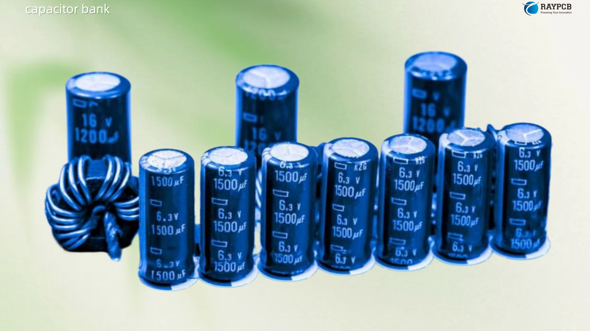
Master decoupling capacitor placement, value selection, and PCB layout best practices โ€” with real engineering formulas, ESR/ESL explained, and a practical placement checklist.

Walk into any PCB bring-up session and watch what the first power-on oscilloscope probe checks. Nine times out of ten, it’s the power rail. Unstable voltage, mystery resets, ADC readings that drift for no apparent reason, microcontrollers stuck in brownout โ€” these symptoms are frequently traced back to a missing, misplaced, or incorrectly valued decoupling capacitor. This guide covers every aspect of decoupling capacitors that matters for real-world PCB design: what they actually do at the physics level, how to pick the right values, where to put them in layout, and the placement rules that actually hold up under scrutiny versus the myths that keep getting repeated in forums.

What Is a Decoupling Capacitor and Why Does Every IC Need One?

A decoupling capacitor โ€” also called a bypass capacitor in many contexts โ€” is a capacitor placed between an IC’s power supply pin and ground, physically close to the component it serves. Its primary job is to act as a local energy reservoir, storing charge and releasing it rapidly when the IC demands a sudden burst of current during a switching event.

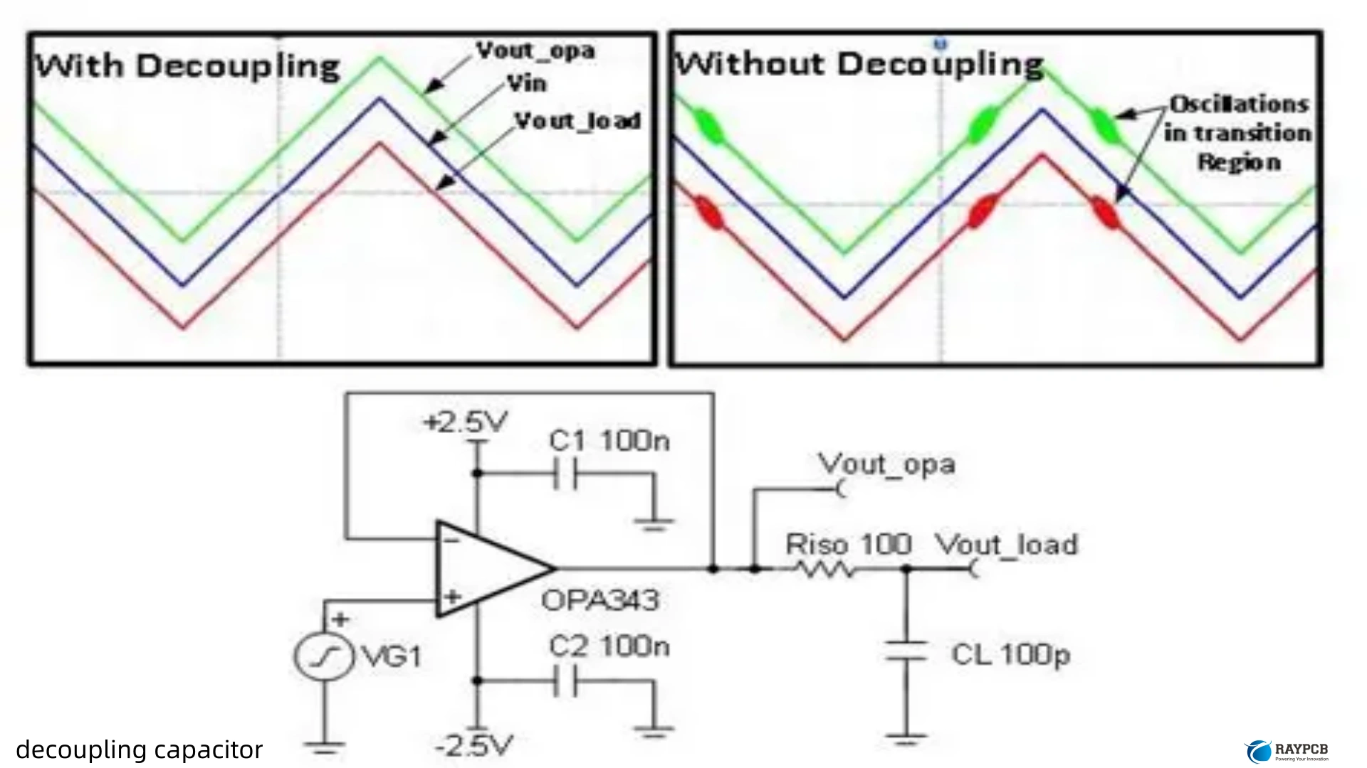
Here is the core problem it solves. When a digital IC switches logic states, it draws a fast transient current spike from the power supply. The PCB traces, vias, and power planes connecting that IC to the main power supply all have inductance. Inductance resists sudden changes in current. So when the IC pulls a spike, the inductance of the supply path creates a temporary voltage dip at the IC’s power pin โ€” a voltage rail sag. If that dip exceeds the IC’s noise margin, you get logic glitches, register corruption, or a full processor reset. Placing a decoupling capacitor directly at the power pin means the capacitor โ€” not the distant power supply โ€” provides that transient current spike. The capacitor’s stored charge bridges the gap while the main supply catches up.

The secondary role of a decoupling capacitor is filtering high-frequency noise already present on the power rail. Every switching power supply produces ripple and high-frequency spectral content. Every digital bus creates simultaneous switching output (SSO) noise. A well-placed decoupling capacitor provides a low-impedance path for this noise to circulate locally rather than coupling into sensitive analog circuits, radiating as EMI, or propagating through the power distribution network (PDN).

Decoupling Capacitor vs. Bypass Capacitor: Is There a Difference?

These terms are often used interchangeably, and in most practical contexts that is fine. Technically, “bypass capacitor” refers to a capacitor that shunts high-frequency noise from an IC’s power pin to ground, while “decoupling capacitor” more precisely refers to a capacitor placed across the power and ground planes to prevent low-frequency rail noise from propagating between sections of the board. In practice, a well-placed 100 nF MLCC near a logic IC serves both functions simultaneously. This guide uses the terms interchangeably, as the industry broadly does.

How a Decoupling Capacitor Works: The Physics Behind It

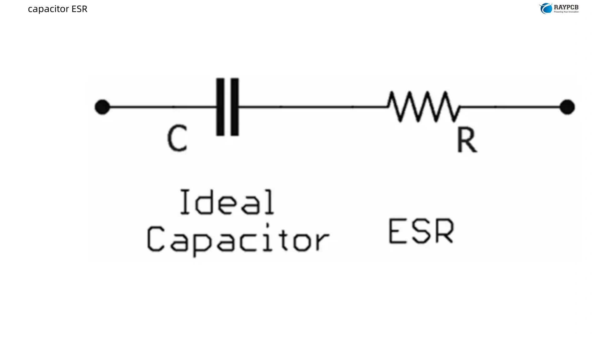
A real capacitor is not an ideal component. It is an RLC network: a capacitor (C) in series with equivalent series resistance (ESR) and equivalent series inductance (ESL). These parasitics fundamentally determine how useful a decoupling capacitor is at any given frequency.

Self-Resonant Frequency (SRF)

Every decoupling capacitor has a self-resonant frequency (SRF) โ€” the frequency at which the capacitive reactance and the inductive reactance (from ESL) cancel each other out. At the SRF, the capacitor’s impedance reaches its minimum value, which is set by the ESR alone. This is the frequency where the decoupling capacitor is most effective.

Below the SRF: the component behaves as a capacitor โ€” impedance falls as frequency rises. Above the SRF: the ESL dominates โ€” impedance rises as frequency rises, and the component starts behaving like an inductor.

This is why a 100 ยตF electrolytic capacitor does not help suppress 100 MHz noise. Its SRF might be around 1โ€“2 MHz. At 100 MHz it is already inductive and contributing nothing useful. The correct tool for 100 MHz noise is a small MLCC (e.g., 100 nF or 10 nF in a 0402 package) whose SRF falls in the tens to hundreds of MHz range.

ESR and ESL: What the Datasheet Numbers Actually Mean

ESR (equivalent series resistance) sets the floor for how low the capacitor’s impedance can get at resonance. Lower ESR means lower minimum impedance, which means more effective noise suppression. MLCCs have ESR in the single-digit milliohm range. Aluminum electrolytic capacitors can have ESR of hundreds of milliohms, which is why they are poor choices for high-frequency decoupling despite their large capacitance values.

ESL (equivalent series inductance) determines where the SRF sits and how fast the impedance rises above it. Typical ESL for an 0402 MLCC is around 0.5โ€“1 nH. A through-hole electrolytic can be 10โ€“20 nH. Every millimeter of PCB trace between the capacitor and the IC power pin adds approximately 1 nH of additional mounting inductance on top of the component’s own ESL. A standard via adds another 0.5โ€“1.5 nH depending on board thickness. This is the reason placement matters as much as component selection.

Capacitor TypeTypical ESRTypical ESLSRF RangeBest Decoupling Frequency
MLCC 100 nF (0402)5โ€“30 mฮฉ0.5โ€“1 nH30โ€“150 MHz10โ€“200 MHz
MLCC 1 ยตF (0402)5โ€“30 mฮฉ0.5โ€“1 nH10โ€“50 MHz5โ€“100 MHz
MLCC 10 ยตF (0805)5โ€“50 mฮฉ1โ€“2 nH3โ€“15 MHz1โ€“30 MHz
Tantalum 10 ยตF100โ€“500 mฮฉ2โ€“5 nH1โ€“5 MHz100 kHzโ€“5 MHz
Al Electrolytic 100 ยตF50โ€“300 mฮฉ10โ€“20 nH100โ€“500 kHz1 kHzโ€“1 MHz
Al Polymer 100 ยตF5โ€“30 mฮฉ5โ€“10 nH300 kHzโ€“2 MHz10 kHzโ€“5 MHz

Decoupling Capacitor Values: What to Use and Why

The Classic Three-Tier Decoupling Strategy

Effective decoupling across a wide frequency range requires multiple capacitor values because no single component covers all frequencies well. The industry-standard approach uses three tiers of capacitance placed at different locations in the power distribution hierarchy.

Tier 1 โ€” Bulk Capacitance (10 ยตF to 100 ยตF): Large electrolytic, tantalum, or polymer capacitors placed near the power supply entry point on the board or near voltage regulators. These handle low-frequency load transients and provide a charge reservoir for the entire board. They compensate for the slow response time of the main power supply.

Tier 2 โ€” Mid-Range Decoupling (1 ยตF to 10 ยตF): MLCC capacitors (X7R dielectric, 0603 or 0805 package) placed near ICs that have moderate switching currents. These bridge the impedance gap between the bulk caps and the local high-frequency decoupling caps.

Tier 3 โ€” Local High-Frequency Decoupling (100 nF to 10 nF): Small MLCCs (0402 or 0201 package, X7R dielectric) placed directly at each IC power pin. These handle fast switching transients and high-frequency noise at the component level. The 100 nF (0.1 ยตF) value is the most universal starting point in digital design and is the standard recommendation from virtually every MCU and FPGA manufacturer.

How Many Decoupling Capacitors Per IC?

The standard rule is one 100 nF MLCC per VDD/VCC power pin, supplemented by one shared mid-range capacitor (1โ€“10 ยตF) per IC. For simple microcontrollers with two or three power pins, this means three to four capacitors per IC. For large FPGAs with dozens of power pins across multiple supply domains, a full decoupling plan following the manufacturer’s application notes is required โ€” these documents usually specify values, quantities, and placement constraints precisely.

An important nuance: if space prevents one capacitor per pin, use a minimum of one 100 nF cap per IC, placed at the power pin cluster that drives the highest-speed internal logic. Shared capacitors are a compromise but are better than no local decoupling.

Calculating Decoupling Capacitance from First Principles

For engineers who need to go beyond rules of thumb, the minimum required capacitance can be estimated from the transient current demand:

C = I ร— ฮ”t / ฮ”V

Where:

  • Iย = the transient current demand of the IC (from the datasheet or simulation)
  • ฮ”tย = the rise/fall time of the switching transient
  • ฮ”Vย = the maximum acceptable voltage droop at the power pin (typically 5% of VDD)

Example: A microcontroller draws a 100 mA transient spike with a 10 ns rise time, and the supply is 3.3 V with a maximum 5% droop (165 mV allowed).

C = 0.1 A ร— 10 ร— 10โปโน s / 0.165 V โ‰ˆ 6 nF

Two parallel 100 nF capacitors significantly exceeds this requirement and also provides lower effective ESL than a single larger cap โ€” good margin for most MCU applications.

Decoupling Capacitor Value Selection by Application

ApplicationRecommended Local DecouplingSupplemental Bulk Cap
3.3V / 5V Logic MCU100 nF X7R MLCC per VDD pin10 ยตF X7R or polymer
FPGA Core Voltage100 nF + 10 nF per power pin clusterPer vendor app note
High-Speed SerDes / DDR100 nF + 1 nF per power pin100 ยตF polymer near rail
Op-Amp Supply Pin100 nF C0G + 10 ยตF tantalumโ€”
RF IC Supply100 pF + 10 nF + 100 nF cascaded10 ยตF near LDO output
Motor Driver VCC100 nF MLCC + 100 ยตF electrolytic220โ€“470 ยตF bulk near driver
Audio DAC/ADC AVDD100 nF C0G (low noise)10 ยตF low-ESR tantalum

Decoupling Capacitor Placement: The Rules That Actually Matter

Placement is where theory meets the reality of a physical PCB, and it is where more designs fall short than in value selection. Correct component selection with poor placement delivers worse results than decent component selection with excellent placement.

The First Law of Decoupling: Minimize Loop Inductance

The single most important placement objective is minimizing the inductance of the current loop formed by the IC power pin, the capacitor, and the return path back through ground. Every element in that loop adds inductance: trace length, via height, trace width, the gap between power and ground vias. Every nanohenry of loop inductance reduces the frequency range over which the capacitor is effective.

A practical trace inductance rule: approximately 1 nH per millimeter of trace length on a typical PCB. This means a decoupling capacitor placed 5 mm away from the IC power pin, with traces routing to reach it, has already added 5 nH of mounting inductance before the capacitor’s own ESL is even counted. At 100 MHz, 5 nH of inductance presents an impedance of over 3 ฮฉ โ€” completely defeating any benefit from the capacitor.

The target: place decoupling capacitors within 1โ€“2 mm of the IC power pin they serve, with the shortest possible trace routing to both power and ground connections.

Placement Strategy by PCB Stack-Up

The effectiveness and optimal placement strategy for decoupling capacitors changes depending on the PCB layer arrangement.

PCBs with tightly coupled power and ground planes (โ‰ค 4 mil / 0.1 mm separation): The interplane capacitance of closely spaced copper planes is significant โ€” approximately 16 pF/cmยฒ for FR-4 at 10 mil spacing, increasing as planes get closer. On a board with tight plane spacing, the planes themselves provide high-frequency decoupling and the exact X/Y position of the discrete capacitors becomes less critical. The parasitic inductance of the plane structure is inherently low and uniformly distributed. This is how dense server motherboards manage to use relatively few bypass capacitors while supporting GHz-class processors.

Typical 4-layer PCBs with standard stack-up (40โ€“60 mil plane separation): The wide interplane gap makes plane capacitance negligible. Discrete capacitor placement is critical. One capacitor per power pin, placed as close as physically possible, is required for reliable operation at high clock speeds.

Two-layer PCBs (no dedicated power planes): Decoupling capacitor placement is critical and the ground return path must be deliberately routed. Use the shortest possible traces, keep the capacitor and IC power pin on the same layer, and route a direct wide trace to the capacitor ground pad and back to the main ground reference. A solid ground pour beneath the decoupling network helps significantly.

Via Placement: The Often-Overlooked Detail

Many engineers get the capacitor placement correct but then add unnecessary inductance through careless via routing. The best practice for connecting a decoupling capacitor to buried power and ground planes:

  • Place the power via and the ground via adjacent to the capacitor padsย โ€” not at the end of a trace stub running from the pad
  • Keep the power and ground vias as close together as possibleย โ€” the distance between them determines the loop area of the current return path through the planes
  • For BGA packages and dense high-speed designs, consider via-in-padย technology to eliminate trace stubs entirely and connect directly to the power ball through the pad
  • Avoid routing any traces between the capacitor pad and the via โ€” the via should be at the edge of the pad or immediately next to it
  • Use multiple viasย per capacitor pad in high-current or high-frequency applications to reduce via inductance in parallel

The Back-Side Placement Technique for BGAs

For BGA packages on multilayer PCBs, placing the decoupling capacitor on the opposite (bottom) side of the PCB directly beneath the BGA can achieve lower loop inductance than placing the capacitor on the top side next to the BGA. The current path from a BGA power ball on the top layer, down through a short via to the bottom-side capacitor, and back through a ground via is often shorter than routing across the top surface to a nearby capacitor. This technique requires via-in-pad or very short stubs on the top side ball pads and is standard practice in high-speed processor board design.

Component Placement Order: Capacitors Before Traces

This sounds obvious but it gets ignored in real design schedules. Place decoupling capacitors before routing any signal traces. Decoupling capacitors should be treated as extensions of the IC package โ€” they belong physically next to the power pins with guaranteed clear routing space. When signal traces are routed first and capacitors are fitted into leftover space, the result is always a layout compromise. The decoupling capacitors end up further away than optimal, connected through convoluted trace paths, and their effectiveness degrades accordingly.

Multiple Capacitors in Parallel: Value Ordering

When using multiple decoupling capacitors of different values on the same power pin โ€” for example, a 100 nF and a 10 nF in parallel โ€” a common question is which capacitor should be closest to the IC. The answer: place the smallest-value capacitor closest to the power pin. The smaller capacitor has a higher SRF and handles the fastest transient currents. It needs the lowest mounting inductance to do its job effectively. The larger capacitor can be slightly further away because it handles slower, lower-frequency transients where a few extra millimeters of trace inductance matters much less.

A caution on anti-resonance: placing two different-value capacitors in parallel creates an anti-resonance peak (impedance spike) at a frequency between the SRFs of the two capacitors. If this peak falls at a critical frequency in your design โ€” such as a major clock harmonic โ€” the parallel combination can actually increase PDN impedance at that frequency. In sensitive designs, use simulation tools to check the parallel impedance profile before committing to the layout.

Common Decoupling Mistakes PCB Engineers Make

Using Electrolytics for High-Frequency Decoupling

An aluminum electrolytic capacitor with 10 nH ESL and a SRF below 500 kHz contributes almost nothing to decoupling at 50 MHz or above. It is the correct choice for bulk energy storage on a power rail, but it should always be supplemented by ceramic MLCCs for local high-frequency bypass. Using only electrolytics near a high-speed IC is one of the most common mistakes in beginner PCB designs.

Putting Decoupling Capacitors on the Wrong Side of Ferrite Beads

If a ferrite bead separates the noisy digital supply from a clean analog supply, the decoupling capacitors for the analog section must be placed after the ferrite bead โ€” on the clean side. Placing them before the ferrite bead means they decouple the noisy digital rail. The whole point of the ferrite bead filter is undermined if the downstream decoupling is missing.

Daisy-Chaining Power Connections Through Capacitor Pads

Some designers route the main power trace through the capacitor pad โ€” the trace runs from the power source, to one pad of the capacitor, continues to the next capacitor pad, and then finally reaches the IC power pin. This series routing means the decoupling capacitor is connected in series with the power path rather than in shunt (parallel) between power and ground. A shunt bypass capacitor must connect from the power node to ground โ€” not in line between the source and the load.

Ignoring the IC Manufacturer’s Application Note

Every IC manufacturer publishes reference designs and application notes for their products. For high-speed processors, FPGAs, and RF ICs, these documents specify not just capacitor values but exact placement constraints, recommended via structures, and bill of materials. Following these recommendations is free high-quality design guidance. Ignoring them in favor of general rules of thumb โ€” when the manufacturer has done the measurements โ€” is a source of unnecessary risk.

Single Decoupling Cap for Multiple Power Pins

Some MCUs have three VDD pins and three GND pins for a reason โ€” each pin supplies a different internal circuit block. Sharing a single 100 nF capacitor across all three VDD pins, placed somewhere between them, compromises the decoupling for all three. Each power pin deserves its own capacitor, placed directly at that pin.

Decoupling Capacitors for Specific Circuit Types

Analog and Mixed-Signal ICs
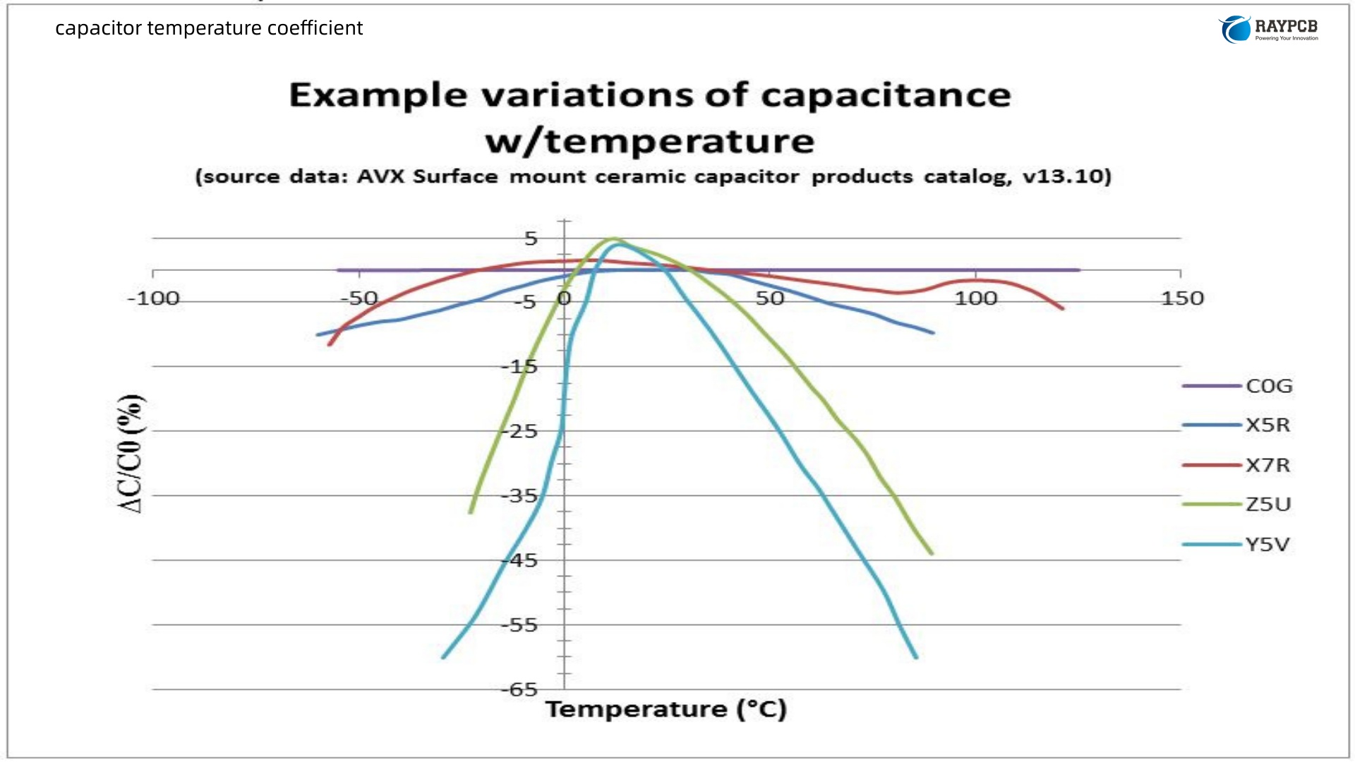
Analog circuits โ€” op-amps, ADCs, DACs, voltage references โ€” are sensitive to power supply noise in ways that digital logic is not. For analog power pins, use C0G/NP0 dielectric MLCCs rather than X7R for the local high-frequency bypass capacitor. C0G’s lower dielectric absorption, non-piezoelectric behavior, and stable capacitance under bias make it superior for keeping precision analog supply pins clean.

A low-noise LDO before the analog supply rail, followed by a 10 ยตF low-ESR tantalum and a 100 nF C0G at each analog power pin, is a solid baseline for precision measurement circuits.

FPGA and High-Speed Processor Decoupling

FPGAs require decoupling across a wide frequency range because internal logic switches simultaneously across millions of flip-flops. Core voltage decoupling for a mid-size FPGA can require dozens of capacitors โ€” 100 nF and 10 nF in combination per power pin cluster. Always start with the official power delivery application note from the FPGA vendor (Xilinx/AMD, Intel/Altera, Lattice). These documents are detailed and board-specific.

RF and Microwave Circuits

RF supply decoupling uses a cascaded approach: a large bulk cap (10 ยตF tantalum or polymer) at the regulator output, followed by progressively smaller ceramics (1 ยตF โ†’ 100 nF โ†’ 10 nF โ†’ 100 pF) as you approach the RF IC power pin. The 100 pF value has an SRF in the low GHz range and handles GHz-frequency supply noise directly at the IC. The cascade creates overlapping low-impedance bands that together cover from kHz to multi-GHz frequencies.

Decoupling Capacitor Best Practices: Quick Reference

Design StepBest Practice
Value selection100 nF X7R MLCC per digital IC power pin; supplement with 1โ€“10 ยตF per IC
Package sizeUse 0402 or 0201 for lowest ESL; avoid 0805 or larger for local bypass
Dielectric (analog)Use C0G/NP0 for precision analog and audio supply pins
PlacementWithin 1โ€“2 mm of IC power pin; on back side of PCB for BGAs
Via placementPower and ground vias directly adjacent to capacitor pads
Trace routingShortest possible traces; wide and direct; no stubs
OrderingSmallest value cap closest to power pin when stacking multiple values
Stack-upTighter plane spacing reduces placement sensitivity for high-freq decoupling
Manufacturer guidanceAlways check and follow the IC vendor’s decoupling application note
SimulationUse PDN simulation for FPGA/high-speed designs to verify impedance profile
Placement timingPlace decoupling caps before routing signal traces
Ferrite beadsPlace decoupling capacitors on the clean side of EMI filters

Frequently Asked Questions

Q1: Can I place my decoupling capacitor far from the IC as long as I use large traces?

No. Trace inductance is dominated by trace length, not trace width, once the width is reasonably wide (above 10 mils for most PCBs). A trace that is twice as wide has roughly half the inductance per unit length โ€” but a trace that is twice as long has twice the inductance regardless of width. The only way to reduce mounting inductance is to shorten the distance between the capacitor and the IC power pin. Wide traces help marginally; short traces help fundamentally.

Q2: Do I need decoupling capacitors if I have a solid, continuous ground plane?

Yes. A good ground plane improves the return path and reduces the loop inductance of the current path, making your decoupling capacitors more effective. But the ground plane does not replace the need for discrete decoupling capacitors. The plane does not store charge in the way a capacitor does, and it cannot supply the instantaneous transient current spikes that digital ICs demand. Both are needed โ€” the ground plane and the discrete capacitors work together.

Q3: My schematic shows 100 nF next to every IC. Does the value matter, or is it just symbolic?

The value matters for frequency coverage. 100 nF has a practical SRF in the range of 30โ€“100 MHz in a typical 0402 package, making it effective for the switching frequencies of most digital logic. For very high-speed circuits (>100 MHz clock domains, GHz SerDes), supplement with a 10 nF or 1 nF capacitor at those specific power pins. For slower MCUs below 50 MHz, 100 nF is usually sufficient as the local bypass without the additional smaller value.

Q4: Why do some IC application notes call for 10 nF and 100 nF in parallel rather than a single 110 nF capacitor?

Because two capacitors with different values have different SRFs and therefore cover different frequency ranges. A 100 nF has its SRF at a lower frequency than a 10 nF. Placing them in parallel creates two impedance minima โ€” one around the SRF of each capacitor โ€” giving broader frequency coverage than a single 110 nF. A single 110 nF capacitor only has one SRF, somewhere between the two, and covers neither frequency band as effectively. The parallel combination also reduces total ESL (two sets of vias in parallel).

Q5: My board has reset problems under high CPU load. Could it be a decoupling issue?

Very likely. Classic symptoms of inadequate power decoupling include: microcontroller resets or hangs under heavy processing load, ADC readings that shift when digital activity increases, oscilloscope measurements showing rail voltage drooping or spiking in time with processor activity, and EMC test failures in the radiated emissions band. Start by probing the IC’s VDD pin directly with a 10:1 probe tip soldered as close to the pin as possible (not through a clip lead). If you see voltage excursions exceeding 5% of VDD correlated with the resets, insufficient or improperly placed decoupling is the likely cause. Add 100 nF MLCCs directly at the VDD pins and retest.

Useful Resources for Decoupling Capacitor Design

ResourceDescriptionLink
Murata SimSurfingSimulate MLCC capacitance, ESR, ESL vs. frequency, temperature, and DC biasds.murata.co.jp/simsurfing
KEMET KSIMModel capacitor impedance with real parasitics under operating conditionsksim3.kemet.com
TDK MLCC SelectorFilter MLCC by capacitance, voltage, case size, dielectric, ESRproduct.tdk.com
AVX (Kyocera) SpiCapDownload SPICE models for AVX MLCCs for PDN simulationavx.com
Digi-Key MLCC FilterFull parametric search including ESR, ESL, SRF fieldsdigikey.com
Altium PDN AnalyzerIntegrated PDN simulation and impedance profiling within Altium Designeraltium.com
Cadence Sigrity PowerSIIndustry-standard PDN analysis and decoupling optimization toolcadence.com
Wรผrth Elektronik RedexpertInteractive MLCC impedance and frequency response tool with real component datawe-online.com/redexpert
Speeding Edge (Lee Ritchey)Technical papers on PDN design, plane capacitance, and decoupling strategyspeedingedge.com
IPC-2141AStandard for high-speed board design including power distribution guidelinesAvailable via IPC.org

Summary

The decoupling capacitor is one of the most consequential passive components in any digital or mixed-signal PCB design, and also one of the most frequently mishandled. The guiding principles:

Every IC power pin needs a local 100 nF X7R MLCC placed as close as physically possible to the pin. Supplement with a 1โ€“10 ยตF mid-range capacitor per IC and a 100 ยตF bulk capacitor near the power entry or voltage regulator. Use additional small-value capacitors (10 nF, 1 nF) at high-speed power pins where clock frequencies exceed 100 MHz.

Placement matters as much as value selection. Every millimeter of trace between the capacitor and the IC power pin adds ~1 nH of mounting inductance, which directly degrades high-frequency decoupling effectiveness. Place capacitors before routing signal traces. Put vias directly at capacitor pads. Use the back side of the PCB for BGA packages.

Always check the IC manufacturer’s application note for specific decoupling recommendations. For FPGAs, high-speed processors, and RF ICs, the vendor’s power delivery guide is the most accurate source of capacitor values, quantities, and placement rules โ€” more reliable than any generic rule of thumb.

Get the decoupling right, and your first power-on oscilloscope measurement will show clean, stable rails. Get it wrong, and the same measurement will explain a lot of debugging sessions you thought were software problems.

Ceramic vs Electrolytic Capacitor: Which Should You Use?

Ceramic vs electrolytic capacitor โ€” a PCB engineer’s guide to ESR, dielectric types, DC bias effects, and exactly which cap to use in every circuit scenario.

If you’ve spent any time routing a PCB or debugging a noisy power rail, you already know that picking the wrong capacitor can cost you days of troubleshooting. The ceramic vs electrolytic capacitor decision comes up in virtually every design โ€” from a simple Arduino power supply to a high-frequency RF front-end. Both capacitor types have earned their place in electronics, but they are fundamentally different animals, and blindly swapping one for the other is a fast track to circuit headaches.

This guide cuts through the noise and gives you a practical, engineer-level breakdown of when to reach for a ceramic, when to stick with an electrolytic, and what to watch out for in both cases.

What Is a Ceramic Capacitor?

A ceramic capacitor uses a ceramic material as its dielectric โ€” the insulating layer sandwiched between two metal electrodes. The most widely used form today is the Multilayer Ceramic Capacitor (MLCC), which stacks hundreds of ceramic and electrode layers to achieve useful capacitance in an extremely small package. A typical 0603 MLCC can pack several microfarads into a footprint smaller than a grain of rice.

Ceramic caps are non-polarized, meaning you can drop them in either direction โ€” no band, no stripe, no risk of explosive failure if you get the orientation wrong.

Ceramic Dielectric Classes: C0G vs X7R vs Y5V

One thing that trips up less experienced engineers: “ceramic capacitor” is not a single spec. The dielectric class dramatically changes how the cap behaves in your circuit.

Class I โ€” C0G / NP0: Paraelectric dielectrics, extremely stable. Temperature coefficient of 0 ยฑ30 ppm/ยฐC across โˆ’55ยฐC to +125ยฐC. Capacitance doesn’t drift with voltage, doesn’t age meaningfully, and dissipation factor stays below 0.15%. These are your precision parts โ€” oscillators, timing circuits, RF matching networks. The tradeoff is lower capacitance density; you won’t find a C0G in anything much above 10 nF in a small package.

Class II โ€” X7R / X5R: Ferroelectric dielectrics based on barium titanate (BaTiOโ‚ƒ). Dielectric constant around 3,000, so you get dramatically more capacitance per unit volume. X7R covers โˆ’55ยฐC to +125ยฐC with ยฑ15% capacitance tolerance over that range. This is the workhorse for decoupling, bypassing, and general filtering. The gotchas: capacitance drops significantly under DC bias (sometimes 40โ€“60% at rated voltage), and there’s measurable aging โ€” X7R loses roughly 1โ€“2% capacitance per time decade.

Class III โ€” Y5V / Z5U: Very high dielectric constant, huge capacitance in a tiny package, but terrible stability. Capacitance can swing ยฑ80% over temperature. Avoid these unless you truly don’t care about the actual capacitance value.

What Is an Electrolytic Capacitor?

An electrolytic capacitor uses an oxide layer (typically aluminum oxide, Alโ‚‚Oโ‚ƒ) as the dielectric, grown electrochemically on an aluminum foil anode. A liquid or solid electrolyte acts as the effective cathode. Rolling this structure into a cylinder gives you the classic can-shaped component you see dominating power supply boards.

The physics of this construction enables very high capacitance in a relatively small body. Electrolytic caps routinely span from 1 ยตF all the way into the thousands of microfarads โ€” territory that ceramics simply can’t match cost-effectively.

The critical catch: electrolytic capacitors are polarized. Connect them backwards and you’re asking for trouble โ€” at best a dead cap, at worst a component that vents or ruptures. The shorter lead (and the stripe on the body) marks the negative terminal. This is non-negotiable.

Ceramic vs Electrolytic Capacitor: Head-to-Head Comparison

ParameterCeramic (MLCC)Electrolytic (Aluminum)
Capacitance Range1 pF โ€“ ~100 ยตF1 ยตF โ€“ 100,000 ยตF+
Voltage RatingUp to several kVTypically 6.3 V โ€“ 500 V
PolarityNon-polarizedPolarized (must observe +/โˆ’)
ESRVery low (mฮฉ range)Higher (can be ฮฉ range)
ESLVery lowHigher
High-Frequency PerformanceExcellentPoor (degrades above ~100 kHz)
Temperature StabilityExcellent (C0G) to moderate (X7R)Moderate; electrolyte degrades at extremes
LifespanDecades (no liquid to dry out)5โ€“20 years typical
PackageSMD (0201 to 2220) or through-hole discThrough-hole can or SMD polymer
Cost (for same value)Higher at large ยตF valuesVery economical for bulk capacitance
Piezoelectric EffectYes (Class II โ€” audible noise possible)No
AC CapableYesNo (DC only, unless non-polarized type)
DC Bias EffectSignificant for X7R/X5R (up to โˆ’60%)Minimal

Key Technical Differences Explained

ESR and High-Frequency Performance

For a PCB designer, ESR (Equivalent Series Resistance) is often the deciding parameter. Ceramic capacitors have extremely low ESR โ€” typically in the single-digit milliohm range. This means they can source and sink high-frequency transient currents with minimal resistive loss.

Electrolytic capacitors carry significantly higher ESR, especially as frequency climbs. Above roughly 100 kHz, the impedance of a standard aluminum electrolytic rises instead of falling, making it nearly useless for high-frequency noise suppression. This is exactly why you see a 100 nF ceramic placed physically next to an IC’s VCC pin even when there’s already a 100 ยตF electrolytic on the board โ€” the ceramic handles the fast transients that the electrolytic can’t touch.

Capacitance vs Voltage (DC Bias Effect)

This is one of the most under-appreciated traps in ceramic cap selection. Class II MLCCs (X7R, X5R) exhibit a strong DC voltage dependence. A 10 ยตF, 10 V X7R MLCC in an 0805 package might only deliver 4โ€“5 ยตF of effective capacitance when biased at 5 V. At 10 V it could be even lower. Electrolytic capacitors don’t suffer from this โ€” their capacitance is far more stable under DC bias.

The practical fix for MLCCs: always derate voltage generously. A common rule of thumb is to use parts rated at 2ร— your operating voltage minimum.

Aging

Class II ceramic caps lose capacitance over time in a predictable logarithmic fashion โ€” typically 1โ€“2% per decade hour for X7R. An electrolytic ages differently; its electrolyte gradually dries out or degrades, which raises ESR and reduces capacitance โ€” but on a longer timescale measured in years. C0G ceramics don’t age meaningfully at all.

Polarity and Orientation Risk

This is operational, not electrical, but it matters on the production floor. Electrolytic capacitors require correct placement orientation every time. A reversed electrolytic in a power supply can fail violently. Ceramics are orientation-agnostic, simplifying PCB assembly and eliminating one category of placement defect entirely.

Mechanical Sensitivity (Ceramic)

Ceramic MLCCs, especially larger case sizes (1206, 1210 and above), are brittle. They can crack under PCB flexure, soldering thermal stress, or board depanelization. A cracked MLCC often presents as an intermittent short โ€” one of the nastier faults to debug. Electrolytics are physically far more robust.

Ceramic Capacitor Dielectric Quick-Reference

Dielectric TypeTemp RangeCapacitance Tolerance (Temp)Best Use Case
C0G / NP0โˆ’55ยฐC to +125ยฐCยฑ30 ppm/ยฐCOscillators, RF, timing, precision filters
X7Rโˆ’55ยฐC to +125ยฐCยฑ15%General decoupling, bypass, filtering
X5Rโˆ’55ยฐC to +85ยฐCยฑ15%Consumer decoupling (lower temp range)
Y5Vโˆ’30ยฐC to +85ยฐC+22% / โˆ’82%Non-critical bypass (unstable)

When to Use a Ceramic Capacitor

Reach for a ceramic when:

Decoupling and Bypass: Every IC power pin should have a ceramic cap โ€” typically 100 nF X7R in 0402 or 0603 โ€” placed as close to the pin as physically possible. The low ESR and low ESL of ceramics make them the right choice for killing high-frequency switching noise before it reaches your IC. For a more in-depth look at how capacitors function on a PCB, including placement strategies and common design pitfalls, it’s worth reviewing the fundamentals before laying out your board.

RF and High-Frequency Circuits: Matching networks, RF coupling, antenna circuits โ€” these always use C0G/NP0 ceramics for their extremely stable impedance and low loss characteristics.

Precision Timing and Oscillators: RC timing circuits and crystal oscillator load capacitors depend on stable capacitance values. X7R’s voltage dependence and aging disqualify it here; C0G is the right call.

Space-Constrained Designs: The volumetric efficiency of MLCCs is unmatched in the sub-10 ยตF range. Wearables, hearing aids, IoT sensors โ€” anywhere board area is precious, ceramics win.

AC Coupling and Signal Path: Non-polarized ceramics work cleanly in AC coupling applications. Electrolytic caps are not suitable for AC signals.

High-Temperature Environments: With the right dielectric (X7R or C0G), ceramics operate reliably at 125ยฐC and beyond. Electrolytic electrolytics degrade faster at elevated temperatures.

When to Use an Electrolytic Capacitor

Reach for an electrolytic when:

Bulk Energy Storage on Power Rails: Linear regulators and switching power supplies need large reservoir capacitors on their output rails. A 470 ยตF or 1000 ยตF electrolytic does this job economically. Replicating this with ceramics would require impractical numbers of MLCCs at much higher cost.

Input Filtering on Power Supplies: Large input capacitance absorbs line ripple and holds up voltage during transient loads. Electrolytics are the standard choice here, typically placed in parallel with a smaller ceramic for high-frequency bypass.

Audio Coupling (Large Signal Path Coupling): Coupling capacitors in audio circuits often need to be in the tens to hundreds of microfarads range to maintain flat frequency response at low frequencies. Electrolytic audio-grade caps (or non-polarized electrolytic types) are the traditional choice.

Low-Frequency Filtering: Below a few kilohertz, the higher ESR of electrolytics is much less of a concern, and the high capacitance values they offer at low cost are hard to beat.

Cost-Sensitive High-Capacitance Designs: If you need 1000 ยตF on a $5 IoT power supply board, an electrolytic is the practical answer. The equivalent ceramic solution would be expensive and physically impractical.

Common Circuit Applications and Recommended Capacitor Type

ApplicationRecommended TypeTypical Value
IC VCC decouplingCeramic X7R100 nF
MCU bulk bypassCeramic X7R or Polymer1โ€“10 ยตF
Power supply output filterElectrolytic (+ parallel ceramic)100โ€“2200 ยตF + 100 nF
RF matching networkCeramic C0G1โ€“100 pF
Crystal oscillator load capsCeramic C0G12โ€“22 pF
Audio signal couplingElectrolytic (non-polarized)10โ€“100 ยตF
Switching regulator input capElectrolytic + Ceramic100 ยตF + 100 nF
EMI filter (Class Y safety cap)Ceramic (Y-rated)1โ€“100 nF
Timing / RC circuitCeramic C0G100 pF โ€“ 10 nF
Motor drive bulk storageElectrolytic1000 ยตF+

Can You Replace an Electrolytic with a Ceramic?

Yes, sometimes โ€” and modern MLCCs have made this increasingly viable at lower capacitance values. Modern high-density X7R MLCCs can now reach 47โ€“100 ยตF in a 1206 package, genuinely competitive with small electrolytic caps. In switched-mode power supplies (SMPS) operating above a few hundred kilohertz, replacing a 47 ยตF electrolytic output cap with several 10 ยตF MLCCs in parallel can dramatically reduce output ripple due to the lower ESR.

However, a direct 1-for-1 substitution requires caution:

  1. Account for DC bias derating โ€” the nominal value printed on the ceramic cap is not what you get at operating voltage.
  2. Check the voltage rating. An 0805 10 ยตF 6.3 V X7R is not a drop-in replacement for a 10 ยตF 25 V electrolytic.
  3. Replacing large bulk electrolytics (100 ยตF+) with ceramics remains expensive and physically impractical for most designs.
  4. The reverse โ€” replacing a ceramic with an electrolytic โ€” almost never works for decoupling or high-frequency roles due to ESR and self-resonance limitations.

A Practical PCB Engineer’s Decision Checklist

Before choosing between a ceramic and electrolytic capacitor, work through these questions:

1. What capacitance value do you need? Under 10 ยตF โ€” ceramic is viable. Over 100 ยตF โ€” electrolytic is likely the practical answer.

2. What is the operating frequency? Above 100 kHz, use ceramics. Below a few kHz, electrolytics are fine.

3. Does polarity matter? In AC circuits, or anywhere orientation errors could occur in production, non-polarized ceramics have an advantage.

4. What are the temperature requirements? For automotive or industrial (โˆ’40ยฐC to 125ยฐC), use X7R ceramics or specifically rated electrolytics.

5. How critical is the actual capacitance value? For precision timing, oscillators, or filters โ€” use C0G. For bulk bypass โ€” value tolerance matters little.

6. What is the board space constraint? Tight SMD layout favors MLCCs. Through-hole electrolytics need clearance for their tall cylindrical bodies.

7. Is noise/EMI a concern? Ceramics near each switching node, electrolytic for bulk.

Useful Resources and Reference Databases

Here are the key references and datasheets databases that any engineer working through the ceramic vs electrolytic capacitor decision should bookmark:

Manufacturer Parametric Search Tools

Standards and Technical References

  • IEC 60384-1ย โ€” Fixed capacitors for use in electronic equipment
  • EIA-198 Standardย โ€” Ceramic capacitor dielectric classification coding
  • MIL-PRF-55681ย โ€” Military spec for ceramic chip capacitors

Learning and Application Notes


Frequently Asked Questions (FAQ)

Q1: Can I use a ceramic capacitor in place of an electrolytic for power supply filtering?

For low-capacitance applications (under ~47 ยตF) in a modern SMPS, modern MLCCs can work well and may actually improve high-frequency ripple performance due to their lower ESR. However, you must account for DC bias derating โ€” a 10 ยตF X7R at its rated voltage may only deliver 4โ€“6 ยตF of effective capacitance. For large bulk filtering (100 ยตF and above), electrolytics remain the practical and cost-effective choice.

Q2: Why does my ceramic capacitor read a much lower value than its label on my LCR meter?

Almost certainly a DC bias effect. If you are measuring an X7R or X5R MLCC with a DC bias applied (which many LCR meters do by default), the ferroelectric dielectric is suppressing effective capacitance. Measure at zero DC bias, or better yet, use a meter that can simulate the operating bias voltage. A 10 ยตF cap measuring as 4 ยตF in circuit is not faulty โ€” it’s physics.

Q3: What causes electrolytic capacitors to bulge or explode?

Three common causes: reverse polarity (the electrochemical reaction accelerates destructively), over-voltage (the oxide dielectric breaks down), and excessive ripple current generating internal heat that dries the electrolyte and builds internal pressure. Always verify polarity, observe voltage derating (typically 80% of rated), and check ripple current specs against your application.

Q4: What is the piezoelectric effect in ceramic capacitors and does it matter?

Class II MLCCs (X7R, X5R, Y5V) use ferroelectric ceramics that are also piezoelectric โ€” they physically deform under applied voltage. In switching power supplies, this can generate audible buzzing (the cap acts like a tiny speaker). In audio circuits, it can introduce noise into the signal path. Solutions: use C0G/NP0 in sensitive audio paths, physically underfill or conformal-coat the board, or select MLCCs with an anti-vibration structure from manufacturers like Murata or TDK.

Q5: How do I choose between an aluminum electrolytic and a polymer electrolytic capacitor?

Polymer electrolytic capacitors use a solid conductive polymer as the electrolyte instead of a liquid. This gives them dramatically lower ESR (approaching MLCCs), better high-frequency performance, and longer lifespan since there’s no liquid to dry out. They’re an excellent middle-ground choice for SMPS output filtering where you need bulk capacitance with better transient response than a standard aluminum electrolytic. The tradeoff is cost โ€” polymer caps are noticeably more expensive than standard aluminum electrolytics of the same capacitance.

Summary: Ceramic vs Electrolytic Capacitor

Neither capacitor type is universally superior โ€” they are complementary tools. In most real-world PCB designs, you’ll use both. The established pattern is: electrolytic capacitors for bulk energy storage and low-frequency filtering on power rails, ceramic capacitors for high-frequency decoupling, precision circuits, RF, and everything where low ESR and stability matter.

When you’re next choosing between ceramic and electrolytic, the fastest decision framework is:

  • Need bulk capacitance (>10 ยตF) at low cost?ย โ†’ Electrolytic
  • Need high-frequency performance, low ESR, small footprint?ย โ†’ Ceramic (X7R)
  • Need precision, stability, RF?ย โ†’ Ceramic (C0G)
  • Need both bulk and transient response?ย โ†’ Electrolytic in parallel with a ceramic

Get that combination right and your power rails will be clean, your ICs will stay happy, and your production line will thank you for the polarity-safe ceramics.

Last updated: 2025 | Written from a PCB engineering perspective for designers working on real-world circuit design challenges.

Capacitor in Series vs Parallel: Formulas & Practical Guide

Learn how capacitors in series and parallel work โ€” formulas, voltage distribution, worked examples, and practical PCB applications. Includes comparison tables and FAQs.

Walk through any PCB schematic and you’ll find capacitors stacked in parallel on every power rail and occasionally chained in series across high-voltage nodes. Both configurations are everywhere, but a surprising number of engineers apply them by habit rather than by calculation. Understanding capacitors in series and in parallel โ€” the formulas, the trade-offs, and the real-world reasons for choosing one over the other โ€” is foundational knowledge that pays dividends every time you sit down to design or debug a board.

This guide covers the math, the physical reasoning behind it, worked examples, and the practical scenarios where each configuration actually makes sense.

Why Capacitor Configuration Matters on a Real PCB

Before diving into formulas, it’s worth framing why this matters beyond textbook theory. When you place capacitors on a PCB, you’re making deliberate choices about total capacitance, voltage handling, energy storage, and impedance behavior across frequency. Getting the configuration wrong doesn’t just mean slightly off filtering โ€” it can mean a regulator that oscillates, a high-voltage rail that destroys components, or decoupling that works at DC but fails completely at the switching frequency where it’s needed most.

Capacitors in Parallel: Formula, Behavior, and When to Use It

H3: The Parallel Capacitance Formula

When capacitors are connected in parallel โ€” all positive terminals tied together, all negative terminals tied together โ€” the total capacitance is simply the sum of each individual capacitance:

C_total = Cโ‚ + Cโ‚‚ + Cโ‚ƒ + … + Cโ‚™

This is the intuitive one. Parallel capacitors add together the same way parallel resistors do not. The reason is physical: placing capacitors in parallel effectively increases the total plate area while keeping the plate separation constant. More plate area means more charge storage โ€” more capacitance.

Worked Example:

Three capacitors in parallel: 100ยตF, 47ยตF, and 10ยตF.

C_total = 100 + 47 + 10 = 157ยตF

That’s it. No reciprocals, no complex algebra.

H3: Voltage Rating in a Parallel Configuration

This is where engineers sometimes get complacent. When capacitors are in parallel, the voltage across every capacitor is identical โ€” it equals the supply voltage. This means:

  • Each capacitor must individually be rated for the full supply voltage
  • The parallel configuration does NOT increase the voltage rating
  • Using a 16V capacitor in parallel with a 50V capacitor on a 24V rail will destroy the 16V cap

The total charge storage increases, and the total energy stored increases, but the voltage limit is set by the weakest component in the group.

ParameterParallel Configuration
Total CapacitanceCโ‚ + Cโ‚‚ + Cโ‚ƒ
Voltage RatingEquals the lowest-rated individual cap
Total ChargeQ_total = Qโ‚ + Qโ‚‚ + Qโ‚ƒ
Total EnergyE = ยฝ ร— C_total ร— Vยฒ
Impedance at frequencyLower (capacitors in parallel reduce ESR too)

H3: Why Engineers Put Capacitors in Parallel

The most common reason is to hit a target capacitance when a single large capacitor isn’t available, isn’t cost-effective, or doesn’t fit the footprint. But there are more nuanced reasons:

Broadband decoupling: Different capacitor types have different self-resonant frequencies (SRF). A 100ยตF bulk electrolytic has good low-frequency impedance but poor high-frequency performance. A 100nF MLCC has a high SRF and handles high-frequency noise. Place them in parallel and the combination handles both frequency ranges. This is why you see a large electrolytic and several small ceramics on every power rail in a well-designed board.

ESR reduction: Parallel capacitors combine their ESR in parallel, reducing the total series resistance. If you need very low ESR for a high-ripple-current application, paralleling multiple standard electrolytics is often cheaper than buying a single premium low-ESR unit.

Reliability / redundancy: In high-reliability designs, spreading capacitance across multiple smaller units reduces the impact of any single component failure.

Capacitors in Series: Formula, Behavior, and When to Use It

H3: The Series Capacitance Formula

Capacitors in series follow the reciprocal sum formula โ€” the same structure as parallel resistors:

1/C_total = 1/Cโ‚ + 1/Cโ‚‚ + 1/Cโ‚ƒ + … + 1/Cโ‚™

Or in the simplified two-capacitor case:

C_total = (Cโ‚ ร— Cโ‚‚) / (Cโ‚ + Cโ‚‚)

The total capacitance of capacitors in series is always less than the smallest individual capacitor. This seems counterintuitive until you understand the physics: series capacitors effectively increase the total plate separation while keeping the plate area constant. Greater separation means lower capacitance.

Worked Example 1 โ€” Two equal capacitors in series:

Cโ‚ = Cโ‚‚ = 100ยตF

C_total = (100 ร— 100) / (100 + 100) = 10000 / 200 = 50ยตF

Two equal capacitors in series always give exactly half the individual capacitance.

Worked Example 2 โ€” Two unequal capacitors in series:

Cโ‚ = 100ยตF, Cโ‚‚ = 22ยตF

C_total = (100 ร— 22) / (100 + 22) = 2200 / 122 = 18.03ยตF

Notice how the result is dominated by the smaller capacitor. In series configurations, the smallest capacitor has the most influence on the total โ€” the opposite of a chain of parallel capacitors.

Worked Example 3 โ€” Three capacitors in series:

Cโ‚ = 10ยตF, Cโ‚‚ = 47ยตF, Cโ‚ƒ = 100ยตF

1/C_total = 1/10 + 1/47 + 1/100 = 0.1 + 0.02128 + 0.01 = 0.13128

C_total = 1 / 0.13128 = 7.62ยตF

H3: Voltage Distribution in Series Capacitors

This is the critical behavior that makes series configurations useful. When capacitors are connected in series, the supply voltage divides across the capacitors in inverse proportion to their capacitance:

Vโ‚ = V_total ร— (C_total / Cโ‚)

Or equivalently, since charge is equal on all series capacitors:

Vโ‚ / Vโ‚‚ = Cโ‚‚ / Cโ‚

A smaller capacitor takes a larger share of the voltage. A larger capacitor takes a smaller share.

Voltage distribution example:

Two capacitors in series across a 100V supply: Cโ‚ = 100ยตF, Cโ‚‚ = 100ยตF

Vโ‚ = Vโ‚‚ = 50V each โ€” equal split for equal capacitances.

Now with Cโ‚ = 100ยตF, Cโ‚‚ = 10ยตF:

C_total = (100 ร— 10) / 110 = 9.09ยตF Vโ‚ = 100 ร— (9.09 / 100) = 9.09V across the 100ยตF cap Vโ‚‚ = 100 ร— (9.09 / 10) = 90.9V across the 10ยตF cap

The smaller capacitor takes the majority of the voltage. This is why unmatched capacitors in series without voltage-balancing resistors are dangerous.

ParameterSeries Configuration
Total CapacitanceLess than smallest individual cap
Voltage RatingSum of individual voltage ratings (with caveats)
Voltage DistributionInversely proportional to capacitance
ChargeEqual on all capacitors (Q = C_total ร— V_total)
Primary Use CaseVoltage rating extension, AC coupling, charge pumps

H3: Voltage Balancing Resistors in Series Capacitor Strings

If you’re putting electrolytic capacitors in series to handle a higher voltage than a single unit supports, you must add balancing resistors in parallel with each capacitor. Without them, manufacturing tolerances and leakage current differences will cause the voltage to distribute unevenly, potentially over-stressing one capacitor in the string.

The balancing resistor value is typically chosen so that the bleed current (V/R) is roughly 3โ€“5ร— the maximum expected capacitor leakage current. A common starting point is 100kฮฉ for capacitors rated below 100V, but always verify against the specific capacitor’s leakage spec in the datasheet.

Series vs Parallel: Direct Comparison

PropertyCapacitors in SeriesCapacitors in Parallel
Total CapacitanceLess than smallest capSum of all caps
Voltage HandlingHigher (sum of ratings*)Same as individual rating
Formula1/C_t = 1/Cโ‚ + 1/Cโ‚‚…C_t = Cโ‚ + Cโ‚‚ + Cโ‚ƒ…
Charge StoredSame on each capDivides among caps
ESRAdds (higher total ESR)Reduces (lower total ESR)
Main ApplicationVoltage extension, AC couplingIncreased capacitance, broadband filtering
Risk FactorUnequal voltage sharingIndividual cap voltage ratings

*Only achievable reliably with matched capacitors or balancing resistors.


Practical PCB Applications: When to Use Series or Parallel

H3: Parallel Capacitors for Power Supply Decoupling

The textbook example: on a 3.3V rail, you’ll commonly see a 10ยตF X5R MLCC in parallel with a 100nF C0G MLCC. The 10ยตF handles mid-frequency bulk charge storage, the 100nF handles high-frequency transient decoupling near its self-resonant frequency. The combination gives flat, low-impedance coverage across a decade or more of frequency.

This is not just parallel capacitance addition โ€” it’s strategic impedance engineering across frequency. When you’re laying out the board, the 100nF decoupling cap should be as close as physically possible to the IC power pin, with the 10ยตF cap slightly further out toward the power plane. The placement reinforces the frequency-domain division of labor between the two.

H3: Parallel Capacitors to Meet Bulk Capacitance Targets

On a 12V input switching converter that calls for 470ยตF of input capacitance, you have choices: one large 470ยตF/25V unit, two 220ยตF/25V units in parallel, or four 100ยตF/25V units in parallel. In high-ripple-current designs, the multiple-unit approach distributes thermal load and can be mechanically more reliable. The total ESR of four paralleled caps is one-quarter the individual ESR, which matters when you’re calculating power dissipation in the capacitor bank.

H3: Series Capacitors for Voltage Rating Extension

A common scenario in industrial or automotive electronics: you need 200ยตF at 100V, but your approved component list only has 63V-rated electrolytics in the right footprint. Two 470ยตF/63V caps in series give you approximately 235ยตF at an effective 126V rating (with balancing resistors). This is a real solution used in production hardware when lead times or cost constraints make single high-voltage units impractical.

H3: Series Capacitors for AC Coupling

AC coupling capacitors โ€” used to block DC while passing AC signals โ€” are almost always single capacitors, but the principle of series capacitance applies when you need a specific coupling capacitance in an unusual value. More relevantly, the series capacitor in an AC coupling application must be chosen with regard to the RC time constant it forms with the load resistance, which defines the low-frequency cutoff of the coupling network.

H3: Series-Parallel Combinations for Custom Requirements

Real designs sometimes call for series-parallel combinations. For example, a 4-capacitor array might be arranged as two parallel groups of two series capacitors each. The calculation proceeds in stages: resolve the series groups first to get their equivalent capacitance, then sum the parallel results.

Example:

Group A: 100ยตF and 100ยตF in series โ†’ 50ยตF Group B: 100ยตF and 100ยตF in series โ†’ 50ยตF Group A in parallel with Group B โ†’ 100ยตF at 2ร— the individual voltage rating

This configuration doubles the voltage handling compared to all four in parallel, while maintaining 100ยตF total capacitance โ€” a useful trade-off when board space is fixed but voltage headroom is needed.

Capacitance, Energy, and Charge: The Supporting Equations

For completeness, here are the core capacitor equations that apply in both configurations:

FormulaDescription
Q = C ร— VCharge stored (Coulombs)
E = ยฝ ร— C ร— VยฒEnergy stored (Joules)
I = C ร— (dV/dt)Current in response to voltage change
X_C = 1 / (2ฯ€ ร— f ร— C)Capacitive reactance at frequency f
f_SRF = 1 / (2ฯ€ ร— โˆš(LC))Self-resonant frequency (L = parasitic inductance)

The reactance formula is particularly important for decoupling design. A 100nF capacitor has a reactance of about 1.6ฮฉ at 1MHz and 0.16ฮฉ at 10MHz. Doubling the capacitance (two in parallel) halves the reactance โ€” directly reducing AC impedance at every frequency.

Common Mistakes When Combining Capacitors

Using mismatched caps in series without balancing resistors. Manufacturing tolerance alone can cause significant voltage imbalance. In a 100V system, a 20% capacitance mismatch could result in one capacitor seeing 60V while the other sees 40V โ€” fine if both are rated for 100V, catastrophic if you chose 50V-rated parts.

Assuming series capacitors double the voltage rating. They can, but only with proper balancing. Unbalanced series capacitors in a real circuit will not split voltage evenly, and the component with lower capacitance (which takes more voltage due to Q = CV) may exceed its rating.

Ignoring ESR when paralleling capacitors. Two capacitors in parallel have lower combined ESR only if they’re of similar types. Paralleling a low-ESR MLCC with a high-ESR general-purpose electrolytic creates a complex interaction at resonance. At certain frequencies the circuit can actually exhibit higher impedance than either component alone โ€” a phenomenon called anti-resonance. Simulation in SPICE before layout is good practice on sensitive rails.

Over-decoupling with too many parallel ceramics. More parallel capacitance isn’t always better. Dense MLCC arrays on high-speed power rails can create low-impedance paths that cause instability in some voltage regulator topologies. Check the regulator’s stability requirements and output impedance specifications before stacking caps indiscriminately.

Useful Resources

  • Murata SimSurfingย โ€” product.murata.comย โ€” Simulate capacitance vs. DC bias, temperature, and frequency for Murata MLCCs; essential for parallel decoupling design
  • KEMET SPICE Modelsย โ€” kemet.comย โ€” Downloadable SPICE models including parasitic inductance and ESR for accurate series/parallel simulation
  • TDK Capacitor Selection Toolย โ€” product.tdk.comย โ€” Filter by capacitance, voltage, ESR, and temperature coefficient
  • Texas Instruments Power Supply Decoupling Application Note SLVA630ย โ€” Practical guidance on parallel capacitor selection for IC power pins
  • Digi-Key Capacitor Parametric Searchย โ€” digikey.comย โ€” Filter and compare by series, value, voltage, and ESR
  • EEVblog Capacitor Seriesย โ€” YouTube โ€” David Jones’ practical video series covering capacitor behavior in real circuits
  • All About Circuits โ€” Capacitors Chapterย โ€” allaboutcircuits.comย โ€” Free textbook-quality reference with worked examples

FAQs: Capacitors in Series and Parallel

Q1: Do capacitors in series increase or decrease total capacitance? They decrease it. The total capacitance of capacitors in series is always less than the smallest individual capacitor in the string. The formula is 1/C_total = 1/Cโ‚ + 1/Cโ‚‚ + 1/Cโ‚ƒ. This is the opposite behavior from resistors โ€” series capacitors behave like parallel resistors mathematically.

Q2: Can I simply put two capacitors in series to double the voltage rating? In theory, yes โ€” if both capacitors are identical and matched. In practice, manufacturing tolerances mean the voltage will not split exactly equally, and the capacitor with slightly lower capacitance will carry a higher voltage. For any serious high-voltage application, always add balancing resistors in parallel with each capacitor in the series string to enforce equal voltage sharing.

Q3: Why do PCB designers put a small ceramic capacitor in parallel with a large electrolytic? It’s not just for extra capacitance โ€” it’s for broadband impedance control. A large electrolytic has good low-frequency capacitance but poor high-frequency performance due to its internal inductance and ESR. A small MLCC has a high self-resonant frequency and handles GHz-range noise. Together, the parallel combination gives low impedance across a much wider frequency range than either could achieve alone.

Q4: What happens to the voltage across capacitors when they are connected in parallel? All capacitors in parallel share the same voltage โ€” the voltage across the parallel combination. Each capacitor must be individually rated to handle that full voltage. Connecting a lower-voltage capacitor in parallel with a higher-rated one on a rail that exceeds the lower rating will damage or destroy the underrated component.

Q5: How do I calculate total capacitance for a mixed series-parallel network? Work from the inside out. Resolve any series groups to their equivalent single capacitance using the reciprocal formula. Then treat those equivalent values as single components and resolve the parallel combinations by addition. Repeat until you have a single equivalent capacitance. Drawing the circuit as a simplified schematic at each stage helps avoid errors in complex networks.

Final Thoughts

Whether you’re designing a decoupling network, extending voltage headroom, or just trying to hit a target capacitance from stock components, knowing the series and parallel capacitor formulas cold is non-negotiable. The math for capacitors in series is exactly where engineers expect the opposite โ€” less capacitance, higher voltage handling โ€” while parallel combinations give you the intuitive result of summed capacitance with shared voltage stress.

The formulas are just the entry point. The real engineering judgment is knowing when each configuration serves the circuit, how ESR and self-resonance interact in parallel arrays, and when a series string needs balancing resistors to stay safe. Get those right, and your capacitor selection choices will hold up from simulation through production.

Capacitor Voltage Rating: How to Choose & Derate Correctly

Learn how to choose the right capacitor voltage ratingย and derate correctly by type โ€” MLCC, electrolytic, tantalum, and film โ€” with tables, worked examples, and derating rules every PCB engineer needs.

Every PCB engineer has been there โ€” you grab a 16V electrolytic for a 12V rail and think, “16 is greater than 12, we’re good.” Then six months into field deployment, you get a batch of failures. The problem wasn’t the capacitance value. It was the capacitor voltage rating and how it was applied.

This guide cuts through the confusion. We’ll cover what capacitor voltage rating actually means, how different capacitor types behave under voltage stress, the correct derating rules for each type, and the real-world mistakes that cause premature failures on production boards.

What Is a Capacitor Voltage Rating?

The capacitor voltage rating โ€” often printed as WV (Working Voltage) or WVDC (Working Voltage DC) โ€” defines the maximum continuous voltage that can be safely applied across the capacitor’s terminals without degrading the dielectric or causing failure.

It is not a hard cliff where everything below is fine and everything above instantly fails. It’s more of a stress threshold. Operating near the rated voltage accelerates dielectric aging, increases leakage current, and in some capacitor types dramatically reduces effective capacitance. Operating well below the rated voltage extends service life significantly.

The voltage rating is established by the manufacturer based on:

  • The dielectric material’s breakdown field strength
  • The dielectric layer thickness
  • Acceptable capacitance stability within the rated range
  • Long-term reliability targets at rated temperature

One critical point most engineers miss: the voltage rating is a starting point for design, not a safe operating limit.

Why Exceeding the Capacitor Voltage Rating Causes Failure

When voltage stress approaches or exceeds the rated maximum, several degradation mechanisms kick in simultaneously.

Dielectric breakdown is the primary failure mode. The insulating layer between the capacitor plates begins to conduct, creating leakage paths that widen over time. In ceramic capacitors this can result in a low-resistance short. In electrolytic capacitors it causes the oxide layer to rupture.

Increased leakage current follows from partial dielectric breakdown. Current flowing through the dielectric generates heat internally, which further accelerates degradation โ€” a self-reinforcing failure loop.

Overheating is particularly pronounced in electrolytic capacitors, where excess voltage causes internal heating that accelerates the evaporation of the liquid electrolyte, shrinking the effective capacitance and eventually causing venting or rupture.

Physical damage differs by type: electrolytic capacitors may bulge, leak, or burst; ceramic capacitors may crack internally or arc between layers; tantalum capacitors can enter catastrophic thermal runaway.

Capacitor Voltage Rating by Type: What You Need to Know

Not all capacitors respond to voltage stress in the same way. Understanding the failure characteristics of each type is the foundation for correct derating.

Ceramic Capacitors (MLCCs)

Ceramic capacitors are the most common passive component on virtually any modern PCB. Their non-polarized construction makes them versatile for AC and DC circuits, but their voltage behavior is more complex than most engineers realize.

The key issue is the voltage coefficient of capacitance (VCC). Class II ceramics using high-K dielectrics such as BaTiOโ‚ƒ (X7R, X5R, Y5V) experience significant capacitance loss as the applied DC voltage approaches the rated voltage. In the worst cases โ€” particularly Y5V dielectric parts โ€” capacitance can drop by 80% or more at the rated voltage. An MLCC labeled 10ยตF may only provide 2โ€“4ยตF at its full working voltage.

X7R capacitors are significantly better behaved than Y5V, but still experience notable DC bias-induced capacitance reduction. Always check the manufacturer’s DC bias derating curves โ€” the datasheet nominal capacitance value is measured at 0V DC bias, not at your operating voltage.

Beyond capacitance loss, fast voltage transients within the rated voltage limit can also degrade ceramic dielectrics over time, even when peak voltages stay below the maximum.

Aluminum Electrolytic Capacitors

Aluminum electrolytics use an oxide layer on aluminum foil as the dielectric. This oxide layer is formed electrochemically and its thickness โ€” and therefore the voltage rating โ€” is directly proportional to the formation voltage used during manufacturing.

These capacitors are polarized. Reverse voltage events, even brief ones from supply sequencing or inductive back-EMF, damage the oxide layer and reduce voltage rating. Repeated small reverse voltage events accumulate as latent damage before catastrophic failure.

Capacitor lifetime in aluminum electrolytics is strongly voltage-dependent and even more strongly temperature-dependent. The Arrhenius relationship means that every 10ยฐC increase in operating temperature roughly halves the service life. When voltage stress and thermal stress combine, lifetime reduction is multiplicative.

Tantalum Capacitors

Tantalum capacitors offer excellent volumetric efficiency and stable electrical parameters, but they carry a uniquely hazardous failure mode that demands respect. When tantalum pentoxide dielectric breaks down under voltage stress, localized defects can develop into conducting filaments. The subsequent current flow generates intense heat, and the tantalum-MnOโ‚‚ combination can sustain an exothermic reaction โ€” sometimes producing smoke and flame.

Traditional MnOโ‚‚ tantalum capacitors require 50% voltage derating with no exceptions in commercial designs. This is not a conservative recommendation โ€” it reflects the actual failure physics of the component. Polymer tantalum capacitors have a safer failure mode and require less derating (10โ€“20%), but they should not be treated as drop-in replacements without verifying ESR and circuit stability.

Inductive loads on rails where tantalum capacitors are used for decoupling are a serious design hazard. Inductive kick from relay coils, motor windings, or solenoids frequently generates transients that exceed the 50% derating limit even when the nominal rail voltage appears safe.

Film Capacitors

Polypropylene and polyester film capacitors have a valuable property: self-healing. A localized dielectric puncture causes the metallized electrode to vaporize around the fault, clearing it and restoring insulation. This allows film capacitors to survive occasional transient overvoltage events that would destroy ceramic or electrolytic types.

However, each self-healing event consumes electrode material and slightly reduces capacitance. Sustained operation near the rated voltage exhausts the self-healing capacity over time. Film capacitors in AC mains applications should be specifically rated for AC use (X-rated or Y-rated safety capacitors) โ€” a DC voltage rating is not equivalent.

Voltage Derating Rules: A Practical Reference Table

The following table summarizes standard voltage derating guidelines by capacitor type. These reflect typical commercial design practice; safety-critical, aerospace, and mil-spec applications often apply stricter derating.

Capacitor TypeStandard DeratingNotes
Ceramic (Class II: X7R, X5R)50% of rated voltageCheck DC bias curves for actual capacitance at operating voltage
Ceramic (Class I: C0G/NP0)25โ€“50% of rated voltageMore stable under voltage; lower derating acceptable
Ceramic (Y5V)Avoid if possibleSevere capacitance loss; consider X7R or better
Aluminum Electrolytic80% at 25ยฐC; 60โ€“70% at 85ยฐCElectrolytic aging doubles per 10ยฐC; check ripple current limits
Tantalum MnOโ‚‚50% for all applicationsNo exceptions; risk of thermal runaway above this threshold
Tantalum Polymer10% for Vr โ‰ค 10V; 20% for Vr > 10VSafer failure mode; confirm ESR compatibility
Film (polypropylene/polyester)50โ€“70% for DC circuitsSelf-healing but finite; check AC vs DC rating
Supercapacitors / EDLCs75โ€“80% of rated voltageElectrolyte decomposition accelerates above rated voltage

How to Calculate the Correct Capacitor Voltage Rating for Your Circuit

Selecting the correct capacitor voltage rating is not as simple as finding the nominal supply voltage and picking a part above that value. The actual peak voltage across the capacitor must be calculated, then derating applied on top.

Step 1: Identify the True Peak Voltage

For DC circuits with ripple โ€” such as power supply output filters or DC bus capacitors in switching regulators โ€” the peak voltage is:

V_peak = V_DC + V_ripple_peak

For AC circuits, remember that RMS voltage is not peak voltage. A 230V AC mains circuit has a peak voltage of 230 ร— โˆš2 = 325V. A DC-rated capacitor placed in this circuit would need to be rated for at least 325V DC, with derating applied on top.

For circuits with transient events โ€” inductive loads, hot-plug, load switching โ€” add a transient margin based on your measured or simulated worst-case spike.

Step 2: Apply the Appropriate Derating Factor

Once you have the true peak voltage, apply the derating percentage for your capacitor type from the table above.

Minimum rated voltage = V_peak รท derating factor

Example for a ceramic bypass capacitor on a 3.3V rail with up to 200mV ripple:

  • V_peak = 3.3V + 0.2V = 3.5V
  • 50% derating: minimum rated voltage = 3.5V รท 0.5 = 7V
  • Select a 10V rated MLCC (next standard value above 7V)

Example for a tantalum on a 5V rail:

  • V_peak including transients = 5.5V (conservative estimate)
  • 50% derating: minimum rated voltage = 5.5V รท 0.5 = 11V
  • Select a 16V rated tantalum capacitor

Step 3: Verify Temperature Derating

If the capacitor operates above 85ยฐC, consult the manufacturer’s voltage-temperature derating curves. Most standard-grade aluminum electrolytics are only rated for 80โ€“85% of their full voltage at maximum temperature. At 85ยฐC ambient with self-heating from ripple current, you may be looking at effective body temperatures of 95ยฐC or higher, which requires additional voltage margin or improved thermal management.

Step 4: Check DC Bias Curves for Ceramic Capacitors

For MLCC decoupling capacitors, confirm that the actual capacitance at your operating voltage meets your circuit’s requirements. Use the manufacturer’s simulation tools โ€” Murata SimSurfing, TDK Product Advisor, Samsung SPEC โ€” to pull the DC bias derating curve for the specific part you’re considering.

A 10ยตF X7R MLCC at 10V rated voltage may only provide 5โ€“6ยตF at 3.3V operating voltage. If your design needs a reliable 10ยตF for bulk decoupling, you may need a 22ยตF or 47ยตF rated part to achieve that effective capacitance in circuit.

Capacitor Voltage Rating Selection: Worked Examples

The following table shows how derating works in common design scenarios.

ApplicationRail VoltageTransients / RippleCapacitor TypeMinimum Rated VRecommended Selection
3.3V logic decoupling3.3V~100mV rippleMLCC X7R7V10V MLCC, check DC bias at 3.3V
5V rail bulk filter5V~500mV rippleAluminum electrolytic13.75V16V or 25V electrolytic
5V rail decoupling (tantalum)5VInductive load transientsTantalum MnOโ‚‚โ‰ฅ12V16V tantalum; add transient suppression
12V rail bulk filter12V1V ripple, thermal stress at 75ยฐCAluminum electrolytic32.5V (with thermal)35V or 50V at 105ยฐC rating
230V AC mains filter230V RMS (325V peak)Mains transientsX2 film capacitorAC-rated 275V+Use X2-rated film, not DC-rated
48V telecom bus48VSupply transients to 60VFilm or high-V ceramic150V+100V or 200V film or ceramic

Common Capacitor Voltage Rating Mistakes (and How to Fix Them)

Mistake 1: Choosing the Rated Voltage Based on Nominal Supply Voltage Alone

Selecting a 16V electrolytic for a 12V rail looks reasonable on paper. But if the 12V rail has 1V of switching ripple, inrush transients, and operates with the capacitor body at 75ยฐC, the effective voltage stress and thermal stress combined dramatically reduce service life. Bump the voltage rating to 25V or 35V.

Mistake 2: Ignoring DC Bias Derating in MLCCs

The most commonly missed specification in ceramic capacitor selection. A 10ยตF 0402 X7R rated at 10V is almost certainly providing less than 5ยตF at your 3.3V or 5V operating voltage. Always pull the DC bias curve from the manufacturer’s simulation tool โ€” never trust the nominal value alone.

Mistake 3: Using the Same Derating for All Tantalum Types

MnOโ‚‚ tantalum and polymer tantalum have very different failure modes and derating requirements. Over-derating polymer tantalum forces you into unnecessarily high voltage ratings, reducing available capacitance in a given package size. Under-derating MnOโ‚‚ tantalum is a fire risk.

Mistake 4: Forgetting Reverse Voltage on Polarized Capacitors

Aluminum electrolytic and tantalum capacitors have essentially zero reverse voltage tolerance. Supply sequencing errors, hot-plug events, and back-EMF from inductive loads are all real sources of brief reverse voltage. In circuits where reverse voltage is possible, use non-polarized capacitors or add protective diodes.

Mistake 5: Applying DC Ratings to AC Circuits

A capacitor rated 250V DC is not suitable for 230V AC mains use. Peak AC voltage is 325V, and continuous AC stress on a DC-rated capacitor is a different degradation mechanism entirely. Use properly rated X1, X2, Y1, or Y2 safety capacitors for any connection across or to mains voltages.

Temperature and Voltage Derating: How They Interact

Voltage and temperature stress do not add linearly โ€” they multiply. A capacitor running at 70% of rated voltage at room temperature may have a comfortable service life. The same capacitor at 70% voltage with a body temperature of 85ยฐC from ripple current self-heating has dramatically shorter life, because the Arrhenius temperature acceleration factor and the voltage stress acceleration factor apply simultaneously.

For aluminum electrolytic capacitors in enclosed power electronics:

  • At 75ยฐC body temperature: apply 60% voltage derating
  • At 85ยฐC body temperature: apply 50% voltage derating
  • Above 85ยฐC body temperature: improve thermal management first, then address voltage derating

For ceramic capacitors, elevated temperature increases dielectric aging rate and leakage current under voltage stress. High-reliability designs should always consult the manufacturer’s voltage-temperature derating curves rather than assuming the rated voltage applies uniformly across the full temperature range.

Capacitor Voltage Rating for AC Circuits: A Special Case

When a capacitor operates in an AC circuit or in a DC circuit with substantial AC ripple, peak voltage โ€” not RMS or average voltage โ€” is the relevant stress parameter.

For a DC rail with AC ripple, peak voltage = V_DC + V_AC_peak. For a pure AC circuit, peak voltage = V_RMS ร— โˆš2. The capacitor’s voltage rating, with derating applied, must exceed the peak instantaneous voltage at all times.

Safety capacitors (X and Y types) carry additional requirements beyond voltage rating. X2 film capacitors rated at 275V AC account for continuous AC voltage stress including peaks. These ratings are established through rigorous safety certification testing and should never be substituted with DC-rated equivalents in mains-connected designs.

Useful Resources for Capacitor Voltage Rating Research

The following tools and documents are directly useful for real design work:

ResourceTypeUse Case
Murata SimSurfingOnline simulation toolMLCC DC bias derating curves, impedance vs. frequency
TDK Product AdvisorComponent databaseDC bias, temperature characteristics for TDK MLCCs
Kemet K-SIMSPICE simulationCapacitor SPICE models including parasitics
Nichicon Selection ToolAluminum electrolytic databaseLifetime calculations, ripple current derating
Vishay Polymer Derating Guide (PDF)Application notePolymer vs. MnOโ‚‚ tantalum derating comparison
NASA NEPP MLCC Rating Guide (PDF)Technical paperMLCC derating for high-reliability applications
IPC-9592BIndustry standardRequirements for power conversion devices
MIL-STD-981Military standardCapacitor derating for mil-spec designs
Manufacturer datasheetsPrimary sourceAlways check voltage-temperature curves for specific part numbers

FAQs: Capacitor Voltage Rating

Q1: Can I use a higher voltage-rated capacitor than required?

Yes, and in most cases it improves reliability. A higher voltage rating means less dielectric stress at your operating voltage, which extends service life. The trade-offs are size and cost โ€” higher voltage ratings generally require a larger physical package for the same capacitance value. For MLCC decoupling capacitors, going to a higher voltage rating in the same package often means less capacitance, so check the specific part’s DC bias curve before assuming a higher-voltage part is a direct substitute.

Q2: What happens if a capacitor exceeds its voltage rating briefly?

The answer depends heavily on capacitor type and severity. Brief transient exceedance by a few percent for microseconds may cause no immediate damage in film capacitors (which self-heal) but can create latent damage in ceramic and electrolytic types. Sustained operation above rated voltage โ€” even by 10โ€“20% โ€” accelerates dielectric degradation progressively. Significant overvoltage (30%+ above rated) typically causes rapid failure: electrolytic capacitors vent or rupture, tantalum capacitors can catch fire, ceramic capacitors develop low-resistance shorts.

Q3: Does a higher voltage rating improve the actual capacitance value I get in circuit?

For ceramic capacitors: yes, significantly. Because DC bias derating is less severe at a lower percentage of rated voltage, a higher-voltage-rated MLCC will deliver more of its nominal capacitance at your operating voltage. For example, a 10ยตF 25V X7R may deliver 8โ€“9ยตF at 5V, while a 10ยตF 10V X7R might only deliver 5โ€“6ยตF at the same voltage. This is one of the strongest practical arguments for voltage derating in MLCC selection beyond just reliability concerns.

Q4: How do I derate a capacitor for high-temperature environments?

Consult the manufacturer’s voltage-temperature derating curves for the specific component โ€” do not interpolate from general guidelines alone. For aluminum electrolytics, a useful approximation is to reduce the voltage derating by an additional 10% for every 20ยฐC above 85ยฐC ambient. For ceramic capacitors, elevated temperature increases dielectric aging rate; use X7R or C0G dielectrics rather than X5R or Y5V in designs exceeding 85ยฐC ambient. Tantalum capacitors operating above 85ยฐC require additional voltage margin beyond the standard 50% derating.

Q5: Is voltage derating different for switching power supply applications?

Yes. Switching power supply circuits introduce AC ripple voltage, fast transients from switching transitions, and inrush current events that do not exist in simple DC bias applications. The peak voltage across output filter capacitors must account for ripple amplitude in addition to DC bias. For bulk output capacitors and ceramic decoupling on switching regulator outputs, apply the standard derating rules to the peak voltage including ripple, not the nominal DC output voltage. Also verify that ripple current does not exceed the capacitor’s rated ripple current โ€” this is an independent failure mechanism from voltage stress.

Summary: Capacitor Voltage Rating Derating Quick Reference

Getting capacitor voltage rating selection right comes down to three things: knowing the true peak voltage in your circuit (not just the nominal supply), applying the correct derating percentage for your capacitor technology, and verifying that thermal conditions do not require additional margin on top of voltage derating.

Use 50% derating for ceramic MLCCs and MnOโ‚‚ tantalum capacitors as a baseline. Apply more conservative derating for high-temperature environments. Always check DC bias derating curves for MLCC parts โ€” nominal capacitance values are measured at zero DC bias and are almost never what you get in circuit. And never apply a DC voltage rating to an AC circuit application.

A component that costs a few cents more in a higher voltage rating or physically larger package is orders of magnitude cheaper than a field failure, a warranty return, or a safety incident. Choose the voltage rating correctly the first time.

Capacitor Temperature Coefficient: NP0, X7R & Y5V Explained

Understand capacitor temperature coefficientย codes โ€” NP0, X7R, and Y5V decoded, compared, and applied correctly in PCB design with real data and selection tables.

Walk into any electronics lab and you will find the same debate replaying itself: someone swapped an X7R for a Y5V to hit a cost target, and now the circuit behaves strangely above 60ยฐC. Or worse โ€” a product passed room-temperature testing, went through six months of production, then returned from the field with mysterious failures in cold-climate deployments.

The root cause in both cases is almost always the same: the capacitor temperature coefficient was not properly understood or specified.

This is not an exotic failure mode. It is one of the most routine and preventable sources of circuit instability in PCB design, and it affects both new graduates and experienced engineers who have been selecting ceramic capacitors for years based on habit rather than datasheet discipline.

This guide explains exactly what the capacitor temperature coefficient means, how to decode the three-character EIA code from any MLCC datasheet, what the real-world behavior of C0G/NP0, X7R, and Y5V actually looks like, and how to choose the right dielectric for your application the first time.

What Is a Capacitor Temperature Coefficient?

The capacitor temperature coefficient describes how much the capacitance value changes as temperature rises or falls from a standard reference point (typically 25ยฐC). It quantifies the sensitivity of the dielectric material to thermal variation.

For Class I ceramics, the temperature coefficient is expressed in parts per million per degree Celsius (ppm/ยฐC) โ€” a precise, linear description of capacitance drift. For Class II and Class III ceramics, it is expressed as a percentage change over a specified temperature range, and the relationship is nonlinear and far less predictable.

Why does this matter in practice? Because every capacitor in your design sits inside a thermal environment it never experienced on the characterization bench. A board in an automotive ECU may see โˆ’40ยฐC on a cold start and +105ยฐC at the engine control module after an hour on the highway. A board in consumer electronics may sit in a parked car in summer and hit 85ยฐC. If the capacitors selected for timing, filtering, or power conditioning change their values by 30%, 50%, or even 80% across that temperature range, the circuit behavior changes with them.

How to Read the EIA Temperature Coefficient Code

The EIA (Electronic Industries Alliance) standard defines a three-character code for Class II and Class III ceramic capacitors that encodes three pieces of information directly into the part description. Class I types use a separate coding system, with C0G being the dominant example.

Decoding the Three-Character Code

Each character in the code has a specific meaning:

First character (letter): Sets the lower operating temperature limit.

LetterMinimum Temperature
Xโˆ’55ยฐC
Yโˆ’30ยฐC
Z+10ยฐC

Second character (number): Sets the upper operating temperature limit.

NumberMaximum Temperature
4+65ยฐC
5+85ยฐC
6+105ยฐC
7+125ยฐC
8+150ยฐC

Third character (letter): Specifies the maximum allowable capacitance change over the entire temperature range from minimum to maximum.

LetterMaximum ฮ”C/Cโ‚€
Pยฑ10%
Rยฑ15%
Sยฑ22%
T+22% / โˆ’33%
U+22% / โˆ’56%
V+22% / โˆ’82%

So X7R means: operating range from โˆ’55ยฐC to +125ยฐC, with a maximum capacitance change of ยฑ15% across that range. Y5V means: operating range from โˆ’30ยฐC to +85ยฐC, with a maximum capacitance change of +22% to โˆ’82%. The asymmetry in that last figure โ€” +22% upside and โˆ’82% downside โ€” should immediately communicate that Y5V capacitors are dramatically unstable dielectrics.

C0G and NP0: The Precision Standard

What C0G and NP0 Actually Mean

C0G and NP0 are two designations for the same dielectric type. C0G is the EIA standard code; NP0 is the designation used in U.S. military specifications (MIL-PRF-55681), where NP0 stands for Negative-Positive-Zero, describing the essentially flat temperature response. In some European documentation, the designation is written as NPO. In all three cases, the underlying dielectric and performance standard are equivalent.

Both designations specify a temperature coefficient of ยฑ30 ppm/ยฐC or better over the โˆ’55ยฐC to +125ยฐC range. To put that in perspective: across the full 180ยฐC temperature span from minimum to maximum operating temperature, the total capacitance change is less than ยฑ0.54%. This is not just stable โ€” it is remarkably stable, and it is the fundamental reason C0G/NP0 is specified in every application where capacitance stability matters to circuit function.

The Physics Behind C0G Stability

C0G dielectrics are based on titanium dioxide (TiOโ‚‚) with various rare-earth oxide additives including neodymium, samarium, and other elements. Unlike barium titanate-based dielectrics, TiOโ‚‚ does not exhibit ferroelectric behavior. There are no polarizable domains that can be aligned by an electric field and no phase transitions near room temperature that cause abrupt capacitance changes.

The result: the dielectric constant of C0G ceramic does not meaningfully change with temperature, applied voltage, or time. This means C0G capacitors also have essentially zero voltage coefficient of capacitance (no DC bias effect) and negligible aging.

C0G Limitations: The Volumetric Efficiency Trade-Off

The dielectric constant (K) of C0G ceramics is typically in the range of 20โ€“100, compared to values of 3,000โ€“18,000 for Class II ferroelectric dielectrics. This difference means that for any given package size, C0G capacitors cannot achieve high capacitance values. C0G is practical for values in the picofarad to low nanofarad range and up to a few hundred nanofarads in larger packages. Finding a C0G capacitor above 100nF in a 0402 package is essentially impossible. Finding one at 10ยตF in any SMD package is not realistic.

When to Use C0G/NP0

C0G is the correct choice for:

  • Crystal oscillator load capacitors, where even small capacitance shifts change the oscillation frequency
  • RF tuning and matching networks, where capacitance precision directly affects frequency response
  • Precision RC timing circuits used in analog control loops or timing applications
  • Anti-aliasing filters and signal-path capacitors in ADC and DAC circuits
  • Any capacitor position where a ยฑ15% swing in capacitance would cause a circuit specification to be violated across temperature

X7R: The PCB Engineer’s Workhorse

What X7R Actually Guarantees

X7R is the most commonly specified Class II dielectric for general-purpose MLCC use. The code tells us: operating range from โˆ’55ยฐC to +125ยฐC, with a maximum capacitance change of ยฑ15% anywhere in that range. The dielectric constant for X7R is typically around 3,000, which is why X7R parts can be found in the microfarad range in small packages.

The X7R temperature characteristic is specified as a maximum tolerance band. The actual capacitance curve over temperature is nonlinear โ€” it typically has a broad, shallow hump shape across the operating range, with the largest deviations occurring at the temperature extremes. It is not a constant percentage offset from nominal at every temperature; it is a curve that stays within the ยฑ15% guardbands across the full range.

X7R and Voltage Coefficient: The Necessary Warning

X7R’s temperature coefficient specification says nothing about voltage behavior. Engineers sometimes assume that selecting X7R guarantees stable capacitance under all operating conditions. It does not.

X7R capacitors exhibit significant DC bias-induced capacitance reduction โ€” the same fundamental problem as all Class II ferroelectric dielectrics โ€” though less severely than X5R or Y5V. An X7R capacitor at its rated voltage may retain only 30โ€“50% of its nominal capacitance. This is a separate effect from temperature coefficient and must be evaluated independently. The temperature coefficient code tells you how the capacitance varies with temperature at a fixed voltage (typically 0V bias). It tells you nothing about voltage-induced changes.

X7R Aging Rate

Class II ceramic capacitors lose capacitance over time as ferroelectric domains relax toward lower-energy states. For X7R, the aging rate is typically 1โ€“2% per time decade โ€” meaning approximately 1โ€“2% capacitance loss between the first and tenth hour, another 1โ€“2% between the tenth and hundredth hour, and so on. For most commercial designs with product lifetimes of thousands of hours, this aging accumulates to perhaps 5โ€“10% over the product lifetime and is usually within acceptable margins. Designs where this matters should account for aging in the worst-case analysis.

When to Use X7R

X7R is the correct choice for:

  • Bypass and decoupling capacitors in logic power rails, where ยฑ15% capacitance variation across temperature is acceptable
  • Switching regulator output filter capacitors where loop stability is verified with effective capacitance (accounting for DC bias)
  • General-purpose signal coupling and AC blocking where precision is not required
  • Any application operating up to 125ยฐC that needs more capacitance per package than C0G can provide

X5R: X7R’s Lower-Temperature Sibling

X5R uses the same ยฑ15% capacitance change specification as X7R but is only rated to +85ยฐC rather than +125ยฐC. The dielectric constant is similar to or slightly higher than X7R, allowing similar capacitance density. X5R capacitors typically exhibit greater DC bias sensitivity than X7R because the ferroelectric formulation is optimized for higher capacitance density rather than stability.

X5R is appropriate for consumer electronics and low-voltage applications in controlled-temperature environments โ€” 3.3V and 5V rails in desktop computers, mobile devices, and similar products where ambient temperatures above 85ยฐC are not expected. For automotive, industrial, and other elevated-temperature applications, X7R is the correct choice because X5R is simply not rated for the operating temperature range.

Y5V: What the Datasheet Is Actually Telling You

Y5V Temperature Behavior in Plain Numbers

Y5V is a Class II ferroelectric dielectric with extremely high dielectric constant โ€” typically 10,000โ€“18,000 โ€” which enables the highest capacitance values per package size of any common MLCC type. A 100ยตF capacitor in a practical SMD package is possible only with Y5V or similar high-K dielectrics.

The cost is severe instability. The EIA specification for Y5V allows capacitance to change from +22% to โˆ’82% across the temperature range of โˆ’30ยฐC to +85ยฐC. In practice, this means at the upper end of the operating range (85ยฐC), a Y5V capacitor may retain only 18โ€“30% of its nominal room-temperature capacitance. At cold temperatures, it rises above nominal before falling off sharply at the temperature extremes.

This is not a manufacturing defect or a corner-case failure. This is the designed, specified, and tested behavior of Y5V dielectric. A 4.7ยตF Y5V capacitor rated for 6.3V and operated at 5V, 85ยฐC, will in fact deliver approximately 0.33ยตF of effective capacitance โ€” about 14 times less than the label states. This figure, published by Analog Devices, is representative of real Y5V behavior and not an outlier.

Why Y5V Exists at All

Y5V has a valid use case in a narrow application window: non-critical bulk decoupling in consumer electronics that operates close to room temperature, where cost, size, and BOM simplicity outweigh precision. Mass-produced consumer gadgets, cheap toys, and similar products sometimes use Y5V because it provides the highest capacitance per cent in the smallest package. At room temperature with low DC voltage, it does function adequately as a bypass capacitor โ€” it just cannot be relied upon to remain functional across temperature or voltage variation.

For any serious design โ€” industrial control, automotive electronics, medical devices, communications infrastructure, test equipment โ€” Y5V is unsuitable for any position where the capacitance value affects circuit performance. The temperature coefficient alone eliminates it from any application where the product must operate reliably outside a narrow band around room temperature.

Side-by-Side Comparison: C0G vs X7R vs X5R vs Y5V

ParameterC0G / NP0X7RX5RY5V
EIA ClassIIIIIII (High-K)
Dielectric constant (K)20โ€“100~3,000~3,000โ€“4,00010,000โ€“18,000
Operating temp rangeโˆ’55ยฐC to +125ยฐCโˆ’55ยฐC to +125ยฐCโˆ’55ยฐC to +85ยฐCโˆ’30ยฐC to +85ยฐC
ฮ”C over temp rangeยฑ0.54% (ยฑ30 ppm/ยฐC)ยฑ15%ยฑ15%+22% / โˆ’82%
DC bias effectNoneModerateSignificantSevere
Aging rateNegligible~1โ€“2%/decade~1โ€“2%/decade>5%/decade
Max practical capacitance (SMD)~1ยตF (large package)Up to 47ยตFUp to 100ยตFUp to 100ยตF
Typical max package1210 or larger for >100nF0402 and larger0402 and larger0402 and larger
AEC-Q200 automotive qualified?YesYesConditionallyNo
Suitable for precision circuits?YesWith cautionNoNo
Suitable for automotive/industrial?YesYesNo (>85ยฐC)No
Price relative to X7RHigherBaselineSimilarLower

Real-World Temperature Coefficient Impact on Common Circuits

Understanding the temperature coefficient matters most when you think through what it does to specific circuit functions:

RC Timing Circuits

An RC oscillator or timing network produces a time constant ฯ„ = R ร— C. If the capacitor is Y5V and temperature changes by 40ยฐC, the capacitance can drop by 50% or more. The time constant drops by the same percentage, directly shifting the operating frequency, trigger threshold, or timeout period. For any precision timing application โ€” watchdog timers, frequency-setting resistor-capacitor networks, or oscillator circuits โ€” C0G is the only defensible choice.

Power Supply Filtering and Decoupling

For bypass capacitors on digital logic supply rails, ยฑ15% variation from X7R is generally acceptable. The capacitor is providing low-impedance decoupling for transient load currents, and a 15% change in capacitance has a minimal impact on this function as long as adequate total capacitance remains on the rail. X7R is appropriate here.

For switching regulator output filter capacitors, the temperature coefficient combines with DC bias loss, meaning the effective capacitance could be 30โ€“50% lower than nominal at elevated temperature and operating voltage combined. This must be verified with actual derating curves, not estimated from the temperature coefficient code alone.

Anti-Aliasing and Signal-Path Filters

A low-pass filter with a โˆ’3 dB cutoff frequency set by an RC or LC network has a cutoff that is directly proportional to 1/C. If the capacitor value drifts ยฑ15% with temperature, the cutoff frequency shifts by approximately ยฑ15% as well. Whether this is acceptable depends entirely on the filter specification. For a wide-tolerance anti-aliasing filter this may be fine; for a precision measurement channel in a data acquisition system it is almost certainly not. Use C0G for signal-path filter capacitors in any precision application.

RF Matching and Tuning Networks

At RF frequencies, small capacitors set impedance matching conditions and resonant frequencies. A 5 pF capacitor in a 2.4 GHz antenna matching network that changes by even 1โ€“2% with temperature can shift the resonant frequency by tens of megahertz. C0G is the only ceramic dielectric type used in RF tuning applications. The ยฑ30 ppm/ยฐC coefficient of C0G produces frequency shifts that are manageable; X7R with ยฑ15% capacitance variation would make precise RF tuning impossible.

Capacitor Temperature Coefficient Selection Guide by Application

ApplicationRecommended DielectricReason
Crystal oscillator load capacitorsC0G / NP0Any capacitance shift changes oscillation frequency
RF tuning and matchingC0G / NP0Frequency stability requires ppm-level C precision
Precision RC timingC0G / NP0Time constant directly proportional to capacitance
ADC/DAC input filteringC0G / NP0Cutoff frequency must be stable across temperature
Logic decoupling (3.3V, 5V)X7Rยฑ15% acceptable; verify DC bias curves
Switching regulator output filterX7R (verify DC bias)X5R insufficient above 85ยฐC; check effective C
Industrial/automotive decouplingX7R (AEC-Q200)X5R not rated beyond 85ยฐC
Consumer bulk decoupling (non-critical)X5R or X7RCost trade-off; X5R acceptable in benign environments
High-capacitance bypass (cost-critical)Y5V only if C stability non-criticalAcceptable at room temp only; never in industrial/auto
High-frequency RF bypassC0G (low value)Stable at frequency; no DC bias effect

The Automotive Special Case: AEC-Q200 and Capacitor Temperature Rating

Automotive electronics introduces a demanding combination of requirements that makes the capacitor temperature coefficient directly critical to product approval. AEC-Q200 is the qualification standard for passive components in automotive applications, and it requires that MLCCs demonstrate specified performance across the full automotive temperature range.

For powertrain and under-hood applications, the required operating temperature range is typically โˆ’40ยฐC to +125ยฐC or even +150ยฐC. This immediately eliminates X5R (rated only to +85ยฐC) from these applications, and it demands X7R at minimum. High-temperature automotive applications use specialized dielectrics โ€” some manufacturers offer X8R (to +150ยฐC) or equivalent proprietary grades โ€” that extend the stable operating range beyond standard X7R limits.

Y5V capacitors do not meet AEC-Q200 requirements for automotive applications. Their โˆ’30ยฐC lower temperature limit fails to cover the โˆ’40ยฐC automotive cold-start requirement, and their โˆ’82% worst-case capacitance variation is incompatible with any safety-critical or performance-critical function in a vehicle.

Common Mistakes When Specifying Capacitor Temperature Coefficient

The most frequent errors engineers make when dealing with temperature coefficients are not obscure edge cases โ€” they are routine decisions made without enough information:

Treating all X7R parts as equivalent. X7R is a performance specification, not a material recipe. Two different manufacturers’ X7R capacitors of the same nominal value and package can have meaningfully different temperature coefficient curves within the ยฑ15% band, different DC bias behavior, and different aging rates. When qualifying an alternative source, re-verify behavior at operating temperature and voltage โ€” do not assume equivalence from the EIA code alone.

Using X5R in elevated-temperature environments. X5R has the same ยฑ15% tolerance band as X7R but is only specified to +85ยฐC. Equipment that operates in enclosures, near heat sources, or in outdoor summer environments can easily exceed 85ยฐC. Specifying X5R because it offers slightly higher capacitance density in a given package and then deploying the product in a warm environment is a reliability problem waiting to develop.

Specifying Y5V in circuits that operate outside 20โ€“30ยฐC. A Y5V capacitor in a consumer product that spends most of its life between 10ยฐC and 35ยฐC may deliver acceptable performance. The same capacitor in a product that sees โˆ’10ยฐC in winter or +60ยฐC in a car can behave as if the capacitor barely exists. Never use Y5V for anything other than non-critical bulk decoupling in controlled-temperature environments.

Confusing temperature coefficient with overall capacitance stability. The temperature coefficient code specifies only one dimension of capacitance variation. Voltage coefficient (DC bias), aging, and manufacturing tolerance all contribute independently. A complete capacitance budget must account for all four: manufacturing tolerance + temperature drift + DC bias loss + aging. In a worst-case analysis, these factors multiply โ€” not add.

Useful Resources for Capacitor Temperature Coefficient Research

ResourceTypeWhy It’s Useful
Murata SimSurfingOnline simulation toolEnter temperature, voltage, frequency to get actual capacitance curves for any Murata MLCC
TDK Product AdvisorComponent databaseTemperature coefficient curves and DC bias data for TDK MLCCs
Kemet K-SIMSPICE simulationFull SPICE models including temperature and DC bias behavior for Kemet parts
Knowles Capacitor Fundamentals SeriesTechnical article seriesThorough explanation of dielectric classifications, aging, and loss mechanisms
Analog Devices: Temperature and Voltage Variation of Ceramic CapacitorsTechnical articleReal measured data on Y5V and X7R capacitance at operating conditions with no-holds-barred analysis
Passive Components Academy: MLCC StabilityTechnical articleCombined treatment of temperature, bias, and aging with real vendor data
Samsung SPEC ToolComponent databaseDC bias and temperature characteristics for SEMCO MLCCs
AEC-Q200 Standard Summary (JEDEC)Industry standardAutomotive passive component qualification requirements
Manufacturer datasheetsPrimary sourceAlways check the ฮ”C/C vs. temperature curve for your specific part โ€” EIA codes are guaranteed minimums, not descriptions of actual curves

FAQs: Capacitor Temperature Coefficient

Q1: C0G and NP0 โ€” are they the same part? Can I substitute one for the other?

Yes, they are electrically equivalent. C0G is the EIA designation; NP0 is the MIL designation. Both specify a temperature coefficient of ยฑ30 ppm/ยฐC over the โˆ’55ยฐC to +125ยฐC range, no significant DC bias effect, and negligible aging. Some manufacturers use both terms, and TDK uses them to distinguish slightly different temperature ranges for their internal product line โ€” NP0 extended to +150ยฐC versus C0G at +125ยฐC. Unless your application requires the extended temperature range, they are interchangeable. When substituting any component, confirm the voltage rating, package, and capacitance tolerance in addition to the dielectric code.

Q2: My X7R capacitor says ยฑ15% temperature coefficient. Does that mean the capacitance is always within 15% of the nominal value?

The ยฑ15% is the maximum allowable capacitance change from the value measured at 25ยฐC, measured at any temperature within the rated range (โˆ’55ยฐC to +125ยฐC for X7R). It does not account for DC bias-induced capacitance reduction or manufacturing tolerance. A capacitor at the edge of its manufacturing tolerance (typically ยฑ10% or ยฑ20%), under DC bias, and at the temperature extreme could have an effective capacitance substantially below 15% of nominal โ€” all without violating any specification. This is why worst-case analysis for critical capacitor positions must combine all four sources of variation: tolerance + temperature drift + DC bias + aging.

Q3: Why does Y5V even exist if its capacitance is so unstable?

The honest answer is that Y5V maximizes capacitance density at minimum cost for applications that only care about bulk bypass function at or near room temperature. A Y5V capacitor that provides 100ยตF in a 0805 package at room temperature may only deliver 20ยตF at 85ยฐC, but for a non-critical decoupling application in a consumer product that rarely sees temperatures above 40ยฐC, it might be “good enough” โ€” and it costs less than equivalent X7R or X5R parts. The problem is that this trade-off is only valid within a very narrow set of conditions, and those conditions are rarely documented explicitly in design requirements. When the operating environment is undefined or variable, Y5V’s instability becomes a reliability liability rather than a cost saving.

Q4: Can I use the temperature coefficient code to compare capacitors from different manufacturers?

You can use it to confirm that two parts meet the same minimum stability specification โ€” but not to assume they have identical temperature behavior. The EIA code guarantees the outer bounds of performance; it does not specify the shape of the capacitance-versus-temperature curve within those bounds. Two X7R capacitors from different manufacturers can have very different actual temperature curves while both remaining within ยฑ15%. For critical applications, always verify the actual temperature coefficient curve from the manufacturer’s simulation tool or datasheet graphs, not just the EIA code.

Q5: I need more capacitance than C0G can provide in my package size, but I need better stability than X7R offers. What are my options?

Several options exist depending on your specific requirements. First, consider X7S or X8R dielectrics โ€” some manufacturers offer these as proprietary grades with tighter temperature tolerance than X7R while achieving higher capacitance density than C0G. Second, consider polymer tantalum or aluminum polymer capacitors, which offer stable capacitance with essentially no temperature coefficient or DC bias effects, in large-value ratings well above what C0G can provide. Third, review whether a slightly larger package size for a C0G part could achieve adequate capacitance for your application โ€” C0G is available up to several microfarads in 1210 packages from some manufacturers. Fourth, if the capacitance variation is the primary concern and DC bias is manageable, X7R with careful DC bias and temperature derating at the system level may still meet your specification.

Summary: Choosing the Right Capacitor Temperature Coefficient

The capacitor temperature coefficient is not a secondary specification to be noted and forgotten โ€” it is a primary performance parameter that directly determines whether your circuit meets its specifications across the operating temperature range.

C0G/NP0 is for precision. Use it anywhere that capacitance stability over temperature directly matters to circuit function: oscillators, timing, RF, precision analog. X7R is the general-purpose workhorse for decoupling, filtering, and bulk bypass across a wide temperature range โ€” use it for most positions that C0G cannot serve economically, but always verify DC bias behavior for voltage-sensitive applications. X5R offers similar performance to X7R in benign thermal environments and is appropriate for consumer electronics that stay below 85ยฐC. Y5V belongs only in non-critical bulk decoupling in controlled-temperature consumer products, and it should never appear in industrial, automotive, medical, or any precision application.

The three-character EIA code is your starting point โ€” not your complete answer. Read the actual temperature coefficient curve in the datasheet, check the DC bias derating, and budget all sources of capacitance variation together before signing off on a component selection that your circuit will depend on across its entire operating life.

Capacitor Polarity: How to Identify Positive & Negative Leads

Learn to identify capacitor polarity on electrolytic, tantalum & SMD types. Covers markings, PCB silkscreen symbols, multimeter testing & common polarity mistakes.

If you’ve spent any time on the bench debugging a blown PCB, there’s a decent chance a backwards electrolytic capacitor was somewhere in the story. Capacitor polarity is one of those fundamentals that trips up beginners and occasionally bites experienced engineers too โ€” especially when you’re staring at a 105ยฐC bulk capacitor with worn markings under fluorescent lighting at midnight.

This guide walks through everything you need to know: what capacitor polarity means, which capacitor types are affected, how to read the physical markings, how to interpret PCB silkscreen symbols, and how to test polarity with a multimeter when the markings are gone.

What Is CapacitorArity and Why Does It Matter?

Capacitor polarity refers to the orientation requirement of certain capacitors โ€” specifically, which terminal must connect to the higher voltage (positive) and which must connect to the lower voltage (negative or ground). Install one the wrong way around and you’re looking at reduced capacitance, excessive leakage current, internal gas buildup, and in worst-case scenarios, a capacitor that vents, bulges, or explodes.

This isn’t theoretical. Reversed electrolytic capacitors are a leading cause of field failures in consumer electronics power supplies. The damage is often silent at first: the cap degrades over weeks before the circuit starts misbehaving.

Not all capacitors are polarized. The distinction is critical before you even pick up your soldering iron.

Polarized vs. Non-Polarized Capacitors

Understanding which capacitor types require correct polarity orientation is step one.

Capacitor TypePolarized?Typical Use Case
Aluminum Electrolyticโœ… YesBulk power filtering, decoupling
Tantalum (solid)โœ… YesLow-profile power filtering
Niobium Oxideโœ… YesAlternative to tantalum
Ceramic (MLCC)โŒ NoHigh-frequency decoupling
Film (polyester, polypropylene)โŒ NoAudio, timing, filtering
MicaโŒ NoRF, precision circuits
Supercapacitor / EDLCโœ… YesEnergy storage, backup power
Bipolar ElectrolyticโŒ NoAudio crossovers (special case)

The key takeaway: if it has an electrolyte inside โ€” liquid or solid โ€” it almost certainly has a polarity requirement. Ceramics and films are inherently symmetric and can be placed in either direction.

How to Identify Capacitor Polarity: The Markings Explained

H3: Through-Hole Electrolytic Capacitors

Through-hole aluminum electrolytics are the easiest to read once you know the conventions. Manufacturers use multiple overlapping cues, which helps when one marking gets obscured.

Negative stripe: The most universal marking is a prominent stripe โ€” usually white or light gray โ€” running vertically along the body of the capacitor. This stripe marks the negative (โˆ’) lead. The stripe typically contains repeated “โˆ’” symbols or chevrons pointing toward the negative terminal.

Lead length: On a brand-new, untrimmed capacitor, the longer lead is positive (+). This mirrors the convention used for LEDs and diodes. Once leads are trimmed during assembly, this method becomes unreliable โ€” use the stripe instead.

Flat side on the base: Some capacitors (especially smaller radial types) have a slight flat edge on the bottom plastic ring, indicating the negative terminal side.

Markings summary table:

Marking MethodPositive (+) IndicatorNegative (โˆ’) Indicator
Lead length (untrimmed)Longer leadShorter lead
Body stripeOpposite sideStripe side
Base flatOpposite sideFlat edge side
Printed symbol“+” printed on body“โˆ’” or stripe

H3: SMD Electrolytic Capacitors (Radial SMD / Can Style)

Surface-mount aluminum electrolytics follow the same stripe convention but the implementation varies slightly. Look for:

  • A notch or indentย on the top of the can โ€” this marks the negative terminal
  • A light-colored stripeย on the body wrapping toward the negative pad
  • PCB silkscreen will show a “+” marker on the positive land

Because SMD electrolytics are tiny, always cross-reference with the PCB silkscreen before soldering.

H3: Tantalum Capacitors (Through-Hole and SMD)

Tantalum capacitors are the exception to the “stripe = negative” rule that trips people up constantly.

Through-hole tantalum: The longer lead is positive, and the positive terminal is usually marked with a “+” symbol directly on the body. Some older teardrop-shaped tantalums have a band at the positive end โ€” the opposite of electrolytic convention.

SMD tantalum (chip style): A line or bar marking at one end indicates the POSITIVE terminal. This is the reverse of what you’d expect coming from electrolytic experience. The positive end often has a colored band or a stripe on the top of the component. This catches engineers out regularly.

Capacitor TypeStripe/Band Meaning
Aluminum ElectrolyticStripe = NEGATIVE
Tantalum SMDStripe/Bar = POSITIVE
SupercapacitorStripe = NEGATIVE (follows electrolytic)

Commit that table to memory. The tantalum reversal has caused more than a few smoke-testing incidents.

H3: Supercapacitors (EDLCs)

Supercapacitors follow the same convention as aluminum electrolytics: the stripe indicates the negative terminal, and the longer lead (when untrimmed) is positive. Given that supercapacitors can store significant energy, reversed installation isn’t just a component failure โ€” it can be a safety hazard.

Reading Capacitor Polarity on a PCB

Even if you can’t read the component markings clearly, the PCB itself carries polarity information.

H3: Silkscreen Symbols

The silkscreen layer on a properly designed PCB will indicate polarity in several ways:

  • A “+” symbolย next to or inside the component footprint pad
  • A filled or shaded semicircleย inside the circular outline โ€” the filled half indicates the negativeย side (this is the most common electrolytic symbol)
  • A longer line on one padย in the component outline
  • Some designs add explicit “+” and “โˆ’” labels on the copper or silkscreen

H3: Component Footprint in PCB Design Software

If you’re designing the PCB yourself, the capacitor footprint in your EDA tool (KiCad, Altium, Eagle) will designate Pin 1 as positive by IPC convention for polarized capacitors. The silkscreen should be generated automatically to reflect this, but always verify โ€” library footprints are not always reliable on polarity markings.

H3: Checking Polarity on an Assembled PCB

When reworking an existing board where silkscreen is unclear:

  1. Locate the ground plane connection using continuity mode on your multimeter โ€” the negative lead of a bulk electrolytic almost always ties to ground
  2. Check the schematic if available
  3. Use circuit context: the positive rail goes to the positive terminal

How to Test Capacitor Polarity with a Multimeter

When physical markings are worn, obscured, or simply absent (it happens with salvaged components), you can use a multimeter to determine polarity.

Method โ€” Diode/Resistance Mode:

  1. Set your multimeter to resistance (ฮฉ) or diode mode
  2. Touch the red probe (positive)ย to one lead, black to the other
  3. Record the resistance reading
  4. Swap the probes and record again
  5. The orientation that gives the higher resistanceย has the red probe on the positive lead

This works because polarized electrolytic capacitors have a slightly forward-biased oxide layer when correctly oriented, producing asymmetric leakage behavior.

Method โ€” Capacitance Mode (for confirmation):

Most modern multimeters with a capacitance function show a stable, accurate reading when the capacitor is inserted with correct polarity, and may show an erratic or lower reading when reversed. This isn’t definitive but can confirm your resistance-mode finding.

TestResultInterpretation
Red on Lead A โ†’ High resistanceRed probe = +Lead A is positive
Red on Lead B โ†’ Lower resistanceCorrect polarity confirmedLead B is negative

Common Capacitor Polarity Mistakes (And How to Avoid Them)

From a board-level perspective, here are the failure patterns that come up repeatedly:

1. Assuming all stripe conventions are the same. The tantalum vs. electrolytic reversal catches even experienced engineers. Always check the datasheet for the specific component.

2. Trusting lead length on pre-assembled boards. Leads get trimmed. The length is meaningless once the component has been cut.

3. Ignoring silkscreen on dense boards. On tightly packed boards, the “+” marker might be hidden under a nearby component. Always check before soldering.

4. Reusing salvaged capacitors without verification. If you don’t know the history of a component, test it before trusting it.

5. Forgetting polarity on SMD tantalums during hand assembly. The bar marking is subtle. Use a magnifying lens and orient the component in good lighting before placement.

Capacitor Polarity Marking Standards Reference

StandardScopeKey Guidance
IEC 60062Component marking codesColor and alphanumeric marking
EIA-198Ceramic capacitorsNon-polarized, no polarity marking required
JIS C 5101Aluminum electrolyticsNegative terminal marking requirements
EIA-717Tantalum capacitorsPositive terminal indicated by marking band
IPC-7351PCB land patternsPin 1 = positive for polarized footprints

Useful Resources for Capacitor Polarity

  • Murata Capacitor FAQย โ€” murata.comย โ€” Detailed technical notes on MLCC and electrolytic behavior
  • Nichicon Application Notesย โ€” nichicon.co.jpย โ€” Aluminum electrolytic construction and reliability data
  • KEMET Tantalum Capacitor Handbookย โ€” kemet.comย โ€” Comprehensive SMD tantalum polarity and handling guide
  • IPC-7351B Standardย โ€” PCB footprint and land pattern standard including polarity conventions
  • All About Circuits Capacitor Referenceย โ€” allaboutcircuits.comย โ€” Community-reviewed component guides
  • Digi-Key Capacitor Parametric Searchย โ€” digikey.comย โ€” Filter by type, polarity, voltage, capacitance

FAQs About Capacitor Polarity

Q1: What happens if I install a polarized capacitor backwards? At best, the capacitor will have reduced capacitance and higher leakage current, causing circuit malfunction. At worst, internal gas pressure builds up and the capacitor vents (usually through a scored vent on top of aluminum electrolytics) or ruptures. Reversed tantalum capacitors can fail catastrophically and catch fire. Always double-check polarity before powering up.

Q2: Can you use a non-polarized capacitor in place of a polarized one? In principle, yes โ€” a non-polarized capacitor of equivalent capacitance and voltage rating will work in the same position. However, non-polarized types (ceramics, films) of equivalent capacitance and voltage rating are physically much larger and more expensive for values above ~10ยตF. It’s not a practical swap for bulk filtering applications.

Q3: How do I identify capacitor polarity on an old, worn component? Use the resistance method with a multimeter: the orientation giving higher resistance has the red (positive) probe on the positive lead. Cross-reference with the PCB silkscreen or schematic if available.

Q4: Do ceramic capacitors have polarity? Standard ceramic MLCCs are non-polarized and can be installed in any orientation. The only exception is certain specialty types used in specific filter applications โ€” always check the datasheet if you’re unsure.

Q5: Why does the tantalum capacitor stripe indicate positive while electrolytic stripe indicates negative? Historical convention from different manufacturing traditions. Tantalum marking standards followed a “this is the important terminal” philosophy and marked the anode (positive). Electrolytic manufacturers chose to mark the cathode sleeve (negative) for safety reasons โ€” indicating which terminal must not go to high voltage. Both conventions coexist today, which is why you always need to check the specific component datasheet.

Final Thoughts

Capacitor polarity is a small detail with large consequences. Whether you’re designing a new board, reworking a failed unit, or sourcing replacement components, taking sixty seconds to verify polarity with the datasheet, silkscreen, and physical markings is always worth it. The tantalum stripe-equals-positive convention alone has caused more circuit smoke than it should have โ€” now that you know it, you won’t be caught out.

When in doubt: check the datasheet, check the silkscreen, and test before you power up.

Capacitor for Arduino & Microcontrollers: Complete Guide

Capacitor for Arduino guide: decoupling values, crystal loading caps, reset circuits, motor noise filtering, and PCB layout rules every maker should know.

If you’ve ever had an Arduino randomly reset when you turned on a motor, seen an ADC reading jump all over the place for no obvious reason, or watched a sketch upload fail inconsistently โ€” congratulations, you’ve already experienced what happens when capacitors are missing or wrong. The capacitor for Arduino and microcontroller circuits isn’t a “nice to have.” It’s a fundamental part of making the circuit work reliably.

This guide walks through every practical role capacitors play in Arduino and microcontroller designs, from decoupling and bypass to crystal loading, reset circuits, and motor noise suppression. Whether you’re building on breadboard, designing a custom PCB, or troubleshooting a board that misbehaves under load, this is the reference you’ll want to hand.

Why Capacitors Are Critical in Microcontroller Circuits

Microcontrollers like the ATmega328P at the heart of Arduino Uno switch millions of logic states per second. Every time an output pin changes state or an internal logic block switches, it draws a brief spike of current from the supply rail. These spikes happen in nanoseconds โ€” far faster than any power supply or voltage regulator can respond to.

Power supplies, including good LDO regulators, have a bandwidth of roughly 10โ€“100 kHz. That means they take approximately 10 microseconds to react to a sudden change in load current. In that time, a 16 MHz ATmega328P has already executed 160 clock cycles. During that 10 ยตs window, the supply voltage droops as charge is pulled from the parasitic capacitance of the PCB traces alone. If that droop is deep enough, the microcontroller can misread an I/O pin, corrupt a register, or โ€” in extreme cases โ€” trigger a brown-out reset.

A capacitor placed physically close to the microcontroller’s power pins acts as a local energy reservoir. It supplies the burst of charge the IC demands during switching transients, keeping the local supply voltage stable until the regulator catches up. That is the core job. Everything else in this guide is a variation on the same idea applied to specific circuits.

Decoupling Capacitor for Arduino: The Foundation

What a Decoupling Capacitor Does

A decoupling capacitor sits between the VCC (or 3.3V) and GND pins of the microcontroller, as close to those pins as possible. When the microcontroller demands a burst of current, the capacitor discharges into the supply pin instead of pulling that current through the inductance of long supply traces. This prevents a voltage dip at the IC power pin, and it also prevents the current spike from propagating back along the supply rail and disturbing other components.

There is a second job running simultaneously: high-frequency noise on the supply rail โ€” generated by motors, switching regulators, relays, or RF transmitters on the same board โ€” is shunted to ground through the low-impedance path of the capacitor before it can enter the IC’s power pin. The capacitor acts as a low-pass filter with the trace inductance between the noisy supply and the IC forming the series element.

Recommended Values for ATmega328P and Arduino

The ATmega328P has two VCC pins (pins 7 and 20) and two GND pins (pins 8 and 22). Best practice, reflected in the official Arduino Uno schematic and most professional ATmega-based designs, is to place decoupling capacitors on both VCC pins:

  • 100 nF (0.1 ยตF) ceramicย on each VCC pin โ€” handles high-frequency noise up to ~100 MHz
  • 10 ยตF electrolytic or tantalumย on at least one VCC pin โ€” handles lower-frequency load transients and provides bulk charge storage

This two-tier approach covers a broad frequency range. The ceramic handles the fast, high-frequency switching transients. The larger electrolytic handles slower, larger current demands โ€” like when you turn on a relay, enable a servo, or start a wireless transmission.

Decoupling Capacitor Placement: The Rule That Actually Matters

The physical placement of decoupling capacitors determines how effective they are. Placing a 100 nF cap 5 cm from the IC with a thin trace to the power pin is almost useless โ€” the inductance of that trace (roughly 1 nH per mm) creates an impedance at high frequencies that negates the capacitor’s benefit.

The rule is: place decoupling capacitors as physically close to the IC power pins as possible, with the shortest possible traces to VCC and GND. On a PCB, this means within 1โ€“2 mm of the IC’s power pins. On a breadboard, place the capacitor in the power rail immediately adjacent to the rows containing the IC’s VCC and GND connections.

When routing the capacitor on a PCB, the capacitor should sit between the power trace and the IC pin โ€” not tapped off a long trace that first goes to the IC. The current path should be: supply trace โ†’ capacitor โ†’ IC power pin, with the ground side returning to the nearest ground plane via.

Decoupling Capacitor Values: Quick Reference Table

Capacitor ValueTypeFrequency CoverageWhere It Goes
10 pF โ€“ 100 pFC0G/NP0 ceramic>100 MHz (RF/GHz range)RF ICs, high-speed oscillators
10 nFX7R ceramic~10โ€“100 MHzHigh-speed digital ICs, ADCs
100 nF (0.1 ยตF)X7R ceramic~1โ€“100 MHzEvery IC power pin โ€” the standard decoupling cap
1 ยตFX5R/X7R ceramic or tantalum~100 kHzโ€“10 MHzAlongside 100 nF for better mid-frequency coverage
10 ยตFElectrolytic or polymer~1 kHzโ€“1 MHzBulk bypass, per supply rail or per power-hungry IC
100 ยตF+Electrolytic<1 kHzBoard-level bulk reservoir, motor supply filtering

The 100 nF ceramic is the single most important capacitor in any microcontroller design. If you only add one capacitor per IC, make it a 100 nF ceramic placed as close to the power pin as possible.

Crystal Oscillator Capacitors: Why 22 pF Matters

Most Arduino-compatible designs using an external 16 MHz crystal require two small ceramic capacitors โ€” one from each crystal pin (XTAL1, XTAL2) to ground. The purpose is to set the correct load capacitance for the crystal, which determines its precise oscillating frequency.

The standard value specified for the ATmega328P with a 16 MHz crystal is 22 pF for each capacitor. This sets the effective load capacitance seen by the crystal at approximately 11 pF (two 22 pF caps in series), which matches the 18 pF typical load capacitance of standard HC-49 style crystals, accounting for stray PCB capacitance of around 5โ€“7 pF.

Getting this wrong causes the crystal to oscillate at a frequency slightly off from 16 MHz โ€” which matters if your sketch relies on accurate timing for UART communication, I2C, precise PWM, or real-time clock calculations. Using 0 pF (no capacitors) causes the crystal to run high; using excessively large capacitors (100 pF) causes it to run low or fail to start.

Use C0G/NP0 ceramic capacitors for crystal loading. Their capacitance is stable over temperature and voltage โ€” critical for a timing reference. X7R types will change slightly with temperature and could affect timing accuracy in precision applications.

Crystal Capacitor Selection Table

Crystal TypeNominal Load CapRecommended CapacitorsNotes
16 MHz HC-49 (Arduino Uno)18 pF22 pF each (C0G)Accounts for ~5 pF PCB stray
SMD crystal, low CL spec8โ€“10 pF12โ€“15 pF each (C0G)Check crystal datasheet CL spec
Ceramic resonatorBuilt-inUsually none neededResonator has integral caps
RTC crystal 32.768 kHz7โ€“12 pF12 pF each (C0G)Very sensitive to PCB stray

The Reset Pin Capacitor: What It Does and When to Use It

The 100 nF capacitor on the Arduino’s RESET pin is one of the most commonly misunderstood components in the circuit. It serves two different functions depending on where it’s placed.

Auto-Reset Circuit for Programming

On the standard Arduino Uno, a 100 nF capacitor connects between the DTR line of the USB-to-serial converter and the RESET pin of the ATmega328P. When the Arduino IDE uploads a sketch, it toggles the DTR line low, causing the capacitor to briefly pull the RESET pin low (active-low reset), which resets the ATmega328P and starts the bootloader. This is AC coupling โ€” the capacitor only passes the brief transient, then blocks the DC level, allowing the reset pin to float back to its HIGH idle state.

Without this capacitor, the RESET pin would follow the DTR line’s DC state, holding the ATmega in reset continuously when a serial connection is active, or failing to pulse it at the right moment for programming. The 100 nF value gives roughly a 1 ms pulse duration with the 10 kฮฉ pull-up resistor, which is sufficient to trigger the bootloader handshake.

Noise Filter on the RESET Pin

In custom ATmega designs operating in electrically noisy environments โ€” near motors, relays, or switching power supplies โ€” the RESET pin can pick up interference and cause unintended resets. A 100 nF capacitor from RESET to ground, combined with a 10 kฮฉ pull-up to VCC, creates an RC filter with a time constant of about 1 ms. This filters out brief noise spikes while still allowing intentional reset pulses from a pushbutton to work normally.

This capacitor is not part of the standard Arduino Uno auto-reset circuit. It is an addition for standalone ATmega circuits in noisy environments.

AREF Capacitor: Cleaning Up Analog Readings

The ATmega328P’s AREF pin is the reference voltage for the on-chip ADC. In the default configuration, AREF is internally connected to VCC through the microcontroller, giving a reference of 5V (or 3.3V on 3.3V Arduinos). Adding a 100 nF ceramic capacitor from AREF to GND filters noise on this reference voltage.

Why does this matter? The ADC measures input voltage as a fraction of VREF. Noise on VREF directly appears as noise on every ADC reading. If your analog readings are jumping around even with a stable input signal, a dirty AREF is often the culprit. Adding 100 nF to AREF is cheap, takes minimal board space, and typically reduces ADC noise significantly.

For precision analog measurements where 10-bit resolution needs to be usable, consider adding 10 ยตF in parallel with the 100 nF for better low-frequency filtering of the reference voltage.

Capacitors for Motor and Relay Noise Suppression

This is where many Arduino beginners first encounter noise problems. DC motors generate significant electrical interference when their brushes commutate โ€” the rapid making and breaking of current through the brush-commutator interface creates voltage spikes that propagate across the power supply and radiate as EMI. Relays create a similar inductive kickback spike when their coil is switched off.

Motor Bypass Capacitor

The standard motor noise suppression technique uses three ceramic capacitors placed directly at the motor terminals:

  • One 100 nF ceramic capacitor between each motor terminal and the motor case (ground)
  • One 100 nF ceramic capacitor between the two motor terminals

This creates a low-impedance path for high-frequency noise directly at the source, before it can travel along supply wires to the Arduino. Use ceramic capacitors rated for the motor supply voltage with some margin โ€” a 12V motor supply calls for 25V or 50V rated ceramics. Place the capacitors physically at the motor terminals, not at the Arduino end of the supply wires.

Power Supply Decoupling for Motor Circuits

When a motor shares a supply rail with an Arduino, its starting current surge causes a voltage dip that can reset the microcontroller. The fix is a large bulk capacitor (100 ยตF to 1000 ยตF electrolytic) on the motor supply rail, combined with a separate filtered supply for the Arduino if the interference is severe.

A practical approach for breadboard and prototyping builds: add a 100 ยตF electrolytic and a 100 nF ceramic in parallel directly at the motor driver module’s supply pins. This combination handles both the initial inrush and the ongoing high-frequency noise.

Relay Flyback and Snubber Capacitors

A relay coil is an inductor. When switched off, it generates a large reverse voltage spike (inductive kickback). The standard protection is a flyback diode in parallel with the coil. For applications sensitive to the brief spike that occurs before the diode conducts, a small RC snubber (typically 100 ฮฉ in series with 10 nF) in parallel with the relay coil contacts further reduces switching transients.

ESP32, ESP8266, and Other 3.3V Microcontrollers

The capacitor requirements for 3.3V microcontrollers like the ESP32 and ESP8266 are more demanding than for the ATmega328P, primarily because these modules draw substantial peak currents during WiFi and Bluetooth transmission โ€” 300โ€“600 mA peaks are common for ESP32 WiFi transmissions, compared to the 50โ€“200 mA typical for ATmega switching transients.

The ESP8266 is notorious for resetting when connected to an Arduino’s 3.3V output pin, which typically only supplies 50 mA. Even with an adequate supply, insufficient bulk capacitance causes the supply voltage to sag during transmission, triggering the brown-out detector and resetting the module.

Recommended capacitors for ESP32/ESP8266 power supply filtering:

  • 100 ยตF electrolyticย across the 3.3V supply at the module
  • 10 ยตF ceramic or tantalumย (if available at the package size)
  • 100 nF ceramicย as close as possible to the VCC pin

This combination of capacitor values handles the wide range of transient frequencies from the module’s RF circuitry.

Full Reference: Capacitor Roles in Arduino/Microcontroller Circuits

RoleLocationRecommended ValueTypeNotes
IC decoupling (high-frequency)Each IC VCC pin100 nFX7R ceramicMaximum 1โ€“2 mm from pin
IC decoupling (bulk)Main supply rail10โ€“100 ยตFElectrolytic or polymerOne per board at minimum
Crystal loadingXTAL1, XTAL2 to GND22 pF (ATmega 16MHz)C0G ceramicMatch to crystal datasheet
ADC reference filterAREF to GND100 nF + 10 ยตFCeramic + electrolyticReduces ADC noise significantly
Auto-reset (DTR coupling)DTR to RESET100 nFCeramicRequired for auto-programming
Reset noise filterRESET to GND100 nFCeramicOnly in very noisy environments
Motor terminal noiseAt motor terminals3ร— 100 nFCeramic, rated for motor voltagePhysical placement is critical
Motor supply bulkMotor supply rail100โ€“1000 ยตFElectrolyticPrevents reset from motor inrush
Relay snubberRelay coil contacts10 nF + 100 ฮฉCeramic + resistorReduces switching transient
ESP32/ESP8266 supplyModule VCC to GND100 ยตF + 100 nFElectrolytic + ceramicPrevents WiFi transmission resets
SMPS output filterLDO/regulator output10โ€“100 ยตFPolymer or electrolyticPer regulator datasheet

Common PCB Layout Mistakes with Microcontroller Capacitors

Getting the value right and the placement wrong is one of the most common causes of microcontroller noise problems that pass component-level inspection but fail in the field.

Mistake 1 โ€” Capacitor too far from the power pin. A 100 nF cap placed 20 mm from the IC pin is far less effective than one placed 1 mm away. The trace inductance between the capacitor and the power pin creates an impedance that negates the capacitor’s benefit at high frequencies. Keep decoupling caps within 1โ€“2 mm of the IC power pins whenever possible.

Mistake 2 โ€” Long, narrow supply traces. A 0.2 mm wide trace between the decoupling cap and the IC adds roughly 1โ€“2 nH per mm of inductance. For a 100 MHz switching transient, that’s a significant impedance. Use the minimum trace length and maximum trace width practical.

Mistake 3 โ€” Single via in a high-current ground path. A single small via can carry approximately 0.5โ€“1A before thermal issues arise. The ground return from a decoupling capacitor must be as low inductance as possible โ€” multiple vias or a direct connection to a ground plane immediately beneath the component.

Mistake 4 โ€” No ground plane. Through-hole prototype builds on perf board without a solid ground return are the most common cause of noise problems in beginner projects. The resistance and inductance of long GND wires is significant. A copper poured GND layer on a custom PCB reduces ground impedance by orders of magnitude compared to wired point-to-point grounds.

Mistake 5 โ€” Forgetting the second VCC pin on ATmega328P. The chip has VCC on both pin 7 and pin 20. Both pins need decoupling capacitors. Many beginner custom PCB designs add decoupling to only one VCC pin and then wonder why the chip has occasional glitches.

Useful Resources for Arduino and Microcontroller Capacitor Design

Frequently Asked Questions

1. Do I really need decoupling capacitors on a breadboard Arduino project?

Yes, even on a breadboard โ€” especially if your project uses motors, servos, relays, RF modules, or drives significant LED loads. Without decoupling capacitors, current spikes from switching loads cause brief supply voltage dips that can reset the Arduino or cause corrupted ADC readings. The fix is simple: add a 100 nF ceramic and a 10 ยตF electrolytic across the power rails of your breadboard, physically close to the ATmega or Arduino module. This alone resolves the majority of noise and reset problems that beginners encounter.

2. What happens if I use the wrong capacitor value for the crystal?

Using incorrect crystal load capacitors causes the oscillator to run at a slightly different frequency than nominal. For most sketch purposes โ€” blinking LEDs, reading sensors โ€” a few ppm of frequency error is undetectable. For UART serial communication at high baud rates (115200 bps), timing errors from a wrong crystal frequency can cause character corruption. For I2C in clock-stretching scenarios, or for real-time clock applications, frequency accuracy matters more. Always use the value specified in the ATmega328P datasheet (22 pF for the standard 16 MHz crystal) and choose C0G ceramic capacitors for temperature stability.

3. My ESP8266 or ESP32 keeps resetting randomly. Can capacitors fix this?

This is one of the most common issues with ESP modules on Arduino projects, and capacitors are almost always the answer. The WiFi radio draws 300โ€“600 mA peak current during transmission. If the 3.3V supply can’t deliver this without sagging below the brown-out threshold (approximately 2.5โ€“2.7V), the module resets. Add a 100โ€“470 ยตF electrolytic capacitor directly across the 3.3V and GND pins of the module. If using a 3.3V LDO regulator to power the module from a 5V supply, ensure the regulator is rated for at least 600 mA continuous and has adequate output capacitance per its datasheet.

4. Can I use electrolytic capacitors instead of ceramics for decoupling?

Electrolytic capacitors work reasonably well for low-frequency decoupling (bulk charge storage at tens of kHz and below) but have significant ESL (Equivalent Series Inductance) and ESR at high frequencies, which limits their effectiveness for the fast transients generated by microcontroller switching. At 16 MHz and above, an electrolytic capacitor’s impedance rises rather than falls, making it a poor choice as the primary decoupling element. The correct approach is ceramic for high-frequency decoupling (100 nF close to the pin) plus electrolytic for bulk charge storage (10โ€“100 ยตF at the supply rail). Using only electrolytics without ceramics is a common source of noise problems in beginner designs.

5. How do I know if my Arduino circuit needs more decoupling capacitors?

The signs are: random resets under load, inconsistent sketch uploads, erratic ADC readings that jump unpredictably, I2C or SPI communication errors that appear intermittently, or behavior that changes depending on what else is running in the circuit. The first diagnostic step is to add 100 nF ceramic capacitors to every IC’s VCC pin and 100โ€“470 ยตF electrolytic to the main supply rail, then observe whether the behavior improves. If you have an oscilloscope, probe the VCC rail at the ATmega power pins with a short probe ground lead and look for dips or spikes during load transitions โ€” these will tell you directly whether supply decoupling is the issue.

The Practical Takeaway

The capacitor for Arduino and microcontroller circuits isn’t exotic or complicated โ€” it’s a small number of well-understood components placed correctly to solve a fundamental problem of speed mismatch between fast ICs and slow power supplies. The 100 nF ceramic is the workhorse. The 10โ€“100 ยตF electrolytic is its partner for bulk energy. The 22 pF crystal cap sets accurate timing. The 100 nF on the RESET pin enables reliable auto-programming. And a 100 nF ceramic at each motor terminal prevents the noisiest component on your board from corrupting everything else.

Get these right from the start โ€” on both breadboard prototypes and final PCB designs โ€” and the class of hard-to-diagnose, intermittent failures that costs designers hours of debugging largely disappears.

Written from a PCB and embedded hardware engineering perspective, based on Microchip application notes, official Arduino schematics, and hands-on design experience.

Capacitor Failure Modes: Bad Caps, Leaks & What Causes Them

Learn every capacitor failure mode โ€” from electrolytic leaks to MLCC flex cracks and tantalum short circuits โ€” with causes, symptoms, and PCB design fixes.

Walk into any electronics repair shop and ask what kills more boards than anything else. Nine times out of ten, the answer is capacitor failure. Whether it’s a bulging electrolytic on a power supply PCB, a cracked MLCC hiding under a BGA, or a tantalum that decides to short-circuit at the worst possible moment โ€” bad capacitors are one of the most consistent reliability problems engineers deal with across the entire industry.

This guide covers capacitor failure in real depth: the failure modes, the root causes, the physical symptoms, how each capacitor technology fails differently, and what you can do to prevent it in your designs. If you’re troubleshooting a field failure or trying to build more robust products, this is the starting point.

Why Capacitor Failure Is So Hard to Catch Early

The frustrating thing about capacitor failure is that it rarely announces itself cleanly. A bad resistor usually shows up as a clearly wrong voltage. A failed transistor is typically a hard on or off. But a degrading capacitor drifts โ€” its capacitance drops, its ESR climbs, and the circuit slowly becomes less stable. Power rails get noisier. Startup behavior gets erratic. Ripple rejection suffers. And if you’re not measuring the right things with the right instruments, you can chase that fault for weeks.

Capacitors can fail without any visible symptoms at all. Since the electrical characteristics of electrolytic capacitors are the primary reason for their use, these parameters must be tested with instruments to definitively determine whether a device has failed. A standard capacitance meter is not enough โ€” ESR measurement is the key diagnostic tool that most bench technicians skip.

Understanding how capacitor failure happens โ€” and what drives each failure mode โ€” is the first step to catching problems before they escape to the field.

The Five Root Causes That Drive Almost Every Capacitor Failure

Before diving into failure modes by type, it helps to understand the common driving forces. Almost every capacitor failure can be traced back to one or more of these five stress categories:

Stress CategoryDescriptionMost Affected Types
Thermal stressElevated temperature accelerates chemical degradation, electrolyte loss, and dielectric breakdownElectrolytic, tantalum
Voltage overstressOvervoltage destroys the dielectric layer permanently or weakens it progressivelyAll types
Ripple currentAC current through ESR creates internal heatingElectrolytic, polymer
Mechanical stressBoard flex, vibration, and thermal cycling crack brittle dielectricsMLCC, ceramic
Reverse polarityPolarized caps (electrolytic, tantalum) fail rapidly when biased backwardsElectrolytic, tantalum

Failures can be the result of electrical, mechanical, or environmental overstress, wear-out due to dielectric degradation during operation, or manufacturing defects. In practice, it’s often a combination: a marginally-specified cap in a warm enclosure subjected to startup transients will fail much earlier than any single factor would predict.

Electrolytic Capacitor Failure Modes: The Most Common Culprit

Aluminum electrolytic capacitors are in everything โ€” power supplies, motor drives, audio equipment, industrial controls. They offer high capacitance in compact packages, but they’re also the most failure-prone component type in most PCB assemblies.

Electrolyte Evaporation and ESR Rise

Most electrolytic capacitor degradation leads to a single failure pathway: the vaporization or leakage of electrolyte. The liquid electrolyte inside โ€” typically an ethylene glycol-based solution โ€” slowly evaporates through the rubber seal over time, and heat dramatically accelerates this process.

As electrolyte volume drops, two things happen in parallel. Capacitance falls because effective dielectric contact is reduced. ESR rises because the remaining electrolyte conducts less efficiently. The problem compounds itself: higher ESR means more Joule heating from ripple current, which drives the temperature up further, which accelerates evaporation even more.

Short Circuit Failure

Electrolytic short circuits usually result from overvoltage punching through the thin aluminum oxide dielectric layer, reverse biasing, or the dielectric deteriorating to the point where conduction paths form across it. A shorted electrolytic in a power supply rail can pull significant current and damage surrounding components, particularly when there’s no current-limiting protection in the design.

Open Circuit Failure

At the far end of the wear-out spectrum, a fully desiccated electrolytic goes open circuit. No capacitance, no function. This typically happens in very old equipment or in capacitors that have been operating at elevated temperature for years past their rated lifespan. An open cap on a power rail means zero filtering โ€” the circuit sees full switching noise.

Catastrophic Venting and Explosion

In the worst cases, self-heating develops gases inside the electrolytic capacitor, which subsequently explode the capacitor through the pressure-relief vent. You’ll recognize a vented cap immediately by the star-shaped crack or fully open top vent. In severe cases the entire top lifts off. This typically happens from reverse polarity (rapid hydrogen generation), severe overvoltage, or a shorted load condition that prevents the cap from ever discharging.

Electrolyte Leakage and PCB Damage

If the seal degrades or a partial vent occurs, liquid electrolyte reaches the PCB. This is not a benign event. Electrolyte is both conductive and corrosive โ€” it will attack copper traces, eat solder joints, corrode IC leads, and cause PCB laminate damage if left untreated. A common symptom is unexplained trace resistance or intermittent connection faults near failed capacitors on old boards.

Summary of Electrolytic Failure Modes

Failure ModePrimary TriggerElectrical Symptom
ESR rise / capacitance lossThermal aging, electrolyte evaporationOutput ripple increase, instability
Short circuitOvervoltage, reverse bias, dielectric breakdownExcess current, fuse blow, component damage
Open circuitFull electrolyte dry-outLoss of filtering, rail noise
Electrolyte leakageSeal failure, aging, overvoltagePCB corrosion, conductive residue
Case vent / explosionRapid gas generation, extreme overstressPhysical damage, component loss

MLCC Failure Modes: Brittle, Invisible, and Often PCB-Induced

Multi-layer ceramic capacitors (MLCCs) are everywhere in modern PCB designs. They’re compact, they don’t wear out the way electrolytics do, and they handle high frequencies beautifully. But calling them reliable without understanding their failure modes is a mistake. MLCCs do not have any intrinsic wear-out mechanism, but they are highly vulnerable to short-circuit failure caused by mechanical stress including vibration โ€” and many of those failures are introduced during the PCB manufacturing process before the board ever reaches a customer.

Flex Cracking: The Silent Killer in MLCC Reliability

The most common MLCC failure mechanism is crack propagation in the ceramic initiating at the device end caps. MLCC ceramic is a brittle material. It can handle compressive loads reasonably well but has poor resistance to bending stress. When the PCB flexes โ€” during depaneling, during test probe contact, during screwdriver installation, or during in-circuit test fixtures โ€” the MLCC experiences bending stress that it may not survive.

These flex cracks typically originate at the upper and lower metallization ends and propagate inward at roughly 45ยฐ. The resulting failure is usually a partial or complete short circuit, because the cracked ceramic creates a conductive path between the electrode layers. A cracked MLCC in a decoupling application on a power rail can cause substantial localized heating or even burning if the fault current isn’t limited.

The location of MLCCs on a PCB is a significant factor in reliability. Components placed near PCB edges are subjected to excess mechanical stress during depaneling, making edge placement a design-level risk that requires deliberate attention.

Thermal Shock During Reflow

The thermal expansion coefficient of MLCC ceramic is approximately half that of standard FR4. During soldering โ€” especially if the temperature profile ramps too quickly โ€” different parts of the capacitor body expand at different rates, generating internal stress. This is significantly worsened when wave soldering is used instead of reflow, since wave soldering exposes the component to a far more severe thermal gradient.

Dielectric Breakdown in MLCCs

Catastrophic failure of MLCC is primarily dielectric breakdown. There are three recognized mechanisms: intrinsic breakdown from applied voltage exceeding dielectric strength, thermal breakdown where local Joule heating causes chemical reduction of the dielectric material, and ionization breakdown. In all three cases, the result is a short circuit failure that can heat rapidly and cause physical damage to the surrounding PCB area.

MLCC Failure Modes at a Glance

Failure ModeRoot CausePCB Symptom
Flex crack shortPCB bending, depaneling, test fixturesLow resistance short on supply rail
Thermal crackRapid reflow, wave soldering, thermal cyclingIntermittent short or open
Dielectric breakdownOvervoltage, aging in high-K dielectricsHard short, possible burn mark
Silver migrationHigh humidity + DC field in older designsLeakage current increase
Open circuitCrack progression, delaminationLoss of decoupling

Tantalum Capacitor Failure Modes: The Dangerous Short

Tantalum capacitors are prized for their high volumetric efficiency, low ESR, and stable performance across temperature. They’re common in military, aerospace, and medical applications for exactly these reasons. But tantalum capacitors have one failure mode that demands serious respect from any PCB engineer: the most common failure mode for dry tantalum capacitors is a short circuit.

Surge Current: The Primary Tantalum Killer

The most prevalent failure in tantalum capacitors is power-on failure driven by surge current. When a circuit powers up, the initial charging current into the capacitor โ€” I = C ร— dV/dt โ€” can be extremely high if there is no current-limiting resistance in series. If the capacitor has a weak point in the tantalum pentoxide dielectric โ€” even microscopic โ€” the surge current concentrates there. At temperatures between 400โ€“500ยฐC at the fault site, a reaction occurs between the tantalum and the manganese dioxide counter-electrode that is self-sustaining and runaway. The result is a catastrophic short.

Tantalum capacitor manufacturers universally recommend derating by 50% from the headline voltage rating in most circuit applications. In addition, a series resistor should be incorporated to limit inrush current at power-on. Without these precautions, the probability of surge-induced failure is substantial, especially in low-impedance DC circuits.

Reverse Bias

Like electrolytic capacitors, tantalums are polarized. Reverse bias โ€” even briefly โ€” causes rapid degradation of the tantalum pentoxide dielectric. In AC-coupled circuits or circuits where supply rails can go negative during faults, this is a real risk. The result is typically a low-resistance short that may thermally damage adjacent components.

Leakage Current Increase

Imperfections in the tantalum oxide film โ€” from metallic impurities in the base material, surface geometry irregularities, or physical stress during PCB assembly โ€” cause localized current concentration. This manifests as elevated leakage current. Left uncorrected under voltage stress, the leakage site can progress to full breakdown.

Tantalum Failure Modes Summary

Failure ModePrimary CauseRisk Mitigation
Surge short circuitHigh dV/dt at power-on, no series RAdd 3โ€“10ฮฉ series resistor; derate voltage 50%
Reverse polarity shortIncorrect installation, AC signal pathVerify polarity; avoid in AC-coupled paths
Dielectric degradationImpurity in tantalum powder, solder stressSource mil-spec or screened parts
Leakage current riseWeak dielectric sites, moistureProof-test post-assembly; operate within rating

Film Capacitor Failure Modes

Film capacitors are generally the most reliable passive component in a well-designed circuit. They’re non-polarized, they don’t dry out, and their dielectric doesn’t degrade the way electrolytics do. But they’re not immune to failure.

Paper and plastic film capacitors are subject to two classic failure modes: opens or shorts. The classic film capacitor failure mechanism is dielectric breakdown under overvoltage or transient conditions. Metallized film capacitors have a notable advantage here: they are self-healing. When a localized breakdown occurs, the thin metal electrode around the fault vaporizes, isolating the damaged area, and the capacitor continues operating with slightly reduced capacitance.

The notable exception is the RIFA X2 safety capacitor. These paper-dielectric capacitors, common in power supply line filters from the 1970s through the 1990s, develop cracks in their plastic casing over time. When the cracked casing allows moisture ingress to the paper dielectric, the capacitor fails noisily โ€” and often spectacularly โ€” with smoke and an unmistakable burned-plastic smell. Any vintage equipment with these capacitors should have them replaced proactively.

How to Identify a Bad Capacitor on Your PCB

Knowing what a capacitor failure looks like โ€” both visually and electrically โ€” saves hours of troubleshooting.

Visual Inspection Checklist

Visual SignWhat It Indicates
Bulging or domed top (electrolytic)Internal gas pressure โ€” replace immediately
Brown/yellow residue at baseElectrolyte leakage โ€” clean with IPA, check nearby traces
Cracked ceramic body (MLCC)Flex or thermal crack โ€” check for short circuit
Discolored PCB beneath capHeat stress or electrolyte corrosion
Swollen or split sleeveSevere overstress, reverse polarity
Burn marks around componentShort-circuit current heating

Electrical Measurement Guide

Visual inspection only catches the worst cases. For electrical diagnosis, use these methods:

Measurement MethodWhat It RevealsTool Required
ESR testRise in ESR indicates electrolyte loss, agingESR meter or LCR meter
Capacitance measurementDrop in capacitance confirms degradationLCR meter
DC leakage currentHigh leakage = dielectric damageBench PSU + ammeter
Resistance (in-circuit, power off)Short circuit detectionDMM
Thermal imaging under loadLocalized heating at failed capsThermal camera

The most important point: never rely on a basic capacitance reading alone to declare a capacitor healthy. An electrolytic can measure within 10% of its nominal capacitance while its ESR has tripled and its filtering performance has collapsed completely.

Design Rules to Prevent Capacitor Failure

Good design practice is the most cost-effective form of failure prevention. These rules address the leading root causes of capacitor failure across all types.

For Electrolytic Capacitors

Keep electrolytics away from hot components in your layout. Even 5โ€“10ยฐC reduction in ambient temperature roughly doubles service life per the Arrhenius rule. Use 105ยฐC-rated parts in all designs where the ambient can exceed 60ยฐC. Derate operating voltage to 75% or less of rated voltage. Measure actual RMS ripple current at the cap location and ensure it stays below the rated value with margin.

For MLCCs

Place high-capacitance MLCCs (1ยตF and above) away from PCB edges where depaneling stress concentrates. Use soft-termination MLCCs (with a flexible resin buffer in the end caps) in high-stress environments such as automotive, industrial, or any design with significant flex events. Define the reflow temperature profile carefully, especially for large-body 1206 and above. If wave soldering is unavoidable, investigate compatible MLCC grades specifically rated for it.

For Tantalum Capacitors

Always add a series resistor โ€” typically 3โ€“10ฮฉ depending on capacitance value โ€” to limit power-on surge current. Derate operating voltage to 50% of rated in all switching or low-impedance circuits. Never use dry tantalum in circuits where the voltage can go negative. If high reliability is paramount and budget allows, consider switching to wet tantalum or polymer tantalum variants, which offer significantly better surge resilience.

Useful Resources for Engineers Diagnosing Capacitor Failure

The following resources provide deeper analysis, failure data, and technical guidance on capacitor failure across all types:

Frequently Asked Questions About Capacitor Failure

Q1: Can a capacitor fail and still measure correct capacitance?

Yes, and this is one of the most common diagnostic traps. An electrolytic can retain most of its capacitance while its ESR has increased two to three times from the datasheet value. The capacitance test passes; the circuit fails. Always test ESR separately, especially on any capacitor in a power conversion or filtering application.

Q2: What causes a tantalum capacitor to catch fire or burn?

The root cause is a short-circuit failure driven by surge current at power-on. When inrush current hits a weak dielectric site in the tantalum pentoxide layer, a thermal runaway reaction starts between the tantalum anode and its manganese dioxide counter-electrode. Without a current-limiting series resistor, this reaction sustains itself and generates significant heat. The component burns, and depending on fault current, may ignite adjacent PCB material. A series resistor of even a few ohms prevents this in most practical circuits.

Q3: How do I know if a cracked MLCC is causing intermittent issues on my board?

Cracked MLCCs are notoriously hard to spot. The crack may be invisible under normal lighting and only partially through the ceramic. Symptoms include an intermittent short on a power rail (often temperature-dependent as the crack opens and closes with thermal cycling), unexplained signal noise in high-speed circuits, and in severe cases a board area that gets warm during operation near a small passive component. Cross-sectional analysis by a failure analysis lab is the definitive test.

Q4: Is it safe to replace a failed capacitor with a higher voltage rating?

For electrolytic and film capacitors, yes โ€” using a higher voltage rating generally improves reliability, and is recommended if the footprint allows. For tantalum, it’s more nuanced: a higher-voltage tantalum at the same capacitance value typically has a thicker dielectric and better surge resilience, which is beneficial. For MLCC, be aware that higher-voltage versions in the same package size often achieve their rating by using a thinner dielectric layer per layer, which may not improve reliability in the way you expect.

Q5: What’s the difference between a capacitor short-circuit failure and an open-circuit failure?

A short-circuit failure creates a low-resistance path between the capacitor terminals. On a power rail, this typically trips protection or damages the upstream supply. On a signal line, it pulls the signal to a fixed voltage. An open-circuit failure removes the capacitor from the circuit entirely โ€” on a bypass or decoupling capacitor, this allows high-frequency noise to pass unchecked. On a timing or coupling capacitor, it stops signal transmission. Both are bad, but short-circuit failures are generally more immediately damaging to surrounding components because of the current they draw.

Capacitor failure is not random. Each type fails predictably, in response to specific stressors, and with recognizable symptoms once you know what to look for. The electrolytic that bulges is telling you its operating temperature is too high. The tantalum that shorts is telling you it needed a series resistor. The MLCC with a flex crack is telling you the board handling process needs tighter controls. Treat every failure as a data point, trace it to its root cause, and design out the conditions that caused it. That discipline is the foundation of reliable PCB engineering.

Capacitor ESR Explained: Why It Matters & How to Measure It

Capacitor ESR explained: what causes it, why it matters for SMPS ripple and stability, typical ESR values by capacitor type, how to measure it accurately, and a full reference chart and FAQ for PCB engineers.

Walk into any electronics repair shop and ask why a switching power supply failed. More often than not, the answer is a bulging electrolytic capacitor with an ESR value that climbed from 50 milliohms to 4 ohms over three years of continuous operation. The capacitance on the meter still reads within 20% of spec. The voltage rating was never exceeded. But the board is dead because capacitor ESR โ€” not capacitance โ€” was the real design variable that mattered, and no one was watching it.

If you’ve ever ignored the ESR column in a capacitor datasheet, this guide will change that habit. ESR is the single most important parasitic in power electronics, and understanding it from the circuit-level up โ€” what causes it, how it behaves across frequency and temperature, how to measure it accurately, and when it matters most โ€” is the difference between a design that lasts ten years in the field and one that starts failing at year two.

What Is Capacitor ESR?

Capacitor ESR (Equivalent Series Resistance) is the total resistive loss inside a real capacitor, modeled as a single resistance in series with the ideal capacitance. It is not a physical resistor you can see or remove โ€” it is the lumped representation of all energy-dissipating mechanisms inside the component.

The complete equivalent circuit model of a real capacitor looks like this:

[Terminal+] โ”€โ”€โ”€ ESR โ”€โ”€โ”€ ESL โ”€โ”€โ”€ C (ideal) โ”€โ”€โ”€ [Terminalโˆ’]

Where ESL is the equivalent series inductance (from lead geometry and internal construction). At most power-supply frequencies, ESR is the dominant parasitic. At very high frequencies, ESL takes over. At DC, capacitors ideally have infinite impedance, and the only real loss is leakage resistance โ€” which is a parallel element, not the series ESR.

Three Sources of ESR in a Real Capacitor

Every microohm of ESR originates from one of three physical mechanisms:

1. Ohmic resistance of conductors โ€” the metal foil, electrodes, end spray, lead terminations, and solder connections. This component scales with frequency due to the skin effect: at high frequencies, current concentrates at the conductor surface, increasing effective resistance.

2. Electrolyte resistance (electrolytic capacitors only) โ€” in aluminum and tantalum wet-electrolytic types, ionic current must flow through the liquid electrolyte. The conductivity of the electrolyte is orders of magnitude lower than metal, making this term dominant at low to mid frequencies in these capacitor types. As the electrolyte ages โ€” drying out due to evaporation and oxygen depletion โ€” this component increases irreversibly.

3. Dielectric losses โ€” even solid dielectrics are not perfectly lossless. The molecular polarization of the dielectric material lags the applied AC field, dissipating energy. This is characterized by the dissipation factor (tan ฮด) and dominates at lower frequencies. Class II ceramics (X7R, Y5V) have noticeably higher dielectric losses than Class I (C0G/NP0) types due to their ferroelectric microstructure.

Why Capacitor ESR Matters: Four Critical Impacts

1. Ripple Voltage on Power Rails

In a switching converter, the output capacitor must absorb ripple current from the inductor on every switching cycle. That ripple current flows through the capacitor’s ESR and generates a voltage drop:

V_ripple = I_ripple ร— ESR

This is additive to the ripple caused by charging and discharging the capacitance. At switching frequencies above about 20โ€“50 kHz, the ESR-induced ripple often exceeds the capacitance-induced ripple, meaning that halving the ESR is more effective than doubling the capacitance for reducing output ripple voltage. This is a non-obvious result that surprises engineers who focus only on the ยตF number.

2. Power Dissipation and Thermal Aging

Every ampere of ripple current flowing through ESR generates heat:

P_heat = Iยฒ_RMS ร— ESR

This heat accelerates aging in electrolytic capacitors โ€” primarily by driving electrolyte evaporation. The Arrhenius relationship applies: every 10ยฐC rise in capacitor core temperature roughly halves the remaining operational lifetime. A capacitor rated for 2,000 hours at 105ยฐC runs at significantly less than half that life if it operates at 115ยฐC due to ESR-driven self-heating in a high-ripple-current application.

3. Converter Control Loop Stability

In voltage-mode or current-mode PWM controllers, the output ESR creates a zero in the open-loop transfer function of the output filter. This ESR zero occurs at:

f_ESR_zero = 1 / (2ฯ€ ร— ESR ร— C)

In classic designs using aluminum electrolytic output capacitors, this zero was relied upon to provide phase boost in the control loop at frequencies near the crossover, improving stability margins. When designers switched to low-ESR polymer or ceramic capacitors to reduce ripple, they sometimes inadvertently destabilized control loops that had been designed around the old ESR zero frequency. This is the classic case where lower ESR is not unconditionally better โ€” it depends entirely on the control loop design.

Some LDO regulators explicitly require a minimum output capacitor ESR in their datasheet for stable operation. Always check before substituting a polymer type for an electrolytic in an LDO output stage.

4. Capacitor Self-Heating and Life Prediction

Manufacturers rate capacitor life at a specific maximum core temperature. The core temperature is a function of both ambient temperature and self-heating from ripple current. The self-heating calculation is:

ฮ”T_core = Iยฒ_RMS ร— ESR ร— R_th

Where R_th is the capacitor’s thermal resistance (ยฐC/W), typically 10โ€“50 ยฐC/W for small electrolytics. At high ripple currents, ESR self-heating can add 10โ€“30ยฐC to the core temperature โ€” enough to halve estimated lifetime even when ambient temperature is within spec.

Capacitor ESR by Type: Reference Values

At low frequencies below 1 kHz, aluminum electrolytic and tantalum capacitors behave similarly to film and ceramic types in terms of impedance magnitude. But above 1 kHz, the higher electrolyte resistivity in aluminum and tantalum types causes their impedance to diverge significantly from ceramic and film capacitors, which use metallic electrodes with far lower resistivity.

The table below gives typical ESR reference values measured at 100 kHz, 25ยฐC โ€” the standard condition for SMPS component characterization:

Capacitor TypeTypical ESR at 100 kHzESR StabilityNotes
Aluminum electrolytic (wet)50 mฮฉ โ€“ 5 ฮฉDegrades with age/tempHigher cap value = lower ESR
Aluminum electrolytic (polymer)5 mฮฉ โ€“ 50 mฮฉVery stable10ร— better than wet at high freq
Aluminum polymer hybrid10 mฮฉ โ€“ 80 mฮฉStableBetter voltage rating than pure polymer
Tantalum (MnO2 electrolyte)100 mฮฉ โ€“ 2 ฮฉStable but highFailure mode: short circuit
Tantalum (polymer cathode)4 mฮฉ โ€“ 100 mฮฉExcellentUp to 8A ripple current possible
Polypropylene film1 mฮฉ โ€“ 20 mฮฉExcellent, lifetime stableBest for high-power, high-frequency
MLCC, Class II (X7R)10 mฮฉ โ€“ 100 mฮฉGood; rises with frequency above SRFCapacitance drops with DC bias
MLCC, Class I (C0G/NP0)5 mฮฉ โ€“ 50 mฮฉOutstanding stabilityLow capacitance per volume
Supercapacitor (EDLC)50 mฮฉ โ€“ 200 mฮฉModerateNot suitable for fast switching

Rule of thumb: If measured ESR is more than 2โ€“3ร— the nominal value for that capacitor type and value, the component is aging and replacement should be planned. More than 3ร— nominal means replace immediately.

For detailed guidance on how ESR, dielectric type, and package geometry interact in PCB-level component selection, the reference on PCB capacitors covers these characteristics in the context of real board design.

How ESR Changes with Frequency and Temperature

ESR vs. Frequency Behavior

In actual capacitors, the impedance-versus-frequency curve forms a characteristic V-shape (or U-shape depending on type). In the low-frequency capacitive region, impedance falls with increasing frequency. At the self-resonant frequency (SRF), impedance reaches its minimum value โ€” and at exactly that frequency, impedance equals ESR. Above SRF, parasitic inductance (ESL) dominates and impedance begins rising, making the capacitor behave more like an inductor than a capacitor.

This has a critical practical implication: a capacitor is most effective as a decoupling element at or near its SRF, because that is where its impedance โ€” and therefore its insertion loss for noise โ€” is lowest. A 100 nF MLCC with an SRF of 50 MHz is an excellent decoupling element at 50 MHz and becomes progressively less effective at frequencies well above or below that point.

At low frequencies (50 Hzโ€“1 kHz), dielectric and conduction losses dominate the ESR. At mid frequencies (1 kHzโ€“10 kHz), internal construction losses including electrolyte conductivity come to the fore. Above 100 kHz, ohmic effects and the skin effect in terminations and electrodes become the ruling factors.

ESR vs. Temperature

Temperature behavior differs dramatically by capacitor technology:

Capacitor TypeESR at Low Temp (โˆ’40ยฐC)ESR at High Temp (+85ยฐC)Trend
Aluminum electrolytic (wet)5โ€“10ร— nominalBelow nominalESR drops as temp rises (electrolyte warms)
Aluminum polymerNear nominalNear nominalVery stable
Tantalum (MnO2)Moderately higherNear nominalStable at operating temp
Polypropylene filmNear nominalNear nominalExcellent stability
MLCC (X7R)Near nominalNear nominalGood stability

The wet aluminum electrolytic’s cold-temperature ESR behavior is particularly important for automotive and outdoor industrial applications. A capacitor that meets its ESR specification at 25ยฐC can have 5โ€“10ร— higher ESR at โˆ’40ยฐC, dramatically increasing ripple voltage and potentially exceeding the capacitor’s own ripple current rating during cold-start conditions. Polymer electrolytic capacitors resolve this problem โ€” their ESR remains stable across the full operating temperature range, making them far better suited to wide-temperature-range applications than wet types.

How to Measure Capacitor ESR

Why a Standard Ohmmeter Doesn’t Work

You cannot measure ESR with a standard DC ohmmeter. Capacitors block DC, so a DC resistance measurement reads open circuit or meaningless values. ESR is an AC resistance โ€” it requires an AC test signal at the correct frequency to measure correctly.

ESR is always an AC resistance measured at specified frequencies: 100 kHz for switched-mode power supply components, 120 Hz for linear power-supply components, and at the self-resonant frequency for general-application components.

Method 1: Dedicated ESR Meter (Most Practical)

A dedicated ESR meter injects a low-voltage (typically 250 mV or less), high-frequency (typically 100 kHz) AC signal through the capacitor and measures the real component of the resulting impedance.

The low voltage used by ESR meters is deliberately chosen to be insufficient to bias and activate semiconductor junctions in surrounding circuitry, which means the meter can often test capacitors in-circuit without desoldering โ€” though parallel low-impedance components can affect the reading.

ESR meter procedure:

  1. Power off and discharge the circuit completely. For capacitors above 50 V, discharge manually through a 10โ€“20 kฮฉ resistor before connecting the meter.
  2. Connect the ESR meter probes directly to the capacitor terminals โ€” for in-circuit testing, make sure no low-impedance components are shunting the capacitor.
  3. Read the ESR value and compare to the typical reference for that capacitor type and value.
  4. If ESR reads near zero (below 0.1 ฮฉ for a large electrolytic), the capacitor may be shorted โ€” verify with a capacitance check before trusting the ESR reading alone.

Recommended ESR meters for bench use:

InstrumentBest ForFrequency Range
Peak Atlas ESR70In-circuit electrolytic testing100 kHz
MESR-100 (auto-ranging)Production and repair testing100 kHz
IET 1920 LCR MeterLab-grade low-ESR measurement100 Hz โ€“ 100 kHz
Keysight E4990A Impedance AnalyzerFull impedance characterization20 Hz โ€“ 120 MHz
Boonton 34A Resonant LineRF capacitor ESR (high-Q)1 MHz โ€“ 1.3 GHz

Method 2: LCR Meter

A benchtop LCR meter set to series impedance mode at 100 kHz will measure and display ESR (Rs or R) alongside capacitance. This is more accurate than a handheld ESR meter and provides frequency-sweep capability on higher-end models. Use series (Cs) mode for large capacitors with impedance below 10 ฮฉ, and parallel (Cp) mode for small capacitors with impedance above 10 kฮฉ.

Method 3: Ripple Voltage/Current Ratio (In-Circuit Estimation)

If an ESR meter or LCR meter is unavailable, ESR can be estimated from operating measurements:

ESR โ‰ˆ V_ripple_pp / I_ripple_pp

Measure the peak-to-peak ripple voltage across the capacitor with a scope and the peak-to-peak ripple current through it (via a current probe or sense resistor in series). The ratio gives a reasonable ESR estimate under operating conditions, which is arguably more useful than a static measurement because it reflects the capacitor’s real behavior at operating temperature and frequency.

Important limitation: This method works best when the ripple current waveform is approximately sinusoidal or triangular and the ESR component of ripple is dominant. In designs where capacitance-induced ripple is also significant, the raw ratio will overestimate ESR.

Method 4: High-Frequency Resonant Line (For RF Capacitors)

For ceramic capacitors operated at very high frequencies (100 MHz to 1.3 GHz), the coaxial resonant line method based on the Boonton 34A standard is the most accurate ESR measurement technique. Vector network analyzer S-parameter methods are not acceptable for high-Q devices because the amplitude calibration accuracy of a typical VNA is insufficient to resolve the extremely small resistance value against the large reactive component.

ESR and Dissipation Factor: Understanding the Relationship

Capacitor datasheets often specify tan ฮด (dissipation factor, DF) rather than ESR directly โ€” especially for film and ceramic types. The relationship is:

ESR = tan ฮด / (2ฯ€ ร— f ร— C)

Or equivalently:

tan ฮด = ESR ร— 2ฯ€ ร— f ร— C = ESR / X_C

Where X_C is the capacitive reactance at frequency f. Dissipation factor is dimensionless and frequency-independent for an ideal lossy capacitor โ€” which is why it is the preferred specification for film and ceramic types. For electrolytics, ESR is the more useful practical specification because tan ฮด varies too much with frequency and temperature to be useful as a single design parameter.

ESR, Tan ฮด, and Q Factor Reference

ParameterDefinitionBest For
ESR (ฮฉ or mฮฉ)Total series resistance at test frequencyPower electronics, filter design, SMPS
Tan ฮด / DFRatio of loss to reactive energy per cycleFilm, ceramic, precision capacitors
Q factorReactance / ESR = 1 / tan ฮดRF, resonant circuits, high-frequency decoupling

Capacitor ESR in Specific Application Contexts

SMPS Output Capacitor

The SMPS output capacitor takes the full inductor ripple current every switching cycle. ESR directly sets the high-frequency component of output ripple. In a switching power supply, even adequate capacitance cannot fix high ESR โ€” at higher switching frequencies, ESR becomes the dominant impedance of the capacitor, and the capacitor’s ability to suppress high-frequency noise depends critically on low ESR. For a 100โ€“500 kHz buck converter output, polymer aluminum or X7R MLCC capacitors are the appropriate choice.

Bulk Input Filter Capacitor

The input filter capacitor of an SMPS must handle the discontinuous input current from the converter’s switching. Peak currents are typically much higher than at the output. ESR losses at the input raise noise across the capacitor, reducing the effectiveness of differential-mode EMI filtering and increasing voltage stress on the converter’s input stage.

PDN (Power Delivery Network) Decoupling

In a PDN, capacitors of multiple values and types are placed in parallel to cover a wide frequency range. The key design insight is that the effective impedance of the PDN is determined by the lowest-ESR capacitor at each frequency โ€” not by total capacitance. Understanding each capacitor’s ESR-vs-frequency profile is essential to predict and flatten the PDN impedance across the target frequency range.

LDO Output Stability

Some LDO regulators and amplifier circuits require a minimum ESR for stable operation. Excessively low ESR can cause control loop instability โ€” this becomes especially important when adopting wide-bandgap semiconductors like GaN or SiC, whose lower circuit resistance can induce spikes and current surges that interact with the output capacitor ESR zero in unexpected ways. Always verify the minimum and maximum ESR range specified in the LDO datasheet before substituting capacitor types.

Typical ESR Values Reference Chart for Common Electrolytic Capacitors

The following approximate values apply to standard aluminum electrolytic capacitors at 100 kHz, 20ยฐC. Low-ESR and polymer series are significantly lower.

Capacitance16 V25 V50 V100 V
10 ยตF4.0 ฮฉ4.5 ฮฉ5.0 ฮฉ6.0 ฮฉ
47 ยตF1.5 ฮฉ1.8 ฮฉ2.2 ฮฉ2.8 ฮฉ
100 ยตF0.8 ฮฉ1.0 ฮฉ1.3 ฮฉ1.7 ฮฉ
220 ยตF0.4 ฮฉ0.5 ฮฉ0.7 ฮฉ1.0 ฮฉ
470 ยตF0.2 ฮฉ0.25 ฮฉ0.35 ฮฉ0.5 ฮฉ
1000 ยตF0.1 ฮฉ0.12 ฮฉ0.18 ฮฉ0.28 ฮฉ
2200 ยตF0.05 ฮฉ0.06 ฮฉ0.09 ฮฉโ€”
4700 ยตF0.025 ฮฉ0.03 ฮฉโ€”โ€”

Values are approximate references. Always verify against manufacturer datasheet for specific series and lot.

Signs of High ESR Causing Circuit Problems

These symptoms in a live circuit are often the first practical indicator of elevated capacitor ESR before any component is physically damaged:

SymptomESR ConnectionNext Step
High output ripple voltageESR ร— ripple current exceeds specMeasure ESR; replace if >2ร— nominal
SMPS runs hot but load is normalESR self-heating in output/input capsCheck ESR on all high-ripple caps
Control loop instability / oscillationESR zero frequency has shiftedMeasure ESR; verify against loop design
Random resets under loadOutput rail drooping from high ESR transientScope the output rail under load step
Capacitor bulging or ventingExtreme ESR-induced overheatingReplace immediately; inspect board
PC crashes during GPU/CPU loadDegraded motherboard polymer capsTest ESR of board decoupling capacitors

Useful Resources for Capacitor ESR

ResourceTypeLink
Murata โ€“ Impedance/ESR Frequency Characteristics in CapacitorsTechnical Articlearticle.murata.com
DigiKey โ€“ Simple Explanation of Capacitor ESRReference Articledigikey.com
Wikipedia โ€“ Equivalent Series ResistanceReference Overviewen.wikipedia.org
IET Labs โ€“ ESR of Capacitors (Application Note 035002)Technical Paper / PDFietlabs.com PDF
Passive Components โ€“ ESR Mechanisms, Measurements and ApplicationsDeep-Dive Articlepassive-components.eu
Avnet Abacus โ€“ Understanding ESR in Electrolytic CapacitorsTechnical Articlemy.avnet.com
AllAboutCircuits โ€“ Determining ESR of CapacitorsTechnical Articleallaboutcircuits.com
EPCI โ€“ Influence of ESR and Ripple Current for Capacitor SelectionDesign Guideepci.eu
Specap โ€“ Typical ESR for Electrolytic Capacitors (Power Supply Guide)Reference Guidespecap.com

Frequently Asked Questions About Capacitor ESR

Q1: My capacitor reads correct capacitance on a multimeter but the circuit is malfunctioning. Could ESR be the cause?

Yes โ€” this is one of the most common diagnostic traps in power electronics. ESR can increase enough to cause circuit malfunction and even component damage even when measured capacitance remains within tolerance. A wet electrolytic that has aged badly will often measure 90โ€“110% of its nominal capacitance while its ESR has climbed from 100 mฮฉ to 3โ€“4 ฮฉ. The capacitance test gives a false pass. Always measure ESR separately with a dedicated ESR meter or LCR meter at 100 kHz when troubleshooting power supply instability, high ripple, or thermal issues.

Q2: Is lower ESR always better?

No, and this is a critical point. For most switching power supply output and input filters, lower ESR is better because it reduces ripple and thermal losses. However, some LDO voltage regulators and op-amp circuits rely on a minimum output capacitor ESR to maintain control loop stability. In those designs, using a near-zero ESR polymer capacitor where the datasheet requires a wet electrolytic output cap can cause the regulator to oscillate. Always check the ESR range specification in the IC datasheet before substituting capacitor types.

Q3: What is the difference between capacitor ESR and dissipation factor (tan ฮด)?

They both describe the same underlying dielectric and conductor losses but are expressed differently. Tan ฮด (dissipation factor) is dimensionless and represents the ratio of energy lost to energy stored per cycle. ESR is the equivalent resistive loss expressed in ohms at a specific frequency. They are mathematically related: ESR = tan ฮด / (2ฯ€ ร— f ร— C). For ceramic and film capacitors, datasheets often specify tan ฮด because it is more constant across frequencies. For electrolytic capacitors in power supply design, ESR at 100 kHz is the more useful working parameter.

Q4: Can I use multiple capacitors in parallel to achieve lower effective ESR?

Yes โ€” paralleling capacitors reduces effective ESR in the same way resistors in parallel reduce resistance. Two identical capacitors in parallel halve the combined ESR, and also halve the combined ESL and double the capacitance and ripple current rating. This is a common and effective technique for PDN design on PCBs, where an array of smaller MLCCs often achieves lower total ESL and competitive ESR compared to a single large electrolytic. The critical caveat is that all paralleled units must have equal parasitic loop inductance from the layout โ€” an unequal layout concentrates current in the physically closest unit, defeating the purpose of paralleling.

Q5: How do I know what ESR value to specify when selecting a replacement capacitor?

The safest approach is to match the original manufacturer’s series and part number, since the original designer would have selected that specific series for its ESR characteristics at the application frequency. If the original part is obsolete, find the ESR value in the original datasheet and ensure the replacement’s ESR at 100 kHz is within ยฑ20% of that value. Never substitute a wet aluminum electrolytic with a polymer type without checking the control loop stability requirement โ€” in most SMPS output stages, polymer is an improvement, but in some LDO and linear regulator designs, the drastic ESR reduction changes the stability characteristic.

The Bottom Line on Capacitor ESR

Capacitor ESR is not a footnote in the datasheet โ€” it is often the binding design constraint in power electronics. It sets ripple voltage, determines thermal stress and component lifetime, shapes control loop behavior, and is the first parameter to degrade as a capacitor ages. Capacitance can remain within tolerance for years while ESR quietly climbs to values that destabilize power supplies, overheat components, and cause intermittent field failures that are nearly impossible to debug without an ESR meter.

The practical takeaways from a PCB engineering standpoint: always specify ESR at 100 kHz when selecting SMPS capacitors; use polymer types where ripple current and ESR stability matter; check LDO datasheets for minimum ESR requirements before substituting types; derate ripple current based on actual ESR at operating temperature; and build ESR testing into your incoming inspection process for any design where electrolytic capacitors handle significant ripple current. That single habit will prevent more field failures than almost anything else in the PCB design process.

Capacitor Bank Design: How to Parallel Capacitors Correctly

Learn how to design a capacitor bank correctly โ€” covering parallel and series configurations, DC link sizing, PFC resonance risks, current sharing, anti-resonance, inrush protection, and PCB layout rules. With formulas, tables, and a full FAQ.

Every experienced PCB engineer has made this mistake at least once: you need more bulk capacitance on a DC rail, you grab three identical electrolytics, solder them in parallel, and call it done. The schematic is clean. The math looks right. Then the board comes back from test with a 200 mV ripple spike you cannot explain โ€” or worse, two of the three capacitors are running noticeably hotter than the third.

Paralleling capacitors is not as simple as adding microfarads together on paper. A capacitor bank introduces current sharing problems, parasitic resonances, inrush events, and layout-driven impedance imbalances that a single capacitor never has to deal with. This guide covers everything from the fundamental math to the practical PCB layout decisions and protection requirements that separate a reliable capacitor bank design from one that causes intermittent field failures.

What Is a Capacitor Bank and When Do You Need One?

A capacitor bank is a group of capacitors connected in parallel, series, or a series-parallel combination to achieve a voltage rating, capacitance value, or current-handling capability that a single capacitor cannot deliver on its own.

In practical terms, you build a capacitor bank when:

  • No single capacitor in the right package provides the total capacitance you need
  • The ripple current requirement exceeds what one capacitor can handle thermally
  • You need lower effective ESL than any single large capacitor can achieve
  • The bus voltage exceeds the rating of available single-unit capacitors (requiring series banks)
  • You need redundancy โ€” continued operation if one unit fails

Capacitor banks appear across an enormous range of power levels: from a cluster of MLCCs on a microcontroller’s VCC pin all the way up to multi-megavar PFC installations correcting power factor for an entire manufacturing plant. The physics are the same. The design discipline scales.

Capacitor Bank Fundamentals: Series vs. Parallel Configurations

Before getting into layout and protection, it helps to have the formulas and trade-offs clearly in one place.

Parallel Capacitor Bank

When capacitors are connected in parallel, all positive terminals share one node and all negative (or return) terminals share the other. Every capacitor sees the same voltage.

Total capacitance:

C_total = Cโ‚ + Cโ‚‚ + Cโ‚ƒ + โ€ฆ + Cโ‚™

Total ESR: (parallel combination, like resistors in parallel)

ESR_total = 1 / (1/ESRโ‚ + 1/ESRโ‚‚ + โ€ฆ + 1/ESRโ‚™)

Total ESL: (parallel combination)

ESL_total = 1 / (1/ESLโ‚ + 1/ESLโ‚‚ + โ€ฆ + 1/ESLโ‚™)

Paralleling capacitors adds capacitance, reduces ESR, and reduces ESL. For most power electronics applications, this is the desired outcome.

Series Capacitor Bank

Capacitors in series share the same charge but divide the voltage. Capacitance decreases while voltage rating increases.

Total capacitance:

1/C_total = 1/Cโ‚ + 1/Cโ‚‚ + โ€ฆ + 1/Cโ‚™

For identical capacitors in series: C_total = C_unit / n

Total voltage rating: approximately V_total = V_unit ร— n (with balancing)

Series banks are used when bus voltage exceeds what individual capacitors can withstand โ€” common in high-voltage DC links, traction inverters, and utility-scale PFC systems. Voltage sharing between series capacitors is never perfectly equal in practice, which introduces a balancing resistor requirement covered later in this guide.

Series-Parallel Combined Bank

The full series-parallel configuration provides the most flexibility. For a bank of m rows of n capacitors in series, each capacitor rated at C_unit and V_unit:

C_total = (m ร— C_unit) / n V_total โ‰ˆ n ร— V_unit

This approach allows the designer to independently target total capacitance, total voltage rating, and current handling capability by adjusting the row and column count.

Configuration Summary Table

ConfigurationCapacitanceVoltage RatingESRESLPrimary Use
Parallel onlyIncreases (sum)Same as one unitDecreasesDecreasesDC link, decoupling, bulk rail
Series onlyDecreases (1/n)Multiplied by nIncreasesIncreasesHigh-voltage DC links
Series-parallelTunableTunableTunableTunableIndustrial PFC, inverter DC bus

Capacitor Bank Applications: Matching Design to Use Case

DC Link Capacitor Bank (Inverter and Motor Drive)

The DC link capacitor bank is one of the most common and demanding applications in power electronics. In a PWM inverter โ€” whether driving a motor, a UPS output stage, or a grid-tie converter โ€” the DC link capacitor bank performs two simultaneous jobs:

1. Voltage stiffening: The bank decouples the effects of stray inductance in the DC cable or bus bar. Any inductance between the DC source and the inverter bridge will cause voltage spikes during switching transitions. The capacitor bank sits directly across the inverter input and provides the instantaneous current the switches demand, preventing the DC bus from collapsing under each switching event.

2. Ripple current absorption: PWM switching generates AC ripple current components at multiples of the switching frequency. The capacitor bank absorbs these ripple currents through its internal ESR, which is why ripple current rating โ€” not capacitance alone โ€” is often the dimensioning constraint for DC link banks.

For DC link design, the minimum capacitance is estimated from the allowable DC bus ripple voltage:

C_min = I_load / (f_sw ร— ฮ”V_bus)

Where f_sw is switching frequency and ฮ”V_bus is the maximum allowable peak-to-peak bus ripple (commonly specified as 1โ€“5% of bus voltage). Ripple current through the bank at peak load must then be checked against the combined ripple current rating of the paralleled capacitors, since ripple current thermal stress โ€” not capacitance value โ€” typically drives component selection and quantity.

Power Factor Correction (PFC) Capacitor Bank

In AC systems, capacitor banks supply reactive power to counteract inductive loads. Inductive loads (motors, transformers) draw reactive current that circulates in the wiring and transformer without doing useful work, lowering the power factor and forcing the utility to oversize distribution equipment.

The reactive power a capacitor bank must provide is calculated from:

Q_C (kVAR) = P ร— (tan ฯ†โ‚ โˆ’ tan ฯ†โ‚‚)

Where P is active load power in kW, ฯ†โ‚ is the existing power factor angle, and ฯ†โ‚‚ is the target power factor angle. Most utility tariffs impose penalties below power factor 0.9, making PFC economically mandatory in most industrial facilities.

Harmonic resonance is the dominant failure risk in PFC banks. Modern facilities with variable frequency drives, switching power supplies, and rectifiers generate harmonic currents โ€” particularly the 5th (250/300 Hz), 7th (350/420 Hz), and 11th harmonics. If the PFC bank’s natural resonant frequency coincides with a dominant harmonic, current amplification can destroy the capacitor bank within hours. The resonant frequency is:

f_res = f_fundamental ร— โˆš(kVA_sc / kVAR_bank)

Any facility where non-linear loads represent more than 20% of total load should use detuned reactors (series inductors) to shift the resonant frequency below the lowest significant harmonic โ€” typically tuned to 189 Hz (4.7th harmonic) for 60 Hz systems.

PCB-Level Decoupling Capacitor Bank

At the circuit board level, a capacitor bank is the standard architecture for power delivery network (PDN) decoupling. The strategy is to cover a broad frequency range with capacitors of different values and types placed at different distances from the load:

StageCapacitor TypeValue RangeLocationPurpose
BulkElectrolytic or tantalum47โ€“470 ยตFNear power entry pointLow-frequency ripple, bulk charge reservoir
IntermediateMLCC (X5R/X7R)1โ€“22 ยตFNear device clustersMid-frequency transient response
High-frequencyMLCC (X7R/C0G)10โ€“100 nFAt IC power pinsHigh-frequency switching noise
Ultra-HFMLCC (C0G)100 pF โ€“ 1 nFDirectly at IC pinsMulti-hundred MHz decoupling

For a thorough discussion of how capacitor dielectric type, package geometry, and mounting affect performance in PCB-level bank designs, the detailed reference on PCB capacitors covers the key characteristics that scale from discrete circuit-board applications all the way up to power converter design.

The Critical Problems with Paralleling Capacitors

This is where most designs run into trouble. The equations say capacitance adds up and ESR and ESL divide โ€” but only if current shares equally between all paralleled units. In practice, current sharing is almost never equal unless the layout enforces it.

Unequal Current Sharing Due to Layout Asymmetry

Current follows the path of lowest impedance. In a parallel capacitor bank, the capacitor physically closest to the switching node will have a shorter current path and lower parasitic inductance in its loop. That unit sees higher peak currents, higher ripple current, and higher thermal stress than the units further from the source.

Bus bars or PCB traces connecting parallel capacitors must have equal impedance to each unit. Unequal trace lengths cause unequal current sharing, concentrating stress on the closest capacitors. Symmetrical star or balanced bus bar layouts are essential.

This is not theoretical. In high-ripple-current applications (DC link banks, gate drive bypass banks), a layout-asymmetric bank can fail one capacitor every few months while the others appear fine. The root cause is always the same: unequal loop inductance in the parallel paths.

ESR Mismatch Between Parallel Units

The ripple current divides inversely proportional to ESR โ€” a unit with lower ESR carries more current and runs hotter. In practice, use the same manufacturer, part number, and production lot for all paralleled capacitors.

Even capacitors from the same production run have ESR variation within the manufacturer’s tolerance. A capacitor whose ESR is 20% below its nominal value will carry 20% more ripple current than its neighbors. Over thousands of hours at elevated temperature, this becomes a life-limiting factor.

Anti-Resonance Between Parallel Capacitors of Different Values

When capacitors of different values are placed in parallel โ€” as in a multi-stage PDN decoupling bank โ€” their different self-resonant frequencies interact and can produce an anti-resonance peak: a frequency at which the combined impedance is actually higher than either capacitor alone. This happens when one capacitor’s inductive region overlaps with the other’s capacitive region at the same frequency.

Anti-resonance is the reason you cannot simply stack up a large electrolytic and several small ceramics and call it a broadband solution. The interaction between them at the transition frequency creates a local impedance peak that can amplify noise rather than suppress it. The solution is to:

  • Simulate the combined impedance across frequency before finalizing values (SPICE or dedicated PDN simulators)
  • Use capacitors whose self-resonant frequencies are well separated so the resonance interaction falls outside the critical frequency range
  • Add a small resistor (0.1โ€“1 ฮฉ) in series with the larger capacitors to damp the resonance without significantly affecting its capacitive performance

Inrush Current on Power-Up

When a capacitor bank powers up into a discharged state, it looks momentarily like a short circuit. The inrush current is limited only by the source impedance and the ESR plus loop inductance of the bank:

I_peak โ‰ˆ V_bus / (ESR_bank + R_source)

For a large DC link bank at 400โ€“800 V bus with very low ESR film capacitors, this peak inrush can reach tens of kiloamperes โ€” enough to weld relay contacts, blow fuses, and destroy bridge rectifier diodes. Pre-charge circuits are mandatory for any capacitor bank above a few hundred microfarads at voltages above 48 V.

The standard pre-charge approach places a resistor in series with the rectifier input. The resistor limits inrush current during initial charge-up; a bypass contactor then shorts around it once the bus voltage reaches approximately 80% of nominal. Sizing the pre-charge resistor:

R_precharge = V_bus / I_max_inrush P_R โ‰ฅ (ยฝ ร— C_bank ร— Vยฒ_bus) / t_precharge

Where t_precharge is the time allowed for the bus to charge.

Voltage Balancing in Series Capacitor Banks

Connecting capacitors in series for high-voltage applications introduces a voltage sharing problem that can kill capacitors even when the total bank voltage is well within spec.

In theory, identical series capacitors share voltage equally. In practice, manufacturing tolerances in capacitance value, leakage current, and dielectric absorption all cause unequal voltage distribution. The capacitor with the lowest leakage current will charge to the highest voltage. If that overvoltage exceeds the unit’s rating, it fails โ€” and its failure immediately stresses the remaining capacitors.

The fix is balancing resistors โ€” one resistor in parallel with each series capacitor โ€” sized to dominate the voltage distribution by providing a consistent parallel leakage path:

R_balance = V_working / (10 ร— I_leakage_max)

A typical balancing resistor value for a series bank of electrolytics is 10โ€“100 kฮฉ depending on working voltage. A bleeder effect โ€” the bank discharges through the balancing resistors when power is removed โ€” is a side benefit, though for safety-critical applications an explicit discharge circuit is still required.

PCB Layout Rules for Capacitor Bank Design

The layout is where the design either works or fails. Every calculation above assumes an idealized circuit โ€” the layout determines how close you get to that ideal.

Symmetrical Layout: The Single Most Important Rule

Every parallel capacitor in a bank should have the same electrical path length from the source to its positive terminal and from its negative terminal back to the return. Star topology โ€” where each capacitor connects back to a central bus point via equal-length traces โ€” is the textbook approach.

Minimize Loop Area in Each Capacitor’s Current Path

Loop area drives parasitic inductance. Keep the positive and negative traces of each capacitor’s current loop as close together as possible (ideally on adjacent PCB layers with overlapping copper planes) to cancel mutual inductance through proximity.

Via Placement for Capacitor Banks

Each capacitor in a bank should have its own dedicated vias to the power and ground planes. Sharing vias with adjacent capacitors introduces common-impedance coupling โ€” a current event in one capacitor’s loop appears in its neighbor’s loop through the shared via inductance. As a rule, never share a via between two capacitors in the same bank.

Capacitor Placement Relative to Load

For PCB-level decoupling banks, placement priority is clear: smallest-value, highest-frequency capacitors go closest to the IC power pins. Larger-value bulk capacitors go further away. This ensures the fastest-responding capacitors have the shortest loop inductance to the point of current demand.

Layout Best Practices Summary

Layout DecisionCorrect PracticeWhy It Matters
Trace length to parallel capsEqual length to all unitsForces equal current sharing
Trace widthMaximize for current-carrying tracesReduces trace resistance and inductance
Via placementDedicated vias per capacitorAvoids shared-impedance coupling
Layer stackupPower and ground planes adjacentMinimizes loop inductance via flux cancellation
Capacitor orientationAlign pads along current flow directionReduces package ESL contribution
Distance from switch nodeMinimize for high-frequency capsShorter path = lower impedance at frequency

Capacitor Type Selection for Bank Applications

Not every capacitor type is suited to bank duty. The correct choice depends on the application’s frequency range, voltage, temperature, and expected service life.

Capacitor TypeBest Bank ApplicationKey StrengthKey Limitation
Aluminum electrolyticBulk DC link, low-frequency railHigh capacitance/volume, low costLimited ripple current, temperature-sensitive life
Polypropylene filmHigh-power DC link, PFC, snubberLow ESR/ESL, self-healing, long lifeLarger volume per ยตF than electrolytic
MLCC (X7R)PCB decoupling, high-frequency bankTiny size, very low ESLCapacitance drops with DC bias voltage
MLCC (C0G/NP0)Ultra-high-frequency precision bankStable capacitance, very low lossLower maximum capacitance per package
Supercapacitor (EDLC)Energy storage banks, holdupExtremely high capacitanceLow voltage rating; ESR not suitable for fast switching

Protection and Safety Requirements for Capacitor Banks

Discharge Resistors

A charged capacitor bank is an electrocution hazard and a source of destructive fault energy. Every capacitor bank above a few joules of stored energy โ€” calculated as E = ยฝ ร— C ร— Vยฒ โ€” should include bleed-down resistors sized to discharge the bank to safe voltage within a defined time after power removal. A typical target is to reach below 50 V within 5 seconds for operator safety.

Overcurrent Protection

Individual fuses or overcurrent relays protect against cascade failure. If one capacitor in a parallel bank fails short, it can absorb enough energy from the remaining capacitors to explode. IEC 60831-1 requires PFC capacitor bank protection to trip if current exceeds 1.3ร— rated current. For DC link banks, individual fusing of each capacitor branch in high-power designs allows a single failed unit to be isolated without taking down the entire bank.

Thermal Monitoring

Temperature is the dominant life-determining factor for both electrolytic and film capacitors. A 10ยฐC rise above rated temperature roughly halves electrolytic capacitor life. For high-power banks in thermally challenging environments, thermocouple or IR thermography checks during commissioning are strongly recommended. Banks installed adjacent to heat sinks or in poorly ventilated enclosures will fail years ahead of their design life.

Useful Resources for Capacitor Bank Design

ResourceTypeLink
Specap โ€” Capacitor Bank Design & Sizing GuideComprehensive Design Guidespecap.com
Cornell Dubilier โ€” Selecting and Applying DC Link Bus CapacitorsTechnical Papercde.com PDF
Eaton โ€” Capacitor Bank Protection Design White PaperWhite Papereaton.com PDF
Eaton โ€” Inrush Currents in Single and Multi-Step Capacitor BanksTechnical Documenteaton.com PDF
Electronics Tutorials โ€” Capacitors in ParallelTutorial Referenceelectronics-tutorials.ws
Specter Engineering โ€” Inverter DC Link Capacitor SelectionPractical Design Guidespecterengineering.com
EEP โ€” Capacitor Bank PFC Calculation and SchematicsElectrical Engineering Guideelectrical-engineering-portal.com
Wevolver โ€” Capacitors in Parallel: Theory, Design, ImplementationDeep-Dive Articlewevolver.com

Frequently Asked Questions About Capacitor Bank Design

Q1: How many capacitors should I put in parallel for a DC link bank?

Start with the ripple current requirement, not the capacitance requirement โ€” ripple current is almost always the binding constraint. Divide the total required ripple current rating by the per-unit ripple current rating at your switching frequency and operating temperature. That gives you the minimum parallel count. Then verify the total capacitance meets your bus ripple voltage specification. Add one extra unit if the ripple current is within 10% of the limit, since any production variation in ESR will cause current concentration in the lower-ESR unit.

Q2: Can I mix different capacitor brands or production lots in the same parallel bank?

Technically yes for capacitance; practically problematic for ripple current sharing. ESR variation between different manufacturers or production dates can exceed 30%. Since ripple current divides inversely with ESR, a low-ESR unit in a mixed bank will carry disproportionately higher current and run hotter. For anything other than a low-stress bulk bypass application, use the same manufacturer, part number, and ideally the same production lot for all paralleled units in a power bank.

Q3: Why does my capacitor bank ring after each switching event despite correct component values?

Ringing after switching is almost always caused by the capacitor bank’s combined ESL forming an LC tank with the switch node’s stray inductance. If the ringing frequency is above a few MHz, the loop inductance in your capacitor bank layout is the primary culprit โ€” not the components themselves. Check whether your capacitor placement is truly symmetric, whether you have dedicated vias, and whether any long narrow traces exist between the capacitor bank and the switch terminals. Adding a small RC snubber (typically 1โ€“10 ฮฉ in series with 10โ€“100 nF) directly across the switch node will damp the ringing while you optimize the layout.

Q4: Do I need balancing resistors when paralleling capacitors?

No โ€” balancing resistors are only required for series-connected capacitor banks. In a parallel bank, all capacitors share the same terminal voltage automatically. Balancing resistors in a parallel bank serve only as bleeder resistors (discharge paths), not for voltage equalization. However, if your parallel bank also contains units wired in series for higher voltage rating (a series-parallel bank), then the series strings within the bank do require balancing resistors.

Q5: At what energy level does a capacitor bank require a pre-charge circuit?

There is no universally mandated threshold, but practical experience sets the bar at approximately 1 joule stored energy at voltages above 48 V as the point where uncontrolled inrush starts risking component damage. For automotive and industrial inverter applications, pre-charge is essentially universal for any bank above 100 ยตF at bus voltages above 100 V. The calculation is straightforward: E = ยฝ ร— C ร— Vยฒ. A 2,000 ยตF bank at 400 V stores 160 joules โ€” enough to cause severe arc flash on any connector or relay contact that closes into it without pre-charge current limiting.

Putting It All Together

A well-designed capacitor bank is not a shortcut to more capacitance โ€” it’s a system design challenge that touches layout symmetry, ESR matching, resonance management, inrush protection, and thermal planning simultaneously. The parallel combination formulas are the easy part. The hard part is ensuring that what you draw on the schematic is what the physics actually sees on the board or in the power cabinet.

Use identical components from the same lot. Make your layout symmetric. Keep loop areas small and via counts equal between parallel paths. Pre-charge high-voltage banks. Plan for thermal stress, not just rated temperature. And when you’re not certain whether your PDN impedance is flat enough across frequency, run the simulation โ€” it is always cheaper to fix in software than in hardware.