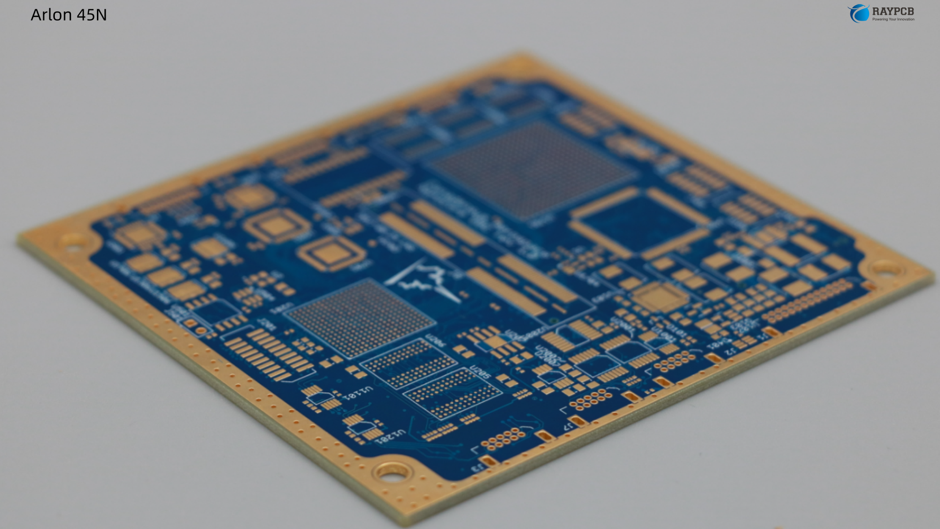
Arlon 45N laminate: full specs (Tg 175°C, Dk 4.2–4.6, Z-expansion 2.4%), prepreg styles, FR-4-compatible processing, and high layer count MLB applications explained.
Before anything else, a clarification that will save you from a specification error that shows up repeatedly across the web: Arlon 45N is not a polyimide. It is a tough, high-Tg multifunctional epoxy laminate and prepreg system. The confusion likely arises because it sits alongside Arlon’s polyimide products in the electronic substrates portfolio, and several third-party sources have mislabeled it. If your design specification calls for a true polyimide resin — full Tg above 250°C, IPC-4101/40 or /41 qualification — you want Arlon 35N or 85N, not 45N. If you need a high-performance, high-Tg epoxy that processes on standard FR-4 lines and handles lead-free assembly reliably, Arlon 45N is exactly the right material.
With that established, let’s dig into what Arlon 45N actually delivers: its chemistry, complete electrical and mechanical properties, available prepreg configurations, detailed process guidelines, and the real-world applications where it outperforms standard difunctional FR-4 without requiring the complexity and cost of polyimide processing.
What Is Arlon 45N?
Arlon 45N is a tough, high glass transition temperature (Tg of 175°C by DSC) multifunctional epoxy laminate and prepreg system designed for use in a variety of higher layer count multilayer boards (MLBs). It is manufactured by Arlon Electronic Materials Division, now part of Rogers Corporation, and meets the requirements of IPC-4101/26 — the slash sheet specification for multifunctional epoxy resin/E-glass laminates.
The “multifunctional” designation in the resin chemistry is the technical distinction from standard FR-4. Standard difunctional epoxy resins use bisphenol-A epoxy resin cured with dicyandiamide (DICY), achieving Tg values in the 130–145°C range. Multifunctional epoxy systems incorporate epoxy resins with higher functionality — typically tetrafunctional or novolac-based components — which create a denser, more crosslinked polymer network upon curing. That denser crosslink density is what pushes the Tg to 175°C and simultaneously delivers better resistance to thermal-induced defects like barrel cracking, inner layer copper cracking, and measling.
Critically, Arlon 45N processes using conventional FR-4 conditions. This is not a trivial feature — it means your existing lamination press, drill programs, etch chemistry, and plating processes work without modification. You’re upgrading the material performance, not the production line.
For engineers working with Arlon PCB materials and evaluating the substrate spectrum from standard FR-4 to high-reliability polyimide, Arlon 45N occupies a clearly defined middle tier: meaningfully better than standard FR-4 in every thermal and reliability metric, significantly lower cost and complexity than polyimide, and fully compatible with the FR-4 process flow that most PCB fabrication shops already run.
Arlon 45N Key Features and Compliance
Understanding what Arlon 45N is qualified to and what it’s specifically engineered to resist is the starting point for any design justification conversation.
| Feature | Detail |
| IPC Qualification | IPC-4101/26 (description and specification) |
| Resin Type | Multifunctional epoxy |
| Tg (DSC) | 175°C |
| Flammability | UL-94 V-0 |
| Lead-Free Compatibility | Yes — suitable for most lead-free applications |
| RoHS/WEEE Compliance | Fully compliant |
| Barrel Cracking Resistance | Specifically engineered |
| Inner Layer Copper Cracking Resistance | Specifically engineered |
| Measling Resistance | Yes |
| Solder Shock Resistance | Yes |
| Processing Compatibility | Conventional FR-4 conditions |
The resistance to barrel cracking and inner layer copper cracking is worth calling out because these are the failure modes that plague standard FR-4 in higher layer count builds. As board thickness and layer count increase, the Z-axis expansion during soldering generates larger absolute displacement in through-hole barrels. Standard FR-4 with lower Tg expands more aggressively above its glass transition point, and the barrel-to-copper interface cracks under that repeated stress. Arlon 45N’s higher Tg keeps the resin in its glassy, lower-expansion state through more of the thermal excursion, reducing the strain on hole barrels directly.
Measling — the formation of white spots or crosses beneath the surface of a laminate caused by separation at the weave-resin interface — is a cosmetic defect that also signals incipient laminate degradation. Its presence in a populated board is a quality alert. Arlon 45N’s tougher resin-to-glass adhesion resists measling formation during both thermal and mechanical stress events.
Complete Arlon 45N Electrical Properties
| Electrical Property | Value | Test Method / Condition |
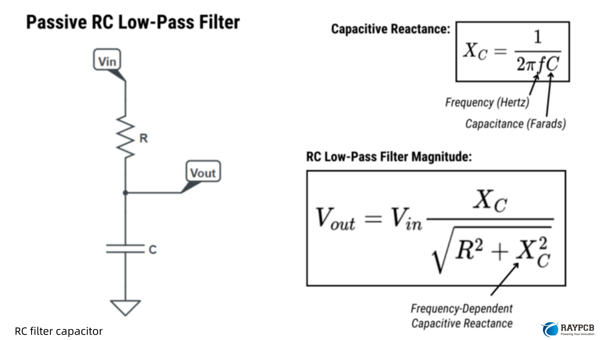
| Dielectric Constant (Dk) @ 1 MHz | 4.2 – 4.6 | IPC TM-650 2.5.5.3 |
| Dissipation Factor (Df) @ 1 MHz | 0.025 | IPC TM-650 2.5.5.3 |
| Volume Resistivity (C96/35/90) | 2.6 × 10⁷ MΩ·cm | IPC TM-650 2.5.17.1 |
| Volume Resistivity (E24/125) | 3.3 × 10⁷ MΩ·cm | IPC TM-650 2.5.17.1 |
| Electrical Strength | 1,500 kV/mm | IPC TM-650 2.5.6.2 |
A Dk of 4.2–4.6 at 1 MHz is typical for an epoxy/E-glass composite, placing Arlon 45N in the same range as standard FR-4. The practical implication is that existing impedance-controlled trace width calculations and stack-up designs do not need significant rework when transitioning from standard FR-4 to Arlon 45N. The Dk shift is minor enough that standard impedance calculation tools will produce consistent results using the same Dk values you’d assign to 180°C-class FR-4.
The Df of 0.025 at 1 MHz is consistent with epoxy-based laminates at that frequency. Engineers designing signal paths above a few gigahertz should note that this dissipation factor will produce measurable insertion loss compared to low-loss thermoset or PTFE alternatives. For the applications Arlon 45N targets — backplanes, high layer count digital boards, automotive electronics — this is not a limiting factor. But if your design pushes into RF or high-speed serial lanes at 25+ Gbps where dielectric loss is a budget constraint, the Arlon 25N or DiClad series materials are better candidates.
Arlon 45N Complete Thermal and Mechanical Properties
This is where Arlon 45N earns its place in the material selection hierarchy over standard FR-4.
Thermal Properties
| Thermal Property | Value | Notes |
| Glass Transition Temperature (Tg) by DSC | 175°C | Primary thermal qualification parameter |
| Decomposition Temperature (Td) at 5% | >300°C | Vs. typical FR-4 at ~300°C |
| Z-Axis Expansion (50°C to 260°C) | 2.4% | Vs. 3.5–5.0% for standard FR-4 |
| CTE X, Y (in-plane) | 14–16 ppm/°C | |
| CTE Z (below Tg) | 55 ppm/°C | |
| CTE Z (above Tg) | 200 ppm/°C | |
| Thermal Conductivity | 0.25 W/mK | ASTM E-1225 |
The Tg of 175°C by DSC is the number most engineers reach for first when evaluating this material, and it bears some context. In lead-free soldering, peak board temperatures during reflow typically reach 245–260°C for brief durations — well above the 175°C Tg. This might seem alarming at first glance, but what matters for solder reflow reliability isn’t how the Tg compares to the solder peak, it’s how the T260 (time-to-delamination at 260°C) compares to actual process exposure times. A higher-Tg laminate like Arlon 45N has better T260 performance than standard FR-4, meaning it survives the thermal exposure of lead-free reflow without delaminating.
The Z-axis expansion of 2.4% from 50°C to 260°C is significantly better than the 3.5–5.0% range typical of standard difunctional FR-4. This directly controls barrel fatigue accumulation in plated-through holes across repeated thermal excursions during assembly, rework, and field thermal cycling.
Mechanical Properties
| Mechanical Property | Value | Notes |
| Peel Strength (after thermal stress) | 8 N/mm | IPC TM-650 2.4.8 |
| Peel Strength (at elevated temperature) | 8 N/mm | IPC TM-650 2.4.8.2 |
| Peel Strength (after process solutions) | 8 N/mm | IPC TM-650 2.4.8 |
| Young’s Modulus (CD/MD) | 2.8 Mpsi | |
| Poisson’s Ratio | 0.2 | |
| Water Absorption | 0.1% | |
| Density | ~1.85 g/cm³ | ASTM D792 |
The uniform peel strength of 8 N/mm under thermal stress, elevated temperature, and after process solutions indicates consistent copper adhesion through all fabrication stages — a key quality parameter for high-layer-count builds where inner layer delamination during lamination is a real failure risk.
Water absorption of 0.1% is low for an epoxy-based material and contributes to Arlon 45N’s dimensional stability and long-term electrical reliability in humid environments. Lower moisture uptake means less shift in Dk and Df in humid operating conditions, and less risk of steam-induced blistering during soldering if pre-bake discipline is maintained.
Arlon 45N Prepreg Availability by Glass Style
Arlon 45N is available in both copper-clad laminate form and B-stage prepreg, making it suitable for single-sided, double-sided, and complex multilayer constructions. The prepreg is available across a range of standard glass fabric styles.
| Glass Style | Typical Resin % | Scaled Flow Hf (mils) | Scaled Flow ΔH (mils) |
| 106 | 72 ± 3 | 1.7 ± 0.3 | 0.75 ± 0.20 |
| 1080 | 63 ± 3 | 2.4 ± 0.3 | 0.75 ± 0.20 |
| 2313 | 55 ± 3 | 3.4 ± 0.3 | 0.75 ± 0.20 |
| 2116 | 50 ± 3 | 4.1 ± 0.3 | 0.75 ± 0.20 |
| 7628 | 40 ± 3 | 6.6 ± 0.3 | 0.70 ± 0.20 |
The 7628 style is the standard workhorse for bulk dielectric thickness in multilayer stackups. The 106 and 1080 styles provide thin bondline options for controlled impedance stackups where precise dielectric spacing between layers is critical. The tight ΔH values (scaled flow tolerance) of ±0.20 mils support predictable and repeatable finished dielectric thicknesses after lamination, which is critical for consistent impedance control across production lots.
For high layer count boards — which is precisely where Arlon 45N is most frequently specified — prepreg consistency across glass styles is an important manufacturing quality factor. Variable dielectric thickness between cores means variable impedance and potentially failed electrical test results that require rework or scrap.
Standard Laminate Thickness Options
Arlon 45N copper-clad laminates are available in a range of standard dielectric thicknesses. When ordering, specify copper weight (typically 1/2 oz, 1 oz, or 2 oz HTE electrodeposited copper), core thickness, and any special requirements.
| Nominal Thickness (inches) | Typical Use |
| 0.004 – 0.010 | Thin cores for high layer count MLB inner layers |
| 0.010 – 0.020 | General-purpose multilayer cores |
| 0.020 – 0.040 | Signal/power layer pairs in thicker constructions |
| 0.040 – 0.062 | Double-sided and outer layer cores |
Contact Arlon customer service for availability confirmation on non-standard thicknesses and special configurations.
Where Arlon 45N Laminate Is Specified: Core Applications
High Layer Count Multilayer PCBs
This is the primary design driver for Arlon 45N. As layer count increases — from 8 layers to 16, 24, or beyond — the thermal stresses on plated-through holes multiply. Each lamination step, each solder reflow pass, and each assembly rework cycle applies cumulative barrel fatigue. Standard FR-4’s higher Z-axis expansion accelerates that fatigue accumulation. Arlon 45N’s 2.4% Z-axis expansion from 50°C to 260°C (versus 3.5–5.0% for standard FR-4) and Tg of 175°C extend the barrel fatigue life meaningfully, making it the sensible material upgrade for any board design that pushes above 12 layers or exceeds 0.093″ finished thickness.
The material’s resistance to inner layer copper cracking is equally important in high layer count constructions. During lamination of thick multilayer stackups, differential expansion between the copper foil and the resin system can crack inner layer copper traces at stress concentration points. Arlon 45N’s tougher resin chemistry is specifically formulated to resist this failure mode.
Backplanes and Motherboards
Server backplanes, data center switching fabrics, and high-density motherboards combine high layer count with large physical dimensions and high-speed serial interfaces. The large board size means that differential thermal expansion across the board area during assembly creates significant in-plane mechanical stress. Arlon 45N’s CTE of 14–16 ppm/°C in the X, Y plane is consistent with copper’s ~17 ppm/°C, reducing in-plane stress at solder joints and pad structures. The higher Tg also ensures that the board retains mechanical stiffness throughout lead-free reflow profiles that would push standard FR-4 into its rubbery regime.
For high-speed digital signals at 10–25 Gbps running across these boards, the Dk of 4.2–4.6 and Df of 0.025 at 1 MHz are acceptable for the moderate trace lengths involved. Engineers targeting 50+ Gbps PAM4 signaling at very long trace runs would look to lower-loss materials, but the bulk of backplane and motherboard traffic sits comfortably within Arlon 45N’s electrical performance envelope.
Ball Grid Array (BGA) Packaging Substrates and Package-on-Package Designs
BGA packages present a specific challenge: the package substrate must survive the thermal shock of solder reflow while maintaining dimensional stability closely matched to the BGA’s copper pad array pitch. Registration errors caused by differential expansion between the board and the component lead to solder joint failures that are often intermittent and difficult to diagnose. Arlon 45N’s controlled CTE and higher Tg support BGA package integration by maintaining consistent expansion behavior during soldering and improving the long-term fatigue resistance of BGA solder joints under operating temperature cycling.
Fine-pitch BGA packages — with ball pitches below 0.5mm — are particularly sensitive to substrate dimensional accuracy. The excellent dimensional stability of Arlon 45N during processing supports the registration accuracy these packages require.
Automotive Under-Hood Electronics
Under-hood automotive electronics — engine management units (ECUs), transmission controllers, ABS modules, and ADAS sensor fusion boards — routinely operate at ambient temperatures of 85°C to 105°C and face transient thermal spikes above 125°C. Standard FR-4 with a Tg of 130–145°C has marginal thermal headroom in this environment, and the coefficient of thermal expansion shifts significantly when the operating temperature approaches Tg. Arlon 45N’s Tg of 175°C provides 50–70°C of additional thermal margin above typical under-hood operating temperatures, keeping the laminate firmly in its glassy, low-expansion regime throughout the vehicle’s operational temperature range.
The material’s solder shock resistance is also relevant here. Automotive assembly processes increasingly use lead-free reflow, and the thermal shock of lead-free HASL and reflow on boards that will subsequently be tested at cold temperatures creates a stress cycle that demands material resilience. Arlon 45N handles this combination reliably.
Lead-Free Assembly Production Boards
Even for products with moderate operating temperature requirements, the lead-free assembly process itself justifies Arlon 45N over standard FR-4 in some production environments. Multiple reflow passes, automated optical inspection (AOI) oven exposure, rework operations, and ICT fixture thermal cycling all contribute to cumulative thermal stress on the laminate. Arlon 45N’s suitability for most lead-free applications, combined with its better T260 performance, makes it a lower-risk material for lead-free production with multiple thermal excursions.
Military and Defense Digital Electronics
While Arlon’s polyimide materials (35N, 85N) handle the most demanding aerospace and defense thermal environments, many military digital electronics applications operate in temperature ranges where 175°C Tg is entirely adequate — particularly in avionics computing units, communications systems, and ground vehicle electronics that operate in controlled compartments. For these applications, Arlon 45N offers the reliability benefits of a higher-Tg material with the lower cost and conventional processability that high-volume military production requires.
How Arlon 45N Compares to Related Materials
Material selection never happens in isolation. Here’s a practical comparison of Arlon 45N against the materials engineers most often evaluate alongside it.
| Property | Standard FR-4 | Arlon 45N | Arlon 35N | Arlon 85N |
| Resin Type | Difunctional epoxy | Multifunctional epoxy | Pure polyimide | Pure polyimide |
| Tg (DSC, °C) | 130–145 | 175 | >250 | >250 |
| Td at 5% (°C) | ~300 | >300 | 407 | >400 |
| Z-Axis Expansion 50–260°C | 3.5–5.0% | 2.4% | 1.2% | ~1.2% |
| CTE Z below Tg (ppm/°C) | 60–70 | 55 | 51 | ~50 |
| Dk @ 1 MHz | 4.2–4.8 | 4.2–4.6 | 4.2 | ~4.2 |
| Df @ 1 MHz | ~0.020–0.025 | 0.025 | 0.010 | ~0.010 |
| Water Absorption | 0.15–0.25% | 0.10% | 0.26% | ~0.25% |
| Flammability | V-0 | V-0 | V-1 | V-0 |
| IPC-4101 Slash Sheet | /21 or /24 | /26 | /40, /41 | /40, /41, /42 |
| Processing | Standard FR-4 | Standard FR-4 | Modified polyimide | Modified polyimide |
| Relative Material Cost | Baseline | 2–3× FR-4 | 4–6× FR-4 | 5–8× FR-4 |
Arlon 45N’s position is clear: it bridges standard FR-4 and polyimide without requiring the specialized lamination equipment, extended cure cycles, or desmear chemistry modifications that polyimide processing demands. For many high-reliability commercial and industrial applications, 45N is the most cost-effective choice that still meets the thermal and mechanical reliability bar.
Arlon 45N Fabrication Process Guidelines
Inner Layer Preparation
Process inner layers through develop, etch, and strip using standard industry practices. Use brown oxide on inner layers and adjust dwell time in the oxide bath to ensure uniform coating. Bake inner layers in a rack for 60 minutes at 107°C–121°C (225°F–250°F) immediately prior to lay-up.
Prepreg Storage and Conditioning
Vacuum desiccate the prepreg for 8–12 hours prior to lamination. Prepreg storage should be in a controlled environment — cool temperatures and low relative humidity — to minimize moisture uptake before lamination. Even with Arlon 45N’s low water absorption of 0.1%, proper prepreg conditioning is good practice that protects laminate quality and bond integrity.
Lamination Cycle
| Step | Parameter |
| Pre-vacuum | 30 minutes |
| Heat rise rate | 8–12°F (4.5–6.5°C) per minute between 210°F and 300°F (100°C and 150°C) |
| Cure start temperature | 360°F (180°C) |
| Cure time | 90 minutes at temperature |
| Cool down | Under pressure at ≤12°F/min (6°C/min) |
Lamination pressures depend on panel size and are consistent with standard FR-4 multilayer practice:
| Panel Size (inches) | Pressure (psi) | Pressure/29″ (psi) | Vacuum (psi) |
| 12 × 18 | 275 | 200 | — |
| 16 × 18 | 350 | 250 | — |
| 18 × 24 | 400 | 300 | — |
Drilling
Standard FR-4 drilling parameters apply. Drill at 350 SFM. Undercut bits are recommended for vias 0.018″ (0.45mm) and smaller. The multifunctional epoxy resin is tougher than standard FR-4, so monitor drill wear and replace tooling on schedule to maintain hole wall quality in dense via patterns.
Desmear
Use alkaline permanganate or plasma desmear. Slightly longer dwell times may be needed for multifunctional compared with difunctional FR-4, but the process chemistry itself is standard and no exotic equipment is required. This is one of the important processability advantages Arlon 45N holds over polyimide-based laminates, where specialized permanganate parameters or plasma desmear is mandatory.
Pre-Assembly Bake
Bake boards for 1–2 hours at 121°C (250°F) before solder reflow or HASL. Even though Arlon 45N’s water absorption of 0.1% is low, moisture absorbed during storage or post-fabrication handling can cause blistering during the thermal shock of lead-free soldering. This bake is standard best practice for any high-reliability multilayer board, regardless of laminate type.
Useful Resources for Arlon 45N Engineers
| Resource | Description | Link |
| Arlon 45N Official Product Page | Product overview, features, IPC qualification | arlonemd.com |
| Arlon 45N Datasheet (Official PDF) | Full properties table, prepreg availability, lamination cycle | arlonemd.com (PDF) |
| MatWeb: Arlon 45N Material Entry | Searchable mechanical/electrical properties database with unit conversions | matweb.com |
| UL Prospector: Arlon 45N | Material properties with UL data (free registration required) | ulprospector.com |
| Arlon “Everything You Wanted to Know” Laminate Guide | Deep technical reference on Tg, Td, CTE, PTH reliability, and material selection | arlonemd.com (PDF) |
| IPC-4101 Specification | Industry base standard for rigid PCB laminates; 45N qualifies to /26 slash sheet | ipc.org |
| Arlon Electronic Substrates Portfolio Overview | Side-by-side product listing covering 33N, 35N, 37N, 38N, 44N, 45N, 47N, 51N, 85N | arlonemd.com |
| PCBSync Arlon Materials Guide | Independent comparison of Arlon material grades with application guidance | pcbsync.com |
Frequently Asked Questions About Arlon 45N
1. Is Arlon 45N a polyimide material?
No. Arlon 45N is a multifunctional epoxy laminate and prepreg system. It is frequently mislabeled as polyimide in informal sources, but the Arlon datasheet and IPC-4101/26 qualification are unambiguous: this is an epoxy-based material. Arlon’s true polyimide products are the 33N, 35N, and 85N series. If you need IPC-4101/40 or /41 polyimide qualification, or a Tg above 200°C, Arlon 45N is not the correct selection. For Tg 175°C, FR-4-compatible processing, UL94-V0, and lead-free compatibility in high layer count multilayer boards, Arlon 45N is the right choice.
2. Can Arlon 45N be processed on existing FR-4 fabrication lines without process requalification?
Essentially yes — this is one of Arlon 45N’s primary value propositions. The lamination cycle uses standard FR-4 temperatures (cure at 180°C/360°F versus 170–175°C for standard FR-4 — a modest increase), conventional desmear chemistry, standard drill parameters, and standard plating processes. The main adjustments are slightly extended permanganate desmear dwell times compared to difunctional FR-4, and a pre-assembly bake before soldering. No specialized press equipment, no plasma-only desmear requirement, no sodium etch treatment. Most fabrication shops experienced with any high-Tg epoxy product will find Arlon 45N a straightforward production introduction.
3. What is the T260 performance of Arlon 45N, and does it support lead-free soldering?
Arlon 45N is explicitly described as suitable for most lead-free applications. The Tg of 175°C combined with the multifunctional crosslink density gives it meaningfully better T260 performance than standard difunctional FR-4 (Tg 130–145°C). While the Arlon 45N datasheet does not publish a T260 value in the same format as the polyimide series (which publish T260 >60 minutes), the material’s design intent for lead-free compatibility is confirmed by Arlon. For boards that will see multiple reflow passes, rework, or any assembly sequence with more than two complete reflow profiles, confirm specific T260 data with Arlon’s applications engineering team.
4. How does Arlon 45N differ from Arlon 47N, and which should I specify for a controlled impedance backplane?
Both 45N and 47N are multifunctional epoxy systems in Arlon’s electronic substrate portfolio. Arlon 47N is specifically a low-flow tetrafunctional epoxy prepreg. The “low-flow” characteristic means it has been formulated to limit resin flow during lamination, which is beneficial in multilayer constructions with fine inner layer features, blind vias, or controlled-depth routing where excessive resin bleed would fill features undesirably. If you have a straightforward high layer count multilayer without flow-critical features, Arlon 45N is the standard choice. If your design includes filled vias, tightly spaced features, or sequential lamination steps where resin flow control is critical, evaluate Arlon 47N alongside 45N. For controlled impedance backplanes without flow-critical features, Arlon 45N is typically the preferred material.
5. What failure modes does Arlon 45N specifically address compared to standard FR-4?
Arlon 45N is engineered to address four specific failure mechanisms that appear in high layer count and thermally demanding FR-4 builds. First, barrel cracking in plated-through holes, caused by the Z-axis expansion differential between copper and the resin during thermal cycling — the higher Tg and lower Z-axis expansion of 45N directly reduce the stress driving this failure. Second, inner layer copper cracking at stress concentrators during lamination of thick multilayer packs — the tougher resin chemistry resists the fracture events that crack inner layer copper traces. Third, measling (resin-glass interface separation visible as white spots) under thermal and mechanical stress — the improved resin-to-glass bond strength in 45N resists measle formation. Fourth, solder shock delamination during lead-free assembly — the higher Tg and T260 performance prevent the catastrophic delamination events that occur when standard FR-4 is pushed through lead-free reflow profiles close to or above its glass transition temperature.
Summary
Arlon 45N is a tough, high-Tg (175°C by DSC) multifunctional epoxy laminate and prepreg system built for high layer count multilayer PCBs, BGA packaging, automotive under-hood electronics, backplanes, and any application where standard difunctional FR-4’s thermal and mechanical limitations create reliability risk. It processes on conventional FR-4 fabrication lines with modest adjustments, carries UL-94 V-0 and IPC-4101/26 qualifications, is fully RoHS compliant, and supports lead-free assembly.
For PCB engineers navigating the performance gap between standard FR-4 and full polyimide, Arlon 45N delivers a well-defined value proposition: significantly better Z-axis expansion control (2.4% vs. 3.5–5.0% for standard FR-4), 30–45°C higher Tg, specific resistance to the barrel cracking and copper cracking failure modes that dominate high layer count reliability failures, and all of this without requiring a new production line qualification or specialized fabrication equipment. It is a practical, cost-effective upgrade that has earned a long track record in demanding commercial, industrial, and automotive applications.
All property values listed are typical values from official Arlon documentation and should not be used as specification limits. Properties may vary depending on design and application. Verify all data against the current Arlon 45N datasheet before finalizing any design specification.