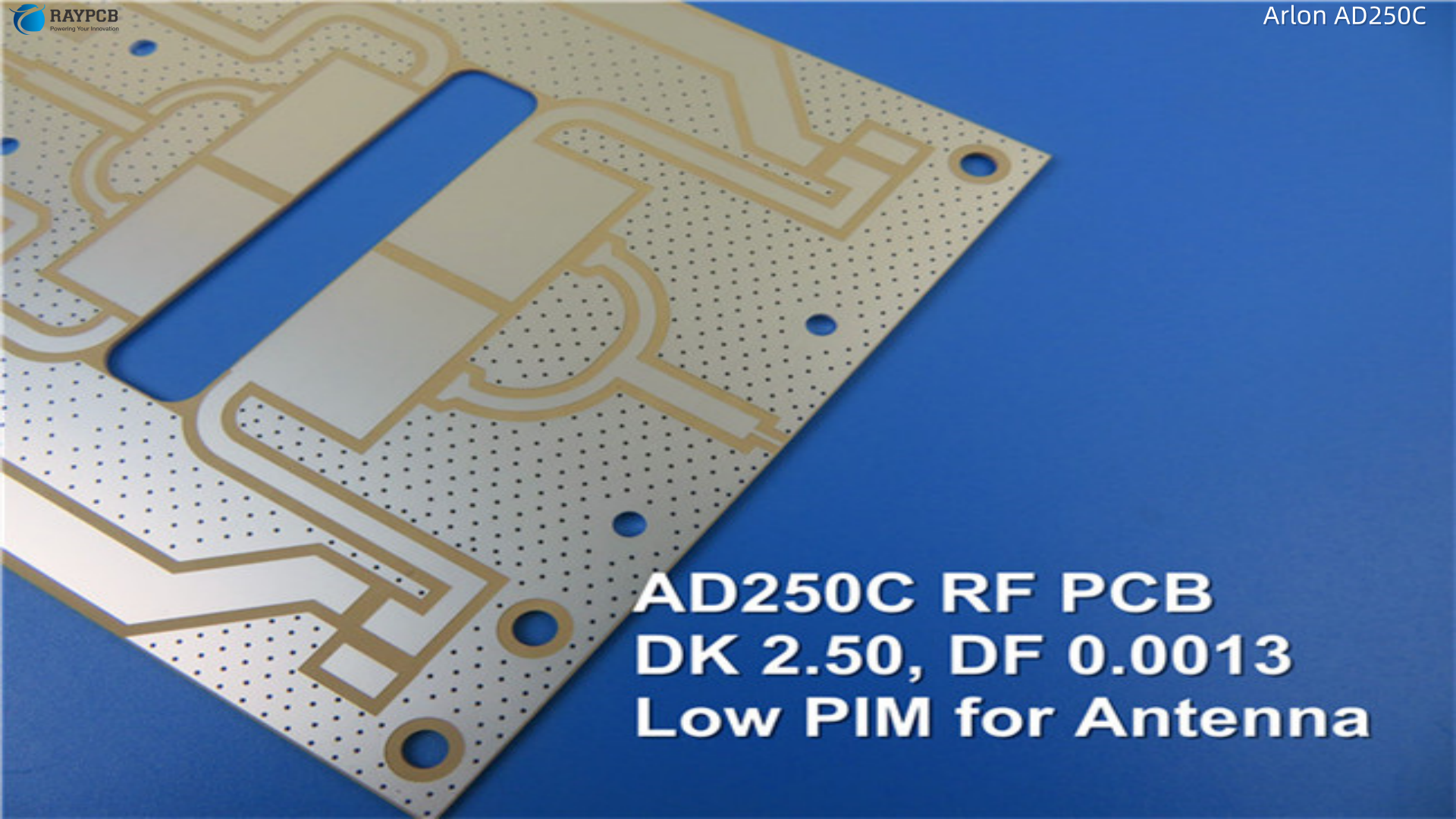
Arlon AD250C Laminate: Datasheet, Properties & PCB Design Guide

Arlon AD250Cย full datasheet review: Dk 2.50, Df 0.0013, PIM performance, CTE values, PCB design tips, and how it compares to RO4350B and the full AD Series.

If you have spent any time designing RF front-ends, base station antenna feed networks, or microwave circuits above 5 GHz, you have almost certainly encountered Arlon AD250C โ€” or been told you should be using it. It sits in a specific, well-defined space in the high-frequency laminate market: low dielectric constant, ultralow loss, excellent PIM performance, reasonably processable with standard PTFE-based PCB workflows, and cost-competitive compared to pure PTFE alternatives.

This guide covers everything a PCB engineer needs to know about AD250C: the complete electrical, thermal, and mechanical property set drawn directly from the Rogers/Arlon datasheet, how it compares to the rest of the AD Series family and to competing materials, the specific design guidelines that differentiate PTFE-based laminate work from standard FR-4 practice, and the applications it is genuinely suited for versus where other materials make more sense.

What Is Arlon AD250C? Background and Material Architecture

Arlon AD250C is a third-generation commercial microwave laminate from Rogers Corporation (which acquired Arlon Electronic Materials in 2014). The AD designation stands for Antenna Dielectric, which accurately describes the product’s primary target: antenna systems for wireless infrastructure, particularly base station antennas operating across the cellular frequency bands from 700 MHz through 5 GHz and beyond.

The AD Series antenna materials are glass-reinforced, PTFE-based materials that provide controlled dielectric constant, low loss performance, and very good passive intermodulation (PIM) performance. The woven glass reinforcement affords good circuit processability and enables high yield circuit board fabrication.

The material architecture of AD250C combines three key constituents: a polytetrafluoroethylene (PTFE) fluoropolymer resin matrix, woven fiberglass reinforcement, and microdispersed ceramic filler. The PTFE resin provides the fundamental low-loss electrical properties. The woven glass reinforcement gives the laminate mechanical stiffness, dimensional stability, and processability advantages over unreinforced PTFE. The ceramic filler is the key differentiation from earlier PTFE/glass composites โ€” the inclusion of differential dispersion ceramics enhances thermal stability, offering lower coefficients of thermal expansion and higher phase stability at elevated temperatures.

The AD250C variant also marks a significant improvement over previous generations in terms of cost efficiency. This combination โ€” low loss, dimensional stability, thermal performance, and cost-efficiency โ€” is what pushed AD250C into volume production use for cellular infrastructure.

Arlon AD250C Datasheet: Complete Electrical Properties

The following property values are drawn from the official Rogers Corporation AD Series datasheet (Publication #92-197, revised 2023). All values are typical values measured on standard test specimens unless otherwise noted.

Dielectric Constant (Dk)

Measurement MethodAD250C ValueTest Conditions
Process Dk2.5223ยฐC @ 50% RH, 10 GHz, IPC TM-650 2.5.5.5
Design Dk2.50C-24/23/50, 10 GHz, Microstrip Differential Phase Length

The distinction between process Dk (2.52) and design Dk (2.50) is important for circuit engineers. The controlled dielectric constant (ยฑ0.05) enables repeatable circuit performance. Process Dk is the value measured by the standard IPC method and represents how the material is characterized in production. Design Dk is the value you use when modeling transmission lines in your electromagnetic simulation tool โ€” it accounts for how copper foil roughness and the differential phase length method interact with the bulk material measurement. Always use the design Dk of 2.50 when calculating microstrip and stripline dimensions.

The very low Dk of 2.50 has a direct consequence for trace geometry: microstrip lines on AD250C are wider than equivalent 50-ohm lines on higher-Dk materials like Rogers RO4350B (Dk 3.48) or standard FR-4 (Dk ~4.3). Wider traces mean lower current density and lower conductor loss for the same impedance โ€” a genuine advantage for high-power antenna applications.

Dissipation Factor (Df) โ€” Loss Tangent

The AD Series antenna products have very low loss (typically less than 0.002 at 10 GHz). The precise AD250C dissipation factor is 0.0013 at 10 GHz, measured at 23ยฐC and 50% RH using IPC TM-650 2.5.5.5.

At 0.0013, AD250C ranks among the lowest-loss commercial microwave laminates available. Pure PTFE materials can reach 0.0009โ€“0.0010, but at significantly higher cost and with more demanding processing requirements. The ceramic-loaded PTFE/glass architecture of AD250C achieves a practical compromise between loss performance and manufacturing yield.

The thermal coefficient of dielectric constant is โˆ’117 ppm/ยฐC over the 0 to 100ยฐC range. This negative value means Dk decreases slightly as temperature rises, which affects phase velocity of signals in the board โ€” a consideration for phase-critical circuits like antenna feed networks with tight beam-steering requirements over temperature.

PIM Performance

Passive Intermodulation (PIM) is the dominant specification driver for base station antenna materials. PIM performance for AD250C is โˆ’159/โˆ’163 dBc at reflected 43 dBm swept tones at 1900 MHz, using S1 foil measured at 0.030″ and 0.060″ thicknesses respectively.

PIM is generated by nonlinear mechanisms at copper surfaces, connections, and the dielectric itself. The PTFE matrix in AD250C contributes minimal PIM from the dielectric side. However, PIM performance is heavily influenced by the copper choice. Reverse-treated electrodeposited (ED) copper, which Rogers designates S1 foil, minimizes the surface micro-roughness that is one of the primary PIM generation mechanisms in PTFE-based boards. Standard ED copper will give measurably worse PIM, so the copper foil selection must be aligned with the PIM requirement of the specific application.

Additional Electrical Properties

PropertyAD250C ValueUnitsTest Conditions
Volume Resistivity4.8 ร— 10โธMฮฉ-cmC96/35/90
Surface Resistivity4.1 ร— 10โทMฮฉC96/35/90
Dielectric Strength979V/milIPC TM-650 2.5.6.2
Dielectric Breakdown>40kVD-48/50, X/Y direction

Arlon AD250C Thermal Properties

Thermal performance is the second defining characteristic of AD250C, and it is where the ceramic filler contribution becomes numerically obvious.

Coefficient of Thermal Expansion (CTE)

CTE AxisAD250C ValueUnitsTemperature Range
X-axis CTE47ppm/ยฐCโˆ’55ยฐC to 288ยฐC
Y-axis CTE29ppm/ยฐCโˆ’55ยฐC to 288ยฐC
Z-axis CTE196ppm/ยฐCโˆ’55ยฐC to 288ยฐC

The Z-axis CTE of 196 ppm/ยฐC is the primary reliability parameter for plated through-hole (PTH) via reliability. Pure PTFE materials have Z-axis CTE values in the range of 200โ€“400 ppm/ยฐC, which is why reliability of PTH vias in thick PTFE boards has historically been poor. The low z-axis thermal expansion improves the reliability of plated through-hole (PTH) connections compared to typical PTFE base materials. Low X-Y expansion improves the reliability of BGA solder joints. At 196 ppm/ยฐC, AD250C still requires careful design of via aspect ratios and use of copper-filled via plugging in demanding thermal cycling environments, but it represents a meaningful improvement over unfilled PTFE.

Note the asymmetry between X-axis (47 ppm/ยฐC) and Y-axis (29 ppm/ยฐC) CTE. This reflects the anisotropy of the woven glass reinforcement โ€” the glass fibers constrain expansion differently in the machine direction versus the cross-machine direction. This asymmetry must be accounted for in precision antenna designs where dimensional stability over temperature affects beam direction accuracy.

Other Thermal Properties

PropertyAD250C ValueUnitsTest Method
Decomposition Temperature (Td)>500ยฐCIPC TM-650 2.3.40 (5% weight loss)
Time to Delamination (T-288)>60minutesIPC TM-650 2.4.24.1
Thermal Conductivity0.33W/(mยทK)ASTM D5470, Z-direction
Specific Heat Capacity0.813J/gยทKASTM E2716

The decomposition temperature above 500ยฐC is exceptional โ€” it means the material survives any realistic PCB processing temperature, including lead-free solder processes that briefly reach 260ยฐC peak reflow temperature and the 288ยฐC T-288 solder float test with time-to-delamination exceeding 60 minutes. This high thermal stability is a direct consequence of the PTFE base resin, which is chemically and thermally inert well above any PCB processing condition.

Arlon AD250C Mechanical and Physical Properties

PropertyAD250C ValueUnitsConditions
Copper Peel Strength2.6 N/mm (14.8 lbs/in)N/mm10s @ 288ยฐC, 35ยตm foil
Flexural Strength (MD/CMD)60.7/44.1 MPaMPa25ยฐC
Tensile Strength (MD/CMD)41.4/38.6 MPaMPa23ยฐC @ 50% RH
Flex Modulus (MD/CMD)6,102/5,364 MPaMPa25ยฐC
Dimensional Stability (MD/CMD)0.02/0.06mils/inchAfter etch + bake
Moisture Absorption0.04%IPC TM-650 2.6.2.1
Density2.28g/cmยณASTM D792
FlammabilityV-0โ€”UL 94

The moisture absorption of 0.04% is critically important for RF performance. The AD Series antenna products have very low moisture absorption (less than 0.1%). Water has a dielectric constant of approximately 80, and any water absorbed into the laminate raises the effective Dk of the substrate. For a 50-ohm transmission line tuned to a target impedance at room temperature and standard humidity, significant moisture uptake would shift the actual impedance and introduce additional loss. At 0.04%, AD250C is among the driest commercial laminates available, which is why it performs consistently in the outdoor, weathering-exposed environments typical of base station antenna deployments.

Copper peel strength for AD250C is greater than 10 pli (pounds per linear inch), with typical values of 14.8 lbs/in measured on 35ยตm foil after 10 seconds at 288ยฐC. Maintaining peel strength after high-temperature excursions is important for antenna panels that undergo soldering and field temperature cycling.

Standard Thicknesses and Panel Sizes

AD250C is available in standard thicknesses of 0.020″ (0.508 mm), 0.030″ (0.762 mm), and 0.060″ (1.524 mm), with thickness tolerances of ยฑ0.002″ for the thinner options and ยฑ0.003″ for the 0.060″ thickness.

The three standard AD250C thicknesses correspond to specific applications in antenna design. The 0.030″ thickness is the most commonly used for single-layer microstrip antenna feed networks. The 0.020″ thickness allows more compact designs where trace width must be minimized. The 0.060″ thickness is used where higher power handling is required, because thicker substrates support wider 50-ohm traces with lower current density and therefore lower IยฒR heating.

Both standard electrodeposited (ED) and reverse-treated ED copper foil options are available. For applications where PIM is a key specification, reverse-treated foil (S1) is the correct selection โ€” the lower surface roughness of the reverse-treated side reduces the micro-contact nonlinearities that drive PIM generation.

AD250C vs. AD255C vs. AD300D vs. AD350A: The Full Series Comparison

AD250C belongs to the AD Series family, and selecting within this family requires understanding how each member is differentiated. All four materials share the same PTFE/ceramic/glass architecture and process compatibility.

PropertyAD250CAD255CAD300DAD350A
Design Dk2.502.602.943.50
Dissipation Factor @ 10 GHz0.00130.00130.00210.0033
Z-axis CTE (ppm/ยฐC)1961969863
Thermal Conductivity (W/mยทK)0.330.350.370.44
Moisture Absorption (%)0.040.030.040.10
PIM @ 1900 MHzโˆ’159/โˆ’163 dBcโˆ’159/โˆ’163 dBcโˆ’159/โˆ’163 dBcโˆ’159/โˆ’163 dBc
Key AdvantageLowest Dk, lowest lossSimilar to AD250C, wider rangeBetter Z-CTE, moderate lossBest Z-CTE, higher Dk
Best Use CaseNarrowband antennas, high-efficiencyPatch antennas, Dk flexibilityMultilayer designs, via reliabilityHigh-reliability multilayer stacks

The choice between AD250C and AD255C often comes down to Dk value, as both have identical dissipation factors. AD255C at Dk 2.60 enables slightly different trace geometries and is often preferred for patch antennas where the substrate thickness and Dk together set the resonant cavity. AD300D and AD350A offer significantly better Z-axis CTE (98 ppm/ยฐC and 63 ppm/ยฐC respectively), making them more appropriate for multilayer designs with many through-hole connections that must survive aggressive thermal cycling.

Arlon AD250C vs. Competing Materials

For engineers evaluating AD250C against alternative laminates, the following comparison covers the most commonly considered substitutes:

MaterialManufacturerDesign DkDf @ 10 GHzZ-CTE (ppm/ยฐC)Key Trade-off vs. AD250C
AD250CRogers (Arlon)2.500.0013196Baseline
RO3003Rogers3.000.0010250Lower Dk not available; lower Df but higher Z-CTE
RO4350BRogers3.480.0037187Higher Dk, much higher Df; better PTH reliability
CLTE-XTRogers (Arlon)2.940.001238Similar Df; excellent Z-CTE; higher cost
XT/duroid 5880Rogers2.200.0009237Lower Dk and Df but more costly, softer
Taconic RF-35Taconic3.500.0018183Higher Dk; less suitable for narrowband
Isola IS680Isola3.260.0020190Higher Dk; FR-4-like processability

AD250C’s primary competitive position is the combination of Dk = 2.50 and Df = 0.0013 at a cost point lower than pure PTFE materials like RT/duroid 5880. For base station antenna applications where the design Dk of ~2.5 is specifically required to achieve the necessary trace widths and phase relationships, AD250C is the default choice in commercial designs.

PCB Design Guidelines for Arlon AD250C

Designing with AD250C differs meaningfully from designing with FR-4 or even standard glass-epoxy hydrocarbon laminates. Engineers working with PTFE-based boards for the first time should understand these differences before sending a board to fabrication.

Transmission Line Impedance Calculation

Always use the design Dk of 2.50, not the process Dk of 2.52, when calculating trace widths for 50-ohm or other target impedances. For a 0.030″ (0.762 mm) thick AD250C substrate with 1 oz (35ยตm) copper, a 50-ohm microstrip trace width is approximately 2.2 mm. This is considerably wider than the equivalent trace on RO4350B (~1.6 mm) or FR-4 (~1.3 mm). This wider trace geometry is not a problem โ€” it is a feature, because wider traces have lower conductor loss. Just ensure your footprint library and transmission line models use the correct Dk value.

For capacitors in matching networks and filter designs on AD250C, the low substrate Dk means that parasitic pad capacitance from component footprints is lower than on higher-Dk substrates. This must be accounted for in element value corrections for circuits designed above 1 GHz.

Handling and Dimensional Stability

PTFE-based materials are softer and more dimensically sensitive than FR-4. AD250C benefits from the dimensional stability of the woven glass reinforcement, but the material still requires careful handling to avoid surface contamination and mechanical distortion. The following practices are essential:

Handle AD250C boards with clean cotton or nitrile gloves at all times. Skin oils contaminate the PTFE surface and degrade surface resistivity and potentially introduce PIM. Maintain boards flat during storage โ€” warped PTFE/glass panels are extremely difficult to flatten without controlled heat cycling.

Use dimensionally stable tooling pins and tight-tolerance tooling holes, because the X-Y CTE anisotropy (47 vs. 29 ppm/ยฐC) means the board will expand differently in MD and CMD directions with temperature. For multi-up panel designs with tight registration requirements, this asymmetric expansion must be built into the panelization and artwork compensation.

Drilling and Through-Hole Processing

Standard carbide drill bits suitable for FR-4 can drill AD250C, but ceramic filler in the material accelerates drill wear faster than with pure PTFE or standard epoxy laminates. Use fresh or recently resharpened drill bits, monitor drill wear closely, and do not reuse drill bits from FR-4 runs on AD250C panels without inspection.

Use hard backup and entry materials to minimize burring at hole entry and exit. PTFE’s softness means it does not cleanly shear at hole walls the way harder materials do; without proper backup, via hole quality degrades. Plasma cleaning or permangante hole preparation is recommended to remove PTFE smear from hole walls before electroless copper deposition, since PTFE’s chemical inertness means standard epoxy desmear chemistry is less effective.

PTFE Surface Preparation for Adhesion

The chemical inertness of PTFE that makes it an excellent low-loss dielectric also makes it resistant to standard bonding and solder mask adhesion processes. Sodium naphthalene etch (chemical etching) or reverse sputter (plasma) treatment of exposed PTFE surfaces is required before applying solder mask, bonding plies in a multilayer stack, or applying conformal coating. Without this surface preparation step, adhesion failure of solder mask or bond-ply prepreg is a common yield problem in PTFE PCB fabrication.

Use Rogers proprietary bond-ply materials or compatible prepregs specifically qualified for PTFE multilayer construction when building AD250C into a multilayer stack. Standard FR-4 prepregs are not compatible with PTFE laminate multilayer construction.

Soldering and Assembly

AD250C has excellent thermal stability through lead-free solder reflow profiles, with a T-288 time-to-delamination exceeding 60 minutes and a decomposition temperature above 500ยฐC. The board will not delaminate or blister during standard reflow processing. However, the relatively low flexural stiffness compared to FR-4 means that AD250C boards require adequate support fixturing during pick-and-place and reflow to prevent warpage under thermal gradient during oven processing.

For edge-mount connectors and SMA launches on AD250C boards, minimize the distance between the connector reference ground plane and the signal launch point. Any discontinuity at the connector-to-board transition introduces reflections that degrade return loss at high frequencies. Model the connector launch geometry in your EM simulator using the actual AD250C Dk and thickness before committing to a physical design.

Typical Applications for Arlon AD250C

Typical applications for AD250C include cellular infrastructure base station antennas, automotive telematics antenna systems, and commercial satellite radio antennas.

More specifically, the primary use cases in commercial volume production are:

Base station antenna feed networks: Power dividers, phase-shift networks, and combiner circuits for 4G LTE and 5G NR antenna arrays, where insertion loss, PIM, and dimensional stability under thermal cycling are all primary specifications. The combination of Df = 0.0013 and โˆ’159 dBc PIM makes AD250C the dominant material in this segment.

Distributed antenna system (DAS) components: Passive splitters and couplers in indoor and outdoor DAS installations, where low loss across the 700โ€“2700 MHz band is required.

Patch antennas for GNSS, GPS, and SDARS: Compact microstrip patch antennas where the substrate Dk directly sets the patch resonant dimensions, and where low moisture absorption ensures consistent resonant frequency in outdoor environments.

Commercial radar and point-to-point microwave links: Circuits operating in the 6โ€“18 GHz bands where Df = 0.0013 provides meaningful link budget advantage over higher-loss alternatives.

Digital audio broadcasting (DAB) antenna systems: Broadband antenna components operating in the VHF and UHF bands where PIM performance is important.

Useful Resources for Arlon AD250C Design Work

ResourceTypeWhy It’s Useful
Rogers AD Series Datasheet (PDF)Official datasheetComplete property tables for AD250C, AD255C, AD300D, AD350A
Rogers MWI-2000 Microwave Impedance CalculatorOnline calculatorFree transmission line impedance calculator pre-loaded with Rogers material Dk values including AD250C
Rogers PCB Design Guidelines for RF and Microwave (PDF)Application noteOfficial handling, drilling, plating, and assembly guidelines for Rogers PTFE-based laminates
IPC-2141A: Controlled Impedance Circuit BoardsIndustry standardDesign and fabrication standard for controlled impedance PCBs including transmission line calculations
Murata SimSurfingComponent simulationVerify parasitic effects of SMD components (capacitors, resistors) on AD250C board topology
MatWeb: Arlon AD250C Material DataMaterial databaseCross-referenced material properties for comparison with alternative laminates
Rogers Technology Support HubTechnical supportApplication notes on microwave PCB design, material selection, and processing
Cirexx Arlon AD Series Processing GuideFabrication referenceProcessing and fabrication guidance for Arlon laminate families

FAQs: Arlon AD250C Laminate

Q1: Is Arlon AD250C still available now that Rogers acquired Arlon, and is it the same material?

Yes, AD250C is currently available from Rogers Corporation under the Rogers brand with AD Series designation (Rogers AD250C). The acquisition of Arlon Electronic Materials by Rogers Corporation in 2014 consolidated the product line under Rogers, but the AD Series materials continued in production with the same specifications. The Rogers AD Series datasheet (Publication #92-197, revised October 2023) is the current authoritative document for all typical property values. The chemistry, architecture, and specifications of AD250C are unchanged from the Arlon era. When ordering from fabricators, both “Arlon AD250C” and “Rogers AD250C” refer to the same material.

Q2: Can AD250C be processed with standard FR-4 fabrication equipment?

Partially. AD250C is fully compatible with standard PTFE printed circuit board substrate processes. However, this means PTFE PCB standard processes โ€” not FR-4 processes. Key differences include: PTFE surface preparation (plasma or chemical etch) required before solder mask and bonding; specific bond-ply materials for multilayer construction; adjusted drilling parameters to account for ceramic filler wear on drill bits; and plasma or permanganate hole preparation for PTH plating. FR-4 desmear chemistries and standard epoxy prepregs are not compatible with AD250C multilayer construction. Fabricators experienced with Rogers PTFE materials (RT/duroid, RO3000 series) can process AD250C on their existing PTFE lines.

Q3: What is the difference between the process Dk (2.52) and design Dk (2.50) on the AD250C datasheet?

The process Dk of 2.52 is measured using the standard IPC TM-650 2.5.5.5 clamped stripline method, which is the characterization method used in production to verify the material lot. The design Dk of 2.50 is measured using the microstrip differential phase length method, which more accurately reflects how electromagnetic fields interact with the material in a real printed circuit transmission line โ€” accounting for the influence of copper foil surface roughness and the fringing field distribution in a microstrip geometry. Always use 2.50 when calculating microstrip trace widths and electrical lengths in your simulation tool. Using 2.52 will introduce a small systematic error in your impedance and electrical length calculations.

Q4: How does AD250C perform at 5G millimeter-wave frequencies (28 GHz, 39 GHz)?

The official Rogers AD Series datasheet characterizes properties at 10 GHz. Dielectric constant decreases slightly and dissipation factor increases with frequency for most laminate materials. For PTFE-based materials like AD250C, the increase in Df with frequency is relatively modest compared to filled thermoset materials, but precise Dk and Df values at 28 GHz or 39 GHz require measurements at those specific frequencies. Rogers provides frequency-dependent Dk and Df curves in the Arlon AD Series technical data package (the Cirexx AD Series PDF referenced in the resources section includes frequency sweep data). For 5G mmWave designs above 24 GHz, consider whether the Df = 0.0013 at 10 GHz is representative of your actual operating frequency, and consult the frequency-dependent curves or request measured data at the target frequency from your Rogers distributor.

Q5: Can I use standard FR-4 prepreg to bond AD250C layers in a multilayer PCB?

No. Standard FR-4 prepreg is not compatible with AD250C multilayer laminate construction. The cure temperature and pressure profile for FR-4 prepregs, combined with the chemical incompatibility between epoxy resin and PTFE surfaces, will result in poor adhesion at the bond-ply/core interfaces and risk of delamination in thermal cycling. Rogers provides compatible bond-ply materials for PTFE multilayer construction. For mixed-dielectric constructions that combine AD250C with an FR-4-type material โ€” sometimes used to achieve a hybrid stack with specific impedance or cost targets โ€” consult the Rogers material compatibility application notes and validate the construction with your fabricator before releasing the design.

Summary: Is Arlon AD250C the Right Choice for Your Design?

Arlon AD250C delivers a specific set of properties in a particular cost-performance window: Dk = 2.50, Df = 0.0013, PIM = โˆ’159 dBc, moisture absorption = 0.04%, and full PTFE thermal stability. If your design needs all five of those characteristics simultaneously โ€” and your application is an antenna, microwave filter, power divider, or other RF passive circuit โ€” AD250C is likely the correct material.

If your design needs even lower loss than 0.0013 at the cost of higher price and more demanding processing, look at RT/duroid 5880. If your design needs better PTH via reliability in a thick multilayer stack, look at AD300D or AD350A, which offer substantially lower Z-axis CTE. If your design can tolerate Df = 0.003โ€“0.004 and needs the simpler processing and better via reliability of a hydrocarbon thermoset, RO4350B is the right choice.

AD250C earns its position in volume commercial production because it sits at the intersection of low enough loss for cellular antenna applications, low enough PIM for base station requirements, stable enough dimensionally for outdoor antenna systems, and cheap enough to use in high-volume antenna panels. That is a well-defined design target, and for that target, it remains the industry standard material.

Arlon AD Bondply: The Complete Guide to Bonding High-Frequency PTFE Laminates in Multilayer PCBs

Learn how Arlon AD bondply bonds high-frequency PTFE laminates in multilayer PCBs โ€” grades, stackup design, lamination parameters, and FAQs for RF engineers.

If you’ve ever tried to build a multilayer RF board using PTFE-based laminates, you already know the headache. PTFE doesn’t bond like FR-4. It flows differently, expands differently, and if you try to laminate it using standard epoxy prepreg, you end up with either mismatched dielectric properties or delamination failures down the road. That’s exactly where Arlon AD bondply enters the picture โ€” and for engineers working on base station antennas, phased array radars, or 5G infrastructure boards, understanding this material properly can be the difference between a first-pass success and a very expensive stack of scrap.

This guide covers everything you need to know: what the AD Series actually is, how its bonding plies work, how to select the right grade for your stackup, and practical tips on multilayer lamination processing. Whether you’re designing a hybrid RF/digital board or an all-PTFE microwave structure, let’s dig in.

What Is the Arlon AD Series? Understanding the PTFE Composite Foundation

<invoke name=”places_search”> <invoke name=”web_search”>

The Arlon AD Series is a family of woven fiberglass-reinforced PTFE composite laminates engineered specifically for printed circuit board substrates in high-frequency applications. What makes it unique compared to traditional PTFE-only substrates is the deliberately higher fiberglass-to-PTFE ratio. This design choice trades a small amount of raw electrical performance for a significant improvement in dimensional stability โ€” something that matters enormously when you’re trying to hold tight impedance tolerances across a multilayer panel.

Arlon’s Electronic Materials Division (EMD), based in Rancho Cucamonga, California, has been producing PTFE-based microwave laminates for over 50 years. The AD product line sits within their microwave materials portfolio alongside CuClad, DiClad, CLTE, and AD1000 series materials, covering dielectric constants from roughly 2.17 up to 10.2.

For the AD Series specifically, dielectric constants range from 2.5 to 3.5, available in dielectric thicknesses from 0.015″ to 0.062″, with custom thicker options available on request. The full lineup covers multiple Dk targets suited to different transmission line geometries and frequency bands.

Key Electrical Attributes of the AD Series

The core electrical appeal of the AD Series is the combination of low loss tangent and stable dielectric constant across a broad frequency range โ€” two things that PTFE does exceptionally well compared to FR-4 or standard epoxy laminates.

PropertyTypical ValueTest Method
Dielectric Constant (Dk)2.5 โ€“ 3.5 (grade-dependent)IPC-TM-650 2.5.5.5 / FSR
Loss Tangent (Df)0.0014 โ€“ 0.003IPC-TM-650 2.5.5.5
Z-axis CTELower than standard PTFEIPC-TM-650 2.4.24
Water Absorption< 0.1%IPC-TM-650 2.6.2
Copper Peel StrengthStandard ED / RTF foilIPC-TM-650 2.4.8

These numbers put the AD Series comfortably ahead of FR-4 (Df typically 0.018โ€“0.025) and broadly in line with competitive PTFE/glass materials from Rogers and Taconic โ€” though specific loss tangent values vary significantly between AD grades.

The AD Series Lineup: Choosing the Right Grade

Not all AD grades are the same. Over the years Arlon has expanded and refined the lineup, introducing ceramic-filled variants (designated with the “A” suffix) that offer even better thermal stability and lower loss. Here’s a practical breakdown:

AD Series Grade Comparison

GradeDk (Nominal)Key FeatureBest Use Case
AD2502.50PTFE/glass, cost-optimizedAntenna substrates, combiner boards
AD255A2.55Ceramic + PTFE + glass, very low Df (0.0014)Base station, high-gain antenna
AD260A2.60Ceramic-filled, tight Dk tolerance, FSR testedTelecom infrastructure, feed networks
AD3003.00Standard PTFE/glass, balanced Dk/costStripline, general microwave
AD300A3.00Ceramic-loaded, improved CTE vs AD300Hybrid multilayer stackups
AD320A3.20 ยฑ 0.04Ceramic, stable to 40 GHzmmWave, 5G, radar, medical imaging
AD350A3.50Ceramic-filled, higher DkMiniaturized circuits, filters
AD100010.2Ultra-high Dk ceramic/PTFEMiniaturization, patch antennas

The “A” designation โ€” visible in AD255A, AD260A, AD300A, AD320A โ€” signals the inclusion of micro-dispersed ceramic filler. This makes a real difference in practice. The ceramic loading reduces the coefficient of thermal expansion (CTE) in the Z-axis, bringing it closer to the expansion rate of copper. The result is improved plated through-hole (PTH) reliability, especially important in multilayer assemblies that see thermal cycling during assembly and field use.

Arlon uses the IPC TM-650 2.5.5.6 (FSR) test method on every panel for the ceramic-filled grades to guarantee dielectric constant consistency โ€” not just statistical sampling. For production PCBs where impedance tolerance is held to ยฑ5% or tighter, that per-panel testing matters.

What Is Arlon AD Bondply and Why Does It Exist?

Here’s where many PCB engineers get tripped up. When you build a multilayer board using AD Series cores, you can’t just sandwich them together with standard FR-4 prepreg and call it a day. The mismatch in dielectric properties and CTE between an epoxy prepreg and a PTFE core would undermine your impedance calculations and create a mechanical weak point at the bond interface.

Arlon AD bondply refers to the bonding ply materials โ€” low-density, resin-rich versions of the same PTFE-based material family โ€” used to join AD Series cores in a multilayer stackup. Arlon supplies copper-clad laminates together with bonding plies and prepregs specifically formulated to maintain electrical continuity and mechanical integrity between layers.

The concept parallels what Rogers does with their 2929 bondply for RO3000 and RT/duroid series laminates: rather than using a dissimilar adhesive, you bond like-with-like. A bonding ply derived from the same PTFE composite system will have compatible Dk, Df, CTE, and thermal processing characteristics, preserving signal integrity across layer boundaries.

Three Bonding Methods for PTFE Multilayer PCBs

Understanding Arlon AD bondply requires understanding where it fits in the broader landscape of PTFE bonding approaches. There are fundamentally three methods used in industry:

MethodMaterial UsedAdvantagesLimitations
Thermoplastic bonding filmsFEP, CTFE, or PTFE filmsLowest electrical lossHigh process temperature; not suited for sequential lamination
Thermoset prepreg / bondplyArlon AD bondply, Rogers 2929Sequential lamination capable; higher layer countSlightly higher Df than thermoplastic films
Fusion (direct) bondingNo adhesive โ€” direct PTFE-to-PTFEMaximum electrical uniformityRequires very high pressure (>1000 PSI), specialized press; challenging registration

The AD bondply approach falls into the thermoset/bondply category. It provides a middle path: better electrical properties than an epoxy prepreg, while being far more manufacturable than fusion bonding, which demands specialized induction heating press equipment and rigid process control.

For the majority of commercial wireless infrastructure boards โ€” base station combiners, antenna feed networks, power dividers โ€” the AD bondply approach offers the right compromise of performance, yield, and cost.

Multilayer Stackup Design with Arlon AD Bondply

Hybrid vs. All-PTFE Stackups

One of the most common real-world scenarios is the hybrid stackup: RF/microwave layers using AD Series cores, combined with lower-cost digital or power layers using FR-4 or mid-loss thermoset materials. This is economically attractive but introduces engineering challenges.

The primary concern is CTE mismatch. AD Series laminates, particularly the ceramic-filled “A” grades, have significantly lower CTE than standard FR-4. Under thermal cycling, differential expansion can stress the plated through-holes and cause barrel cracking or pad lifting. The AD bondply layer helps manage this transition, but the designer still needs to:

  • Keep high-frequency signal layers together in the stackup (avoid crossing the PTFE/FR-4 boundary with critical RF signals)
  • Size via drill diameters and aspect ratios conservatively for PTH zones that span both material types
  • Discuss the stackup with the fabricator early โ€” most shops that handle hybrid PTFE boards have proprietary lamination cycles optimized for specific material pairings

All-PTFE Stackup Considerations

For pure AD Series multilayers using AD bondply throughout:

  • The bonding ply is a lower-density version of the core material, allowing it to flow into trace gaps under heat and pressure during lamination
  • A general rule of thumb in the industry: use 5 mil bondply for every 1 oz of inner-layer copper to ensure adequate encapsulation around etched features
  • Lamination pressure requirements are higher than standard FR-4 โ€” typically exceeding 1000 PSI โ€” and dwell time must be controlled carefully to bring the bondply to full cure without thermal overshoot
  • PinLess lamination methods, commonly used for FR-4 multilayers, are problematic with PTFE because the standard spot-welding step requires very high local temperature and pressure that most welding machines can’t reliably deliver to PTFE. Pinned tooling or specialized induction welding equipment is typically required

Sample AD-Series Hybrid Stackup

LayerMaterialRole
L1AD260A (0.020″)RF signal layer โ€” microstrip
BondAD bondplyInter-layer adhesive
L2โ€“L3AD260A (0.031″)Ground / power plane
BondAD bondplyInter-layer adhesive
L4AD260A (0.020″)RF signal layer โ€” stripline
TransitionLow-flow thermoset prepregCTE buffer toward FR-4
L5โ€“L8High-Tg FR-4Digital / control layers

The key principle: keep RF signal layers grouped within the AD Series zone, and use a controlled-flow transition prepreg when moving to the FR-4 region.

Processing Guidelines for Arlon AD Bondply

If you’re working with a contract manufacturer, making sure they have hands-on experience with PTFE-based multilayers is non-negotiable. Here are the main process parameters to confirm:

Inner Layer Preparation

PTFE-based laminates require a sodium naphthalene (sodium etch) or similar chemical treatment, or a plasma activation process, on the bond surfaces before lamination. Standard oxide or micro-etch surface treatments used for FR-4 are insufficient โ€” they won’t provide adequate adhesion to the bondply. Skipping this step is a common root cause of delamination failures in the field.

Lamination Cycle

Typical parameters for AD bondply lamination (confirm with Arlon’s process guidelines for your specific grade):

ParameterTypical Range
Pressure800 โ€“ 1200 PSI
Peak Temperature350ยฐC โ€“ 380ยฐC (for PTFE-based bondply)
Vacuum Level< 10 mbar
Temperature Ramp Rate2โ€“5ยฐC/min to cure zone
Dwell Time at Peak30โ€“60 min

Note that these cycles are substantially more aggressive than standard FR-4 lamination (typically 175โ€“185ยฐC, 300โ€“500 PSI). Make sure your press, caul plates, and tooling are rated for these conditions.

Drilling and Through-Hole Plating

PTFE is soft and gummy compared to FR-4. Dull drill bits will smear PTFE into the hole wall, creating a contaminated surface that resists copper adhesion in the plating step. Use sharp, fresh drill bits, reduce drill speed or feed rate per the laminate manufacturer’s guidelines, and consider plasma de-smear rather than permanganic de-smear for PTFE-rich stackups.

Applications: Where Arlon AD Bondply Earns Its Keep

Engineers reach for Arlon AD bondply when the application demands both high-frequency electrical performance and the structural integrity of a multilayer PCB. Typical use cases include:

  • 5G base station antennas and feed networksย โ€” where low insertion loss and tight impedance control at 28 GHz and above are critical
  • Phased array radar systemsย โ€” where phase consistency across dozens of parallel signal paths demands a substrate with stable, predictable Dk over temperature
  • Satellite communication transpondersย โ€” operating at Ka-band and higher, where every 0.1 dB of loss matters
  • Medical imaging systemsย (MRI, ultrasound electronics) โ€” high-frequency signal integrity combined with reliability requirements
  • Power amplifier boardsย for wireless infrastructure โ€” where both RF performance and thermal management (enhanced by the ceramic filler’s higher thermal conductivity) are needed simultaneously

For Arlon PCB fabrication services that can handle these demanding stackups, partnering with a manufacturer who stocks Arlon materials and has established process qualification is strongly recommended.

Arlon AD Series vs. Competitive Materials

For context, here’s how the AD Series positions against other commonly specified high-frequency substrates:

MaterialDkDf (@10 GHz)CTE Z-axisProcessability
Arlon AD260A2.60~0.002Low (ceramic-loaded)Standard PTFE process
Arlon AD320A3.200.0032Low (ceramic-loaded)Standard PTFE process
Rogers RT/duroid 58802.200.0009ModerateRequires careful handling
Rogers RO4350B3.480.0037LowNear FR-4 processability
Taconic TLY-52.170.0009ModeratePTFE standard process
Standard FR-44.2โ€“4.80.018โ€“0.025HighEasiest, lowest cost

The AD Series “A” grades occupy a compelling middle ground: better loss performance than RO4350B (which is a thermoset, not PTFE), and far better dimensional stability and PTH reliability than glass-only PTFE laminates like RT/duroid 5880.

Useful Resources for Engineers

ResourceDescriptionLink
Arlon AD Series DatasheetOfficial electrical and mechanical properties for all AD gradesarlonemd.com
Arlon Microwave & RF Materials GuideComprehensive laminate selector covering all Arlon microwave productsAvailable via Arlon EMD or authorized distributors
IPC-4103IPC standard for high-speed/high-frequency base materialsipc.org
IPC-TM-650 Test MethodsStandard test methods for Dk, Df, CTE, peel strengthipc.org/TM
Arlon Laminate Guide PDFTechnical guide covering dielectric selection, loss, and multilayer designarlonemd.com/wp-content/uploads/2020/05/Laminate-Guide.pdf
AD Series PDF DatasheetArlon’s official AD Series product sheet with Dk vs. frequency curvescirexx.com/wp-content/uploads/AD-Series.pdf
RayPCB Arlon PCB ResourceFabrication guidance and Arlon material overview for PCB productionraypcb.com/arlon-pcb

Frequently Asked Questions (FAQs)

Q1: Can I use standard epoxy prepreg to bond Arlon AD Series cores in a multilayer?

You can, but it’s generally not recommended for RF-critical layers. Standard epoxy prepreg has a much higher loss tangent (Df ~0.018โ€“0.025 vs. ~0.002 for AD bondply) and a higher, mismatched CTE. For hybrid boards where only some layers are RF-sensitive, low-flow thermoset prepregs can be used as a transition layer between the PTFE zone and the FR-4 zone, but they should not sit directly adjacent to a critical RF signal layer if performance matters.

Q2: What’s the difference between Arlon AD bondply and Rogers 2929 bondply?

Both serve the same function โ€” bonding PTFE-based multilayer laminates โ€” but they’re chemically different systems from competing manufacturers. Rogers 2929 is a non-reinforced hydrocarbon-based thin-film adhesive (Dk ~2.9, Df <0.003), optimized for bonding RT/duroid and RO3000 series laminates. Arlon AD bondply is matched to the AD Series PTFE/ceramic composite family. While cross-manufacturer use is sometimes done in hybrid situations, best practice is to use the bondply from the same material family as your cores to ensure consistent Dk and CTE throughout the stackup.

Q3: What pressing equipment is required for AD bondply lamination?

AD bondply lamination requires a press capable of achieving 800โ€“1200 PSI at temperatures up to 380ยฐC under vacuum (<10 mbar). Conventional hydraulic flat presses equipped with high-temperature platens and a suitable vacuum system are commonly used. More recently, induction heating press systems (such as InduBond X-Press) have shown advantages for PTFE multilayers because they deliver uniform heat through stainless steel separators, reducing thermal gradients across the lamination book. For pin registration during layup, a pinned fixture system is recommended since spot-welding PTFE with standard PinLess welding machines is unreliable.

Q4: How does the ceramic filler in AD “A” grades affect bonding performance?

The micro-dispersed ceramic in grades like AD260A and AD320A serves two roles relevant to bonding. First, it reduces the Z-axis CTE to a value closer to copper’s expansion coefficient, which directly improves PTH barrel reliability during the thermal cycles of assembly and field use. Second, the ceramic loading improves dimensional stability in X-Y, reducing registration errors in high layer count builds. From a bondply perspective, the ceramic-filled core and the matching ceramic-filled bondply create a more uniform, homogeneous lamination that behaves predictably during repeated thermal cycling.

Q5: Is Arlon AD Series compatible with lead-free (Pb-free) assembly processes?

Yes, the AD Series and its bonding plies are compatible with lead-free soldering profiles. The ceramic-filled grades have decomposition temperatures well above the peak reflow temperatures required for SAC305 solder (typically 260ยฐC peak). However, because PTFE-based substrates have lower CTE than FR-4, the cumulative strain on PTH barrels during lead-free reflow (which reaches higher peak temperatures than SnPb reflow) should be evaluated carefully, particularly for high-aspect-ratio vias. Using the ceramic-filled “A” grades, which have lower Z-axis CTE, mitigates this risk significantly compared to non-ceramic PTFE laminates.

Summary: When to Specify Arlon AD Bondply

As a PCB engineer, the decision to use Arlon AD bondply comes down to a few key questions: Is your board operating above 3 GHz where FR-4 loss becomes significant? Are you building a multilayer stackup where at least some layers need to be PTFE-based? Do you need the multilayer to survive assembly and thermal cycling without delamination or PTH failures?

If the answer to all three is yes, the AD Series โ€” and specifically the ceramic-filled “A” grades โ€” paired with their matched bonding plies, gives you a well-supported, industrially proven path to a high-performance, manufacturable multilayer. The material is backed by 50+ years of Arlon’s microwave laminate expertise, broad industry familiarity among RF PCB fabricators, and a solid documentation ecosystem that makes qualifying a new process straightforward.

The engineering tradeoff is real: PTFE processing is more demanding and more expensive than FR-4. But for anything running at microwave frequencies where insertion loss, phase stability, and impedance precision matter, the AD Series is a genuine workhorse material โ€” and the bondply is what makes multilayer construction with it actually practical.

Arlon 85NT: Pure Polyimide Non-Woven Aramid PCB Laminate for Extreme Environments

Arlon 85NT laminate: full specs (Tg 240โ€“245ยฐC, CTE 6โ€“9 ppm/ยฐC, Td 426ยฐC), polyimide on aramid prepreg configs, fabrication guide & avionics/satellite applications.

One correction before anything else: Arlon 85NT is not a cyanate ester laminate. It is a pure polyimide laminate and prepreg system reinforced with DuPont THERMOUNTยฎ non-woven aramid fabric. Cyanate ester (also written BT or bismaleimide-triazine) is an entirely different resin family. If you have a spec sheet in front of you that labels 85NT as cyanate ester, it is incorrect. The Arlon datasheet and IPC-4101/53 qualification are unambiguous: this is pure polyimide on non-woven aramid. Making the wrong call here means ordering and processing the wrong material, so the distinction matters.

What Arlon 85NT actually delivers is the intersection of two performance axes that no other standard PCB laminate covers simultaneously. The first is extreme thermal stability โ€” a pure polyimide resin with Tg of 250ยฐC (resin), developing 240โ€“245ยฐC Tg in the finished laminate, with a decomposition temperature of 426ยฐC. The second is aggressive CTE control โ€” an in-plane (X,Y) coefficient of thermal expansion of just 6โ€“9 ppm/ยฐC, achieved through the DuPont THERMOUNTยฎ non-woven aramid reinforcement. Neither glass-reinforced polyimide (Arlon 85N) nor epoxy/aramid (Arlon 55NT) delivers both axes together. That combination is precisely what the most demanding PCB applications โ€” military avionics, missile guidance, satellite electronics, on-engine instrumentation โ€” require.

This guide covers what Arlon 85NT is, its complete verified specifications, how it differs from closely related Arlon materials, its fabrication requirements, and the real engineering situations where it is the correct and sometimes only viable laminate choice.

What Is Arlon 85NT?

Arlon 85NT is a pure polyimide laminate and prepreg system with a glass transition temperature of 250ยฐC, reinforced with DuPont Type E-200 Series THERMOUNTยฎ non-woven aramid substrate. The resin content of the standard prepreg formulation is 49%. Arlon is a licensed laminator of the THERMOUNTยฎ reinforcement system, meaning the non-woven aramid fabric is a DuPont product processed under license by Arlon Electronic Materials Division.

The material meets the requirements of IPC-4101/53 โ€” the slash sheet specification for non-woven aramid fabric with polyimide resin laminates โ€” and carries RoHS/WEEE compliance and lead-free processing compatibility. Arlon EMD is the first U.S. laminator recognized under IPC’s Quality Product Listing, and the only laminator to have achieved certification for all three slash sheets on polyimide materials (IPC-4101/40, /41, and /42), underscoring the depth of their polyimide process knowledge that 85NT inherits.

The polyimide resin formulation is non-MDA โ€” it contains no methylene dianiline or other potentially carcinogenic diamines. This is an important qualification for aerospace and defense supply chains where material chemistry documentation is mandatory.

Understanding what THERMOUNT aramid reinforcement brings to the table is fundamental to understanding 85NT. Standard E-glass fibers have a CTE of approximately 5 ppm/ยฐC along the fiber axis, but woven glass fabric produces in-plane laminate CTEs of 14โ€“18 ppm/ยฐC due to the woven geometry and the high resin content between fiber bundles. DuPont THERMOUNT aramid uses high-strength para-aramid fibers with a meta-aramid binder in a non-woven random distribution. The in-plane CTE of the finished laminate drops to 6โ€“9 ppm/ยฐC. This places the substrate CTE within close range of ceramic packages, copper, and many solders โ€” reducing the CTE mismatch that is the root cause of solder joint fatigue failure in fine-pitch and area-array packages.

For engineers evaluating Arlon PCB materials for the highest-reliability applications in aerospace, defense, and industrial extremes, Arlon 85NT represents the ceiling of what conventional PCB laminate technology delivers without moving to exotic composite constructions.

Arlon 85NT Key Features at a Glance

FeatureDetail
Resin TypePure polyimide (non-MDA)
ReinforcementDuPont THERMOUNTยฎ Type E-200 non-woven aramid
Tg (Resin)250ยฐC
Tg (Finished Laminate, TMA)240โ€“245ยฐC
Decomposition Temperature (Td)426ยฐC
In-Plane CTE (X, Y)6โ€“9 ppm/ยฐC
IPC QualificationIPC-4101/53
Weight vs. Glass-Reinforced~25% lighter
Microvia CapabilityLaser and plasma ablatable to 25 ยตm
Lead-Free CompatibilityYes
RoHS/WEEE ComplianceYes
Non-MDA ChemistryYes

The decomposition temperature of 426ยฐC is notably higher than Arlon’s glass-reinforced polyimide 85N (Td 407ยฐC). The aramid reinforcement itself contributes to this improvement. Higher Td means greater processing margin during multi-lamination sequences, lead-free assembly, and rework operations โ€” directly reducing the risk of delamination in service.

Complete Arlon 85NT Electrical Properties

The dielectric constant stability of Arlon 85NT across frequency and construction is one of the less-discussed but practically important benefits of the non-woven aramid reinforcement architecture.

Electrical PropertyValueTest Method / Condition
Dielectric Constant (Dk) @ 1 MHz3.8IPC TM-650 2.5.5.3, C23/50
Dissipation Factor (Df) @ 1 MHz0.015IPC TM-650 2.5.5.3, C23/50
Volume Resistivity (C23/50)>1.0 ร— 10ยณ MฮฉยทcmIPC TM-650 2.5.17.1
Volume Resistivity (C96/35/90)>1.0 ร— 10โถ MฮฉยทcmIPC TM-650 2.5.17.1
Surface Resistivity (C23/50)>1.0 ร— 10ยณ MฮฉIPC TM-650 2.5.17.1
Surface Resistivity (C96/35/90)>1.0 ร— 10โด MฮฉIPC TM-650 2.5.17.1
Electric Strength1,300 V/milIPC TM-650 2.5.6.2

The Dk of 3.8 at 1 MHz is lower than glass-reinforced polyimide (Arlon 85N, Dk ~4.2 at 1 MHz) and lower than both standard FR-4 (4.2โ€“4.8) and the epoxy/aramid Arlon 55NT (Dk 4.0). Aramid fibers have an intrinsically lower dielectric constant than E-glass, and that characteristic carries through to the laminate. For high-density digital designs where signal propagation delay across long signal paths on large boards matters, the lower Dk reduces latency and can simplify timing closure.

The absence of a periodic weave structure in the non-woven aramid reinforcement means there is no weave-induced Dk variation across the laminate surface. Woven glass FR-4 and polyimide laminates have measurably higher Dk over glass yarn bundles versus resin-rich regions between bundles โ€” this creates impedance variation along the trace path that is a known issue in very high-speed signal integrity work. Arlon 85NT’s random fiber distribution eliminates this source of Dk non-uniformity.

The Df of 0.015 at 1 MHz is lower than epoxy-based materials (standard FR-4 at ~0.020โ€“0.025) and consistent with the pure polyimide resin chemistry.

Arlon 85NT Full Thermal and Mechanical Properties

Thermal Properties

Thermal PropertyValueNotes
Tg (Resin system)250ยฐCDSC
Tg (Finished laminate, TMA)240โ€“245ยฐCWith conventional polyimide cure cycles
Decomposition Temperature (Td)426ยฐCHigher than 85N (407ยฐC) โ€” aramid reinforcement contribution
CTE X-Axis (25ยฐC to 125ยฐC)6โ€“9 ppm/ยฐCIPC TM-650 2.4.41
CTE Y-Axis (25ยฐC to 125ยฐC)6โ€“9 ppm/ยฐCIPC TM-650 2.4.41
CTE Z-Axis80โ€“90 ppm/ยฐCZ-axis dominated by resin
Thermal Conductivity0.25 W/mKASTM E-1225, 50ยฐC
Solder Float (10 sec @ 288ยฐC)PassIPC TM-650 2.4.23
Solder Float (60 sec @ 288ยฐC)PassIPC TM-650 2.4.23

The gap between the resin Tg (250ยฐC) and the finished laminate Tg (240โ€“245ยฐC TMA) reflects the interaction between the polyimide resin cure and the aramid reinforcement. This is consistent across the THERMOUNT product family and is well understood. For design purposes, the conservative value to use is 240ยฐC โ€” this still provides enormous thermal headroom above any lead-free soldering profile (peak ~260ยฐC for brief duration) or realistic operating temperature environment.

The Z-axis CTE of 80โ€“90 ppm/ยฐC is notably better than the equivalent Arlon 55NT (110โ€“120 ppm/ยฐC). The polyimide resin inherently has better Z-axis thermal dimensional stability than multifunctional epoxy, and this translates to better plated-through hole reliability in thick multilayer constructions under repeated thermal excursions. For boards above 0.093″ finished thickness with high aspect ratio via holes, the improved Z-axis CTE of Arlon 85NT relative to 55NT is a meaningful reliability advantage.

Mechanical Properties

Mechanical PropertyValueTest Method
Tensile Strength114 MPa (16.5 kpsi)ASTM D-3039, A, 23ยฐC
Tensile Modulus15.6 GPa (2.26 Mpsi)ASTM D-3039, A, 23ยฐC
Flexural Strength234 MPa (34 kpsi)ASTM D-790, A, 23ยฐC
Flexural Modulus7.3 GPa (1.06 Mpsi)A, 23ยฐC
Shear Modulus4.8 GPa (0.7 Mpsi)ASTM D-3039, A, 23ยฐC
Peel Strength3.5 lb/in (0.6 N/mm)IPC TM-650 2.4.8, Condition A
Specific Gravity1.25 g/cmยณASTM D-792, A, 23ยฐC
Laminate Smoothness2,200 ร…โ€”
Water Absorption0.60%IPC TM-650 2.6.2.1

The specific gravity of 1.25 g/cmยณ produces the advertised ~25% weight reduction versus conventional E-glass/polyimide laminates. At typical PCB thicknesses of 0.062″, a 12″ ร— 18″ panel of 85NT weighs roughly 25% less than the same panel in 85N (glass-reinforced polyimide). In aerospace and missile applications where every gram of payload is quantified, this weight reduction has direct program value.

Peel strength of 0.6 N/mm (3.5 lb/in) is lower than glass-reinforced laminates. Aramid fibers are organic polymer and bond to polyimide resin with less chemical affinity than the silica surface chemistry of E-glass. This is a known, characterized property and should inform copper pad design, surface finish selection, and any application where direct peel forces on copper features are a concern. For soldered assemblies on standard-size copper pads processed within normal design rules, peel strength is not a limiting factor.

Water absorption of 0.60% is the highest in the THERMOUNT product family (55NT is 0.45%, 55RT is 0.32%). The aramid polymer itself is modestly hygroscopic. Vacuum desiccation of prepreg before lamination and mandatory pre-solder bake are both essential process controls โ€” not optional best practices.

The laminate surface smoothness of 2,200 ร… is identical to 55NT and reflects the smooth surface generated by the random fiber distribution of non-woven reinforcement. This enables fine-line circuit definition with minimum photolithography exposure issues from surface topography, supporting trace widths below 75 ยตm (3 mils) and HDI circuit patterns.

Arlon 85NT Prepreg Configurations and Availability

Arlon 85NT prepreg is available on three DuPont THERMOUNT E-200 Series reinforcement styles, all at 49% resin content. The controlled flow of 7% โ€” notably lower than Arlon 55NT’s 12% โ€” means 85NT prepreg flows considerably less during lamination. This low flow characteristic is an important processing consideration in dense multilayer constructions where excessive resin bleed would compromise via clearances or inner layer feature geometry.

Arlon Part NumberMIL-S-13949 DesignationReinforcement StyleResin %Ply Thickness (mils)Flow %
85NT147PBINA10xxxx49E21049%1.87%
85NT247PBINA16xxxx49E22049%3.17%
85NT347PBINA20xxxx49E23049%3.97%

The three prepreg styles differ only in ply thickness (1.8 / 3.1 / 3.9 mils), providing designers with flexibility to achieve target dielectric thicknesses for controlled impedance stack-ups. The consistent 49% resin content and 7% flow across all three styles means any combination of ply styles within a multilayer stack produces uniform laminate properties โ€” no Dk or CTE gradients from mixed prepreg styles.

Standard laminate cladding uses 1/2 oz and 1 oz HTE copper foil. Laminate sheet sizes up to 36″ ร— 48″ are available. Common core thicknesses are 0.005″, 0.006″, 0.008″, and 0.010″. The MIL-S-13949 qualification designations are available for programs requiring mil-spec material traceability.

Where Arlon 85NT Is Specified: Core Applications

Military and Commercial Avionics

Avionics PCBs operate in environments that combine high sustained operating temperatures, aggressive thermal cycling between cold soak and high-altitude operation, and the requirement for multi-decade service life with zero tolerance for field failures. Arlon 85NT’s Tg of 240โ€“245ยฐC provides complete thermal margin above any realistic avionics operating or processing temperature. Its CTE of 6โ€“9 ppm/ยฐC in the X-Y plane matches the CTE of ceramic LCCCs, ceramic BGAs, and flip-chip packages used extensively in avionics designs โ€” preventing the solder joint fatigue failures that plague FR-4 and even standard glass-reinforced polyimide substrates in long-life thermal cycling applications.

The MIL-S-13949 qualification of Arlon 85NT prepreg provides the material traceability documentation that defense avionics programs require for supply chain qualification.

Missiles and Missile Defense Electronics

Missile and missile defense electronics demand materials that pass extremely demanding thermal shock and shock/vibration qualification profiles. The combination of lightweight construction (25% weight savings over glass-reinforced equivalents) and CTE-controlled solder joint performance makes Arlon 85NT particularly attractive for missile guidance and seeker electronics where both weight and reliability are mission-critical constraints. The high Td of 426ยฐC also provides margin against the brief high-temperature exposure events that some missile electronic compartments experience.

Satellite and Spacecraft Electronics

Satellite thermal cycling in low earth orbit (LEO) can produce 15โ€“16 thermal cycles per day between sun exposure and eclipse, with temperature swings from โ€“40ยฐC to +85ยฐC or beyond depending on orbit and satellite position. Over a 10-year satellite lifetime, this amounts to 50,000โ€“60,000 thermal cycles โ€” a fatigue budget that FR-4 solder joint reliability cannot support for fine-pitch packages without underfill or other mitigations. Arlon 85NT’s CTE of 6โ€“9 ppm/ยฐC dramatically reduces the per-cycle solder joint strain, extending fatigue life by orders of magnitude relative to FR-4.

The material’s laser and plasma ablation capability for microvias down to 25 ยตm directly supports the high-density interconnect requirements of small satellite electronics, where board area is at an absolute premium. The ~25% weight reduction is directly valued in spacecraft mass budgets.

On-Engine and Aircraft Engine Instrumentation

Aircraft engine instrumentation boards sit closer to heat sources than almost any other avionics application. Exhaust gas temperature sensors, engine management units, and structural health monitoring electronics on modern turbofan engines can see sustained temperatures of 150ยฐC+ with transient peaks well above 200ยฐC. Standard polyimide (Arlon 85N on E-glass) handles the pure thermal performance requirement, but fine-pitch SMT packages on those boards face CTE mismatch fatigue from the engine’s own thermal cycling. Arlon 85NT solves both problems simultaneously โ€” polyimide thermal performance plus CTE-matched substrate.

Copper-Invar-Copper (CIC) Replacement

Copper-Invar-Copper core constructions were historically used in high-reliability SMT boards specifically to reduce the effective in-plane CTE of the substrate assembly toward ceramic package CTE values. CIC adds significant weight and cost, requires specialized mechanical drilling (the hard Invar layer is difficult to drill cleanly), and adds procurement complexity. Arlon 85NT achieves comparable CTE values (6โ€“9 ppm/ยฐC) without any metal core constraint, using standard (for polyimide) PCB fabrication processes. Programs that specified CIC historically now have a lighter, potentially lower-cost path to equivalent CTE performance through Arlon 85NT.

High-Layer-Count Multilayer Boards

The combination of excellent Z-axis CTE (80โ€“90 ppm/ยฐC) and the high Tg of 240โ€“245ยฐC makes Arlon 85NT one of the most capable materials for very thick, high-layer-count multilayer constructions. The low Z-axis expansion during lead-free reflow preserves plated-through hole barrel integrity in boards exceeding 0.125″ thickness and layer counts above 24. The 7% prepreg flow is also appropriate for dense inner layer constructions where uncontrolled resin bleed would compromise feature geometry.

High-Density Interconnect (HDI) and Microvia Applications

Arlon 85NT is laser and plasma ablatable for microvia formation down to 25 ยตm (0.001″). The non-woven aramid reinforcement is essential for consistent microvia quality at small diameters โ€” woven glass reinforcement produces variable via diameters because the laser encounters variable resistance at glass yarn bundles versus resin-rich inter-yarn regions. The random fiber distribution of non-woven aramid means the laser ablates material at a consistent rate, producing round, dimensionally consistent microvias hole after hole. For HDI build-up layers where microvia reliability and uniformity directly drive multilayer yield and reliability, this is a practical process advantage that justifies the material choice in its own right.

Arlon 85NT vs. Related Arlon Polyimide and Aramid Materials

Knowing which Arlon material to specify requires understanding where 85NT sits relative to closely related products.

Thermal and CTE Comparison: Arlon Polyimide and Aramid Family

PropertyFR-4Arlon 55NTArlon 35NArlon 85NArlon 85NT
Resin SystemDifunctional epoxyMF epoxyPure polyimidePure polyimidePure polyimide
ReinforcementWoven E-glassNon-woven aramidWoven E-glassWoven E-glassNon-woven aramid
Tg ยฐC (TMA/laminate)130โ€“145170>250>250240โ€“245
Td (ยฐC)~300368407407426
CTE X,Y (ppm/ยฐC)14โ€“177โ€“914โ€“1614โ€“166โ€“9
CTE Z (ppm/ยฐC)60โ€“70110โ€“12051โ€“6050โ€“6080โ€“90
Dk @ 1 MHz4.2โ€“4.84.04.2~4.23.8
Df @ 1 MHz0.020โ€“0.0250.0180.010~0.0100.015
Water Absorption0.15โ€“0.25%0.45%0.26%~0.25%0.60%
Weight vs. FR-4Baseline~25% lighterBaselineBaseline~25% lighter
Microvia CapableNoLimitedNoNoYes, to 25 ยตm
IPC-4101/21/55/40, /41/40, /41/53

Reading this table, the choice context becomes clear. Arlon 85N (E-glass polyimide) achieves excellent Z-axis CTE and the highest Tg but has standard 14โ€“16 ppm/ยฐC in-plane CTE โ€” fine for high-layer-count multilayers where the primary concern is barrel integrity, not SMT package solder joint reliability. Arlon 55NT achieves the CTE control but with an epoxy resin limited to 170ยฐC Tg. Arlon 85NT is the only product that delivers both polyimide Tg and CTE-controlled substrate performance simultaneously.

Arlon 85NT Detailed Fabrication Guidelines

Inner Layer Preparation and Storage

Process inner layers through develop, etch, and strip using standard industry practices. Use brown oxide on inner layers, adjusting oxide bath dwell time to ensure uniform coating. Bake inner layers in a rack for 60 minutes at 107ยฐCโ€“121ยฐC (225ยฐFโ€“250ยฐF) immediately prior to lay-up.

Store prepreg at 60โ€“70ยฐF (16โ€“21ยฐC) at or below 30% relative humidity. Vacuum desiccate the prepreg for 8โ€“12 hours prior to lamination. With 0.60% water absorption capability, Arlon 85NT prepreg is more hygroscopic than comparable epoxy materials โ€” moisture control is not optional.

Lamination Cycle

StepParameter
Pre-vacuum30 minutes
Heat rise rate4.5โ€“6.5ยฐC (8โ€“12ยฐF) per minute between 100ยฐC and 150ยฐC (210ยฐF and 300ยฐF)
Cure temperature218ยฐC (425ยฐF)
Cure start conditionWhen product temperature reaches 218ยฐC
Cure time3.0 hours
Cool downUnder pressure at โ‰ค6ยฐC/min (10ยฐF/min)

The 3.0-hour cure time at 218ยฐC is one of the most significant process distinctions from multifunctional epoxy laminates (which typically cure in 90 minutes at 185ยฐC). This longer, higher-temperature polyimide cure cycle is what fully develops the 250ยฐC Tg and the associated thermal and mechanical properties. Incomplete cure โ€” attempting to shorten the cycle โ€” directly compromises Tg and long-term reliability. Vacuum lamination is preferred.

Lamination Pressures by Panel Size

Panel Size (inches)Pressure (psi)Pressure/29″ (psi)Vacuum (psi)
12 ร— 18275200โ€”
16 ร— 18350250โ€”
18 ร— 24400300โ€”

Drilling

Drill at 350โ€“400 SFM. Undercut bits are recommended for vias 0.023″ (0.9mm) and smaller โ€” note this threshold is larger than for woven-glass polyimide materials (0.018″), reflecting the aramid fiber characteristics. Standard carbide tooling is compatible, and tool life is dramatically extended compared to E-glass drilling. The non-woven random fiber distribution also reduces drill wander, improving hole location accuracy on fine-pitch via patterns. Chip-breaker style router bits are not recommended for profiling.

For microvias below 0.010″ diameter, laser ablation (COโ‚‚ or Nd:YAG) is the preferred and most reliable method. Plasma ablation is also viable for microvia formation. Arlon 85NT achieves feature sizes down to 25 ยตm (0.001″) โ€” a capability relevant for HDI satellites and high-density military electronics.

Desmear

Use alkaline permanganate or plasma desmear with settings appropriate for polyimide. Plasma is preferred when positive etchback is specified (common in high-reliability aerospace and military programs). Polyimide resin is more resistant to permanganate chemistry than standard epoxy, requiring longer dwell times or elevated process temperatures to achieve equivalent etchback. Process qualification runs should verify smear removal and etchback depth before production.

Post-Process and Pre-Assembly

Conventional electroless and electrolytic copper plating processes are compatible with Arlon 85NT without modification. Standard profiling parameters apply. Bake boards for 1โ€“2 hours at 121ยฐC (250ยฐF) before solder reflow or HASL. Given the 0.60% water absorption, this bake is especially critical for 85NT compared to lower-absorption materials โ€” moisture absorbed during storage or post-plate drying will cause delamination or blistering events during lead-free reflow if not driven off prior to solder exposure.

Useful Resources for Arlon 85NT Engineers

ResourceDescriptionLink
Arlon 85NT Official Product PageProduct description, IPC qualification, fabrication overviewarlonemd.com
Arlon 85NT Official Datasheet (PDF)Full typical properties table, prepreg availability, lamination cyclearlonemd.com (PDF)
Arlon 85NT/55NT/55RT THERMOUNT Family DatasheetSide-by-side property comparison of all three non-woven aramid productscadxservices.com (PDF)
MatWeb: Arlon 85NT Material EntrySearchable properties database with unit conversionsmatweb.com
UL Prospector: Arlon 85NTMaterial entry with property data (free registration required)ulprospector.com
Arlon Controlled CTE/SMT Application PageApplication context for 85NT and 55NT in SMT reliability designsarlonemd.com
Arlon “Everything You Wanted to Know” Laminate GuideDeep technical reference covering polyimide, CTE, Tg, and material selectionarlonemd.com (PDF)
ScienceDirect: Non-woven aramid-polyimide for spacecraft electronicsPeer-reviewed study of THERMOUNT polyimide (85NT-class) in HDI spacecraft PCBssciencedirect.com
IPC-4101 SpecificationPCB laminate base specification; 85NT qualifies to /53 slash sheetipc.org

Frequently Asked Questions About Arlon 85NT

1. Is Arlon 85NT the same material as a cyanate ester laminate?

No. Arlon 85NT is pure polyimide, not cyanate ester. This confusion appears in informal sources and some vendor listings. Cyanate ester (BT) resin is a triazine-based system used in certain high-frequency and specialized packaging substrates โ€” it is a completely different resin chemistry from polyimide. Arlon 85NT uses a Non-MDA pure polyimide resin (the same resin family as Arlon 85N) coated on DuPont THERMOUNTยฎ non-woven aramid reinforcement. The correct resin classification is polyimide; the correct IPC designation is IPC-4101/53. Any specification referencing Arlon 85NT as cyanate ester should be flagged and corrected before placing a purchase order.

2. When should I specify Arlon 85NT instead of Arlon 85N?

The decision between 85NT (non-woven aramid polyimide) and 85N (E-glass polyimide) comes down to whether in-plane CTE control is a design requirement. Both materials deliver essentially identical polyimide thermal performance (Tg ~250ยฐC, Td ~407โ€“426ยฐC), high-reliability PTH performance, and lead-free compatibility. The difference is the reinforcement. Arlon 85N on E-glass has in-plane CTE of 14โ€“16 ppm/ยฐC โ€” correct for high-layer-count boards where the primary need is Z-axis expansion control and barrel reliability. Arlon 85NT on non-woven aramid drops in-plane CTE to 6โ€“9 ppm/ยฐC โ€” necessary when fine-pitch ceramic packages, LCCCs, or high-I/O BGAs on the board will experience thermal cycling that would cause solder joint fatigue on a higher-CTE substrate. Specify 85NT when you need polyimide thermal performance AND CTE-matched substrate for SMT reliability. Specify 85N when you need polyimide performance for high-temperature processing and thick multilayers without the premium cost of aramid reinforcement.

3. What is the practical drilling difference between Arlon 85NT and standard glass-reinforced polyimide?

Non-woven aramid reinforcement in 85NT drills fundamentally differently from E-glass polyimide. Aramid fibers are organic polymer (aromatic polyamide) โ€” they are much less abrasive to carbide tooling than silica-based E-glass, so drill tool life increases dramatically, commonly 3โ€“5ร— or more compared to equivalent hit counts on glass-reinforced materials. Drill wander is also reduced because non-woven random fiber distribution eliminates the periodic high-resistance regions of woven glass yarn bundles that deflect drill tips laterally. For hole diameters above 0.023″, undercut bits are recommended โ€” a slightly larger threshold than the 0.018″ cutoff for E-glass. Below 0.010″, laser ablation is preferred over mechanical drilling. One caution: the aramid fiber surface does not bond as aggressively to permanganate desmear chemistry as glass, so desmear qualification with the actual chemistry and dwell times used in production should be run before committing to a production process.

4. Does Arlon 85NT’s 0.60% water absorption create problems in standard PCB fabrication?

It can if moisture control is neglected. Arlon 85NT absorbs more moisture than lower-absorption materials in the product family (55NT at 0.45%, 55RT at 0.32%), and significantly more than glass-reinforced polyimide (85N at ~0.25โ€“0.27%). The consequence of moisture entering a PCB laminate before soldering is steam generation at solder reflow temperatures. Above Tg, polyimide resin is in its rubbery phase and steam pressure will cause delamination or blistering that may not be visible externally but creates internal laminate defects that compromise reliability. The mitigations are straightforward: vacuum desiccate prepreg for 8โ€“12 hours before lamination, store at 60โ€“70ยฐF at or below 30% RH, and bake fully processed boards for 1โ€“2 hours at 121ยฐC before any soldering operation. These are standard best practices for any polyimide laminate and must be followed with 85NT.

5. Can Arlon 85NT be used in a hybrid stack-up with standard FR-4 inner layers?

Hybrid constructions combining 85NT outer layers (or near-outer layers under fine-pitch SMT areas) with FR-4 inner cores are technically feasible but require careful analysis. The challenges are lamination cycle compatibility (85NT’s 218ยฐC/3.0-hour polyimide cure will exceed the thermal capability of uncured FR-4 prepreg in the same press cycle โ€” sequential lamination is typically required), Dk mismatch between the two materials (85NT Dk 3.8 versus FR-4 Dk 4.2โ€“4.8, requiring separate impedance calculations for signal layers in each dielectric), and CTE mismatch between the inner and outer layer dielectrics during lamination. Sequential lamination approaches โ€” laminating the 85NT layers onto a cured FR-4 core โ€” are the most common hybrid construction method. For boards where the CTE control benefit of 85NT is localized to the outer surface layer (where fine-pitch packages are mounted) and the inner layers carry only power/ground planes, hybrid construction can be cost-effective. Consult with your laminate supplier and PCB fabricator before committing to a hybrid stack-up design.

Summary

Arlon 85NT is the pure polyimide on DuPont THERMOUNTยฎ non-woven aramid laminate and prepreg system that occupies the most demanding corner of Arlon’s electronic substrate portfolio โ€” simultaneously delivering Tg of 240โ€“245ยฐC (finished laminate), Td of 426ยฐC, in-plane CTE of 6โ€“9 ppm/ยฐC, laser/plasma microvia capability to 25 ยตm, and ~25% weight reduction versus conventional glass-reinforced laminates.

No other standard PCB laminate combines polyimide thermal performance with CTE values in the range of ceramic packages and solder alloys. For avionics engineers designing boards that must pass MIL-SPEC thermal cycling, for satellite electronics engineers building hardware that must survive tens of thousands of orbit cycles, for guidance electronics engineers needing both lightweight construction and solder joint reliability with fine-pitch ceramic packages โ€” Arlon 85NT is not one option among several. In many of these applications, it is the correct engineering answer.

It requires polyimide processing discipline: longer cure cycles at higher temperatures, mandatory vacuum desiccation, rigorous moisture management, plasma-preferred desmear, and careful drill parameter control. For fabrication shops with established polyimide process flows, these are normal controlled conditions. For shops new to polyimide, process qualification on Arlon 85NT before production is essential.

All property values are typical values sourced from official Arlon 85NT documentation. These are not specification limits. Properties may vary with design and application. Always verify against the current Arlon 85NT datasheet before finalizing a design specification.

Arlon 55NT: Epoxy Non-Woven Aramid PCB Laminate โ€“ Complete Specs, Properties & Applications

Arlon 55NT laminate: full specs (Tg 170ยฐC, CTE 7โ€“9 ppm/ยฐC X/Y), THERMOUNT aramid prepreg styles, fabrication tips, and BGA/SMT solder joint reliability applications.

Before anything else, a factual correction that matters for your BOM and design spec: Arlon 55NT is not a polyimide laminate. It is a high-temperature multifunctional epoxy resin system reinforced with DuPont THERMOUNTยฎ non-woven aramid fabric. The polyimide-on-aramid version of this product family is the Arlon 85NT. The two materials share the same non-woven aramid reinforcement architecture but use fundamentally different resin chemistries and have meaningfully different Tg values.

What Arlon 55NT actually is, and why it deserves serious engineering attention, is a different conversation entirely. The aramid reinforcement delivers something that neither standard FR-4 nor woven-glass polyimide laminates can match: an in-plane coefficient of thermal expansion (CTE) of just 6โ€“9 ppm/ยฐC โ€” dramatically closer to the CTE of ceramic chip carriers, copper, and silicon than conventional epoxy/glass composites. This CTE control is the reason Arlon 55NT exists and the reason it gets specified in demanding surface mount technology applications where solder joint reliability under thermal cycling determines product lifetime.

This guide covers everything a PCB engineer needs to evaluate Arlon 55NT: what it is and what makes its reinforcement unique, complete datasheet specifications, fabrication guidance, and the specific application environments where its CTE advantage is not just useful but often decisive.

What Is Arlon 55NT?

Arlon 55NT is a multifunctional epoxy laminate and prepreg system reinforced with DuPont Type E-200 Series non-woven aramid fabric โ€” commercially known as DuPont THERMOUNTยฎ. The resin system is a high-temperature multifunctional epoxy with a Tg of approximately 170โ€“180ยฐC. The resin content in the standard prepreg formulation is 49%.

The system meets the requirements of IPC-4101/55, the specification covering non-woven aramid fabric reinforced laminates for printed wiring boards. Arlon is a licensed laminator of THERMOUNTยฎ and THERMOUNT RTโ„ข reinforcement systems, which means the aramid reinforcement is produced by DuPont and laminated by Arlon under a licensing arrangement โ€” not a knock-off or generic alternative.

Understanding what THERMOUNT aramid reinforcement brings to the table is essential context for any Arlon 55NT specification decision. Aramid (aromatic polyamide) fibers have a fundamentally different CTE characteristic from E-glass. E-glass, the reinforcement used in standard FR-4, has a CTE of approximately 5 ppm/ยฐC along the fiber axis, and the woven glass construction in FR-4 laminates produces an in-plane laminate CTE of 14โ€“18 ppm/ยฐC โ€” because the glass fabric is balanced and the woven geometry constrains expansion differently from the pure fiber properties. Non-woven aramid reinforcement achieves in-plane CTE values of 6โ€“9 ppm/ยฐC in the finished laminate, dramatically reducing the mismatch between the PCB substrate and low-CTE electronic packages such as ceramic chip carriers, LCCCs, and fine-pitch BGAs.

For engineers working on Arlon PCB designs involving fine-pitch SMT packages and high reliability in thermal cycling environments, this CTE characteristic is the single most important differentiator that Arlon 55NT offers.

Arlon 55NT vs. the THERMOUNT Family: Understanding the Product Lineup

Arlon offers multiple materials on THERMOUNT reinforcement, and distinguishing between them is essential before selecting Arlon 55NT for a specific design. The three primary products are:

ProductResin SystemTg (TMA, ยฐC)CTE X,Y (ppm/ยฐC)Key Differentiator
Arlon 55NTMultifunctional epoxy (Tg 180ยฐC resin)1706โ€“9Lead-free compatible, cost-effective, UL94 V-0
Arlon 55RTMultifunctional epoxy (Tg 180ยฐC resin)17010โ€“12Laser/plasma ablatable for microvia (HDI)
Arlon 85NTPure polyimide (Tg 250ยฐC resin)240โ€“2457โ€“9Highest Tg, maximum thermal reliability

Arlon 55NT uses DuPont Type E-200 THERMOUNT reinforcement (styles E210, E220, E230) and is the standard CTE-controlled epoxy option. Arlon 55RT uses DuPont Type N710 THERMOUNT RT reinforcement with higher resin content (53%) specifically optimized for laser and plasma via formation in HDI applications. Arlon 85NT switches to pure polyimide resin for applications requiring Tg above 240ยฐC and the ultimate in PTH and solder joint reliability.

For most BGA reliability, fine-pitch SMT, and high-density interconnect applications where FR-4’s CTE is a problem but full polyimide processing isn’t justified, Arlon 55NT is the correct material.

Complete Arlon 55NT Electrical Properties

The electrical properties of Arlon 55NT reflect both the multifunctional epoxy resin and the effect of the aramid reinforcement. Aramid fibers have a lower dielectric constant than E-glass, which results in a slightly lower Dk for aramid-reinforced laminates compared to glass-reinforced counterparts at equivalent resin content.

Electrical PropertyArlon 55NT ValueTest Method / Condition
Dielectric Constant (Dk) @ 1 MHz4.0IPC TM-650 2.5.5.3, C23/50
Dissipation Factor (Df) @ 1 MHz0.018IPC TM-650 2.5.5.3, C23/50
Volume Resistivity (C23/50)>1.0 ร— 10ยณ MฮฉยทcmIPC TM-650 2.5.17.1
Volume Resistivity (C96/35/90)>1.0 ร— 10โถ MฮฉยทcmIPC TM-650 2.5.17.1
Surface Resistivity (C23/50)>1.0 ร— 10ยณ MฮฉIPC TM-650 2.5.17.1
Surface Resistivity (C96/35/90)>1.0 ร— 10โด MฮฉIPC TM-650 2.5.17.1
Electric Strength1,500 V/milIPC TM-650 2.5.6.2

One notable electrical advantage of Arlon 55NT’s aramid reinforcement is dielectric constant stability across frequency and construction. Because the non-woven aramid fabric has no periodic weave structure โ€” fibers are randomly distributed in-plane โ€” there is no weave-induced variation in the local Dk from point to point on the laminate surface. This consistency translates to more predictable controlled impedance across the full panel area, which matters for large-format high-density multilayer designs where impedance consistency from panel center to corner affects yield.

The Dk of 4.0 at 1 MHz is slightly lower than standard FR-4 (typically 4.2โ€“4.8 at 1 MHz), which provides a modest signal propagation speed advantage and reduces signal loss compared to higher-Dk materials at equivalent thickness.

Arlon 55NT Full Thermal and Mechanical Properties

Thermal Properties

Thermal PropertyArlon 55NTArlon 85NT (for comparison)Test Method
Tg (TMA, ยฐC)170240โ€“245IPC TM-650 2.4.25
Decomposition Temperature (Td, ยฐC)368~426โ€”
CTE X-Axis (ppm/ยฐC)7โ€“97โ€“9IPC TM-650 2.4.41, 25ยฐC to 125ยฐC
CTE Y-Axis (ppm/ยฐC)7โ€“96โ€“9IPC TM-650 2.4.41, 25ยฐC to 125ยฐC
CTE Z-Axis (ppm/ยฐC)110โ€“12080โ€“90IPC TM-650 2.4.41
Thermal Conductivity (W/mK)0.180.25ASTM E-1225, 50ยฐC
Solder Float (10 sec @ 288ยฐC)PassPassIPC TM-650 2.4.23
Solder Float (60 sec @ 288ยฐC)PassPassIPC TM-650 2.4.23
FlammabilityUL-94 V-0โ€”IPC TM-650 2.3.10

The CTE values in the X and Y (in-plane) directions are where Arlon 55NT distinguishes itself completely from any woven-glass laminate. At 7โ€“9 ppm/ยฐC in both X and Y, the substrate CTE falls between the CTE of ceramic chip carriers (6โ€“9 ppm/ยฐC), copper (17 ppm/ยฐC), and silicon (2.3 ppm/ยฐC). This positioning dramatically reduces the differential thermal expansion between the PCB and the mounted device during temperature cycling โ€” which is the root cause of solder joint fatigue failure in fine-pitch packages on FR-4 substrates.

To understand why the Z-axis CTE of 110โ€“120 ppm/ยฐC is higher, consider the reinforcement architecture. Non-woven aramid constrains expansion very effectively in the X-Y plane through the in-plane fiber distribution, but provides much less mechanical constraint in the Z direction (through the laminate thickness). The Z-axis CTE is therefore dominated by the resin behavior, which runs higher than glass-reinforced alternatives. This is a known characteristic of aramid-reinforced laminates and must be accounted for in PTH design โ€” particularly for very thick multilayer constructions. Arlon 85NT with its pure polyimide resin achieves better Z-axis CTE (80โ€“90 ppm/ยฐC) when that matters more.

Mechanical Properties

Mechanical PropertyArlon 55NTTest Method
Tensile Strength250 MPa (36.3 kpsi)ASTM D-3039, A, 23ยฐC
Tensile Modulus14 GPa (2.03 Mpsi)ASTM D-3039, A, 23ยฐC
Flexural Strength260 MPa (37.7 kpsi)ASTM D-790, A, 23ยฐC
Flexural Modulus13 GPa (1.89 Mpsi)A, 23ยฐC
Shear Modulus4.66 GPa (0.68 Mpsi)ASTM D-3039, A, 23ยฐC
Peel Strength4.0 lb/in (0.7 N/mm)IPC TM-650 2.4.8, Condition A
Specific Gravity1.3 g/cmยณASTM D-792, A, 23ยฐC
Water Absorption0.45%IPC TM-650 2.6.2.1, E1/105 + D24/23
Laminate Smoothness2,200 ร…โ€”

The specific gravity of 1.3 g/cmยณ is substantially lower than glass-reinforced FR-4 (approximately 1.85 g/cmยณ). This directly translates to an approximately 25% weight reduction in the finished PCB compared to equivalent constructions in conventional glass-reinforced laminates. For weight-sensitive aerospace, portable electronics, and military applications, this is a significant engineering advantage that goes beyond CTE control.

The laminate smoothness of 2,200 ร… (angstroms) is another important property for fine-line printed circuits. The non-woven random fiber distribution produces a smoother laminate surface than woven glass, which has periodic texture from the weave pattern. Smoother laminate surface means better fine line resolution during photolithography and etching โ€” particularly relevant for designs with trace widths below 75 ยตm (3 mils).

Peel strength of 0.7 N/mm (4.0 lb/in) is lower than glass-reinforced equivalents because aramid fibers bond less readily to epoxy resin than E-glass. This is a known characteristic and should be considered in pad design and surface finish selection for soldered assemblies.

The water absorption of 0.45% is higher than ceramic-filled thermoset materials but comparable to other epoxy laminate systems. Pre-bake before soldering is essential โ€” see fabrication guidelines below.

Arlon 55NT Prepreg Styles and Standard Laminate Configurations

Arlon 55NT prepreg is available in three standard reinforcement styles, all using DuPont Type E-200 THERMOUNT at 49% resin content. The consistent resin-to-reinforcement ratio across all three styles means any combination of prepreg styles in a multilayer stackup will produce consistent laminate properties โ€” a key manufacturing quality advantage.

Arlon Part NumberReinforcement StyleResin %Ply Thickness (mils)Flow %
55NT147E21049%1.712%
55NT247E22049%3.012%
55NT347E23049%3.812%

The uniform flow percentage of 12% across all three styles simplifies lamination planning. Resin flow during lamination is predictable and consistent, reducing the risk of voiding or resin-starvation in multilayer bonds.

Standard Laminate Configurations

SpecificationValue
Standard Sheet SizesUp to 36″ ร— 48″
Standard Copper Cladding1/2 oz and 1 oz HTE electrodeposited copper
Common Laminate Thicknesses0.005″, 0.006″, 0.008″, 0.010″
Other FoilsAvailable on request

The thin laminate availability (0.005″โ€“0.010″) reflects the typical use of Arlon 55NT in fine-pitch packaging substrates and HDI multilayer constructions where core thickness control is critical for dielectric thickness uniformity and controlled impedance.

Why the Arlon 55NT CTE Advantage Matters: The Solder Joint Reliability Story

The fundamental reliability problem that Arlon 55NT was engineered to solve is worth understanding in detail because it shapes every design decision around this material.

When a PCB assembly goes through thermal cycling โ€” from cold startup to hot operation and back โ€” the substrate and the mounted devices expand and contract at different rates. If the mismatch is large, the solder joints connecting the package to the PCB must accommodate that differential expansion by deforming plastically. Each thermal cycle accumulates some fatigue damage in the solder joint. Eventually, after enough cycles, the joint cracks and opens โ€” a field failure.

Conventional epoxy/glass FR-4 has an in-plane CTE of approximately 14โ€“17 ppm/ยฐC. Ceramic packages (LCCCs, ceramic BGAs) have CTEs of 6โ€“9 ppm/ยฐC. The mismatch is 8โ€“11 ppm/ยฐC โ€” a large enough gap that solder joints on large, fine-pitch ceramic packages on FR-4 may fail in qualification testing before they ever reach field deployment.

Arlon 55NT reduces the FR-4 substrate CTE from 14โ€“17 ppm/ยฐC to 7โ€“9 ppm/ยฐC, cutting the CTE mismatch with ceramic packages from 8โ€“11 ppm/ยฐC down to 1โ€“3 ppm/ยฐC. The differential expansion per thermal cycle drops by roughly 70โ€“80%. Solder joint fatigue life extends dramatically โ€” potentially by an order of magnitude in terms of cycles to failure. This is the engineering argument for Arlon 55NT in a single paragraph.

Key Applications for Arlon 55NT

Ball Grid Array (BGA) and Fine-Pitch SMT Packaging

BGAs mounted on substrates with high CTE mismatch develop concentrated solder joint stress at the outer corners of the package โ€” the joints farthest from the neutral point. As package size increases, the outermost joints see larger absolute displacement per thermal cycle. Arlon 55NT’s CTE of 7โ€“9 ppm/ยฐC dramatically reduces this corner joint stress, extending thermal fatigue life into the range that qualifies for automotive, military, and long-life industrial product lifetimes.

Fine-pitch BGAs with ball pitches of 0.5mm and below are especially sensitive to CTE mismatch because the small ball volume limits the solder’s ability to accommodate shear strain. Arlon 55NT effectively shifts the failure mechanism away from solder joint fatigue and back toward other, more manageable failure modes.

Leadless Chip Carrier (LCCC) and Ceramic Package Applications

LCCCs are among the most CTE-sensitive packages because they have rigid solder connections on all four sides with no lead compliance to absorb differential expansion. On standard FR-4, LCCCs in sizes above a few tenths of an inch will fail solder joint reliability tests. Arlon 55NT is a proven solution for LCCC-loaded boards where solder joint reliability across MIL-SPEC thermal cycling profiles is required.

High-Density Interconnect (HDI) and Microvia PCBs

While the dedicated HDI variant is Arlon 55RT (with THERMOUNT RT N710 reinforcement optimized for laser ablation), the E-200 THERMOUNT base of Arlon 55NT also supports laser via formation using COโ‚‚ or Nd:YAG laser systems. The non-woven random fiber distribution eliminates the fiber bundle density variations that cause inconsistent hole diameters in woven-glass laser drilling. Arlon 55NT’s consistent fiber distribution produces uniform, round microvias hole after hole, which translates directly to better plating adhesion and lower via resistance.

Drill wander โ€” the tendency for drill bits to deflect from the intended hole center due to fiber resistance variations โ€” is also reduced in non-woven aramid materials. Drill tool life is dramatically extended because aramid fibers are far less abrasive to carbide tooling than E-glass. Process studies have shown tool life increases of several hundred percent compared to E-glass drilling at equivalent hole counts, directly reducing tooling cost per panel.

Chip Scale Package (CSP) and Direct Chip Attach (DCA)

CSPs and DCA (flip chip) configurations push the CTE challenge even further by eliminating lead compliance entirely and operating at bump pitches as small as 150โ€“200 ยตm. The CTE mismatch tolerance of these connection technologies is extremely tight. Arlon 55NT’s 7โ€“9 ppm/ยฐC in-plane CTE is among the lowest achievable in a standard PCB substrate process, making it a practical option for CSP and flip chip carrier boards without requiring exotic constrained core or CIC (Copper-Invar-Copper) constructions.

Aerospace and Military Electronics

Weight reduction and CTE matching are both valuable in aerospace and military electronics. Arlon 55NT’s ~25% weight reduction compared to glass-reinforced laminates is meaningful in weight-critical airborne and space electronics where every gram counts. Its CTE performance supports the solder joint reliability requirements of MIL-SPEC thermal cycling (MIL-STD-883 and equivalents) for fine-pitch SMT packages on military electronics boards. The material has been evaluated in spacecraft electronics research as a viable alternative to FR-4 for high-density interconnect boards requiring thermal cycling endurance.

PCMCIA Cards and Portable Computing Substrates

The combination of reduced weight, thin core availability (0.005″โ€“0.010″), and CTE control made Arlon 55NT a historically strong candidate for PCMCIA card substrates, where board area and weight constraints are tight and fine-pitch connector interfaces demand dimensional stability.

Arlon 55NT Fabrication Guidelines

Inner Layer Processing

Process inner layers through develop, etch, and strip using standard industry practices. Use brown oxide on inner layers and adjust dwell time in the oxide bath to ensure uniform coating. Bake inner layers in a rack for 60 minutes at 107ยฐCโ€“121ยฐC (225ยฐFโ€“250ยฐF) immediately prior to lay-up. Vacuum desiccate the prepreg for 8โ€“12 hours prior to lamination โ€” this is not optional given the 0.45% water absorption of the aramid-epoxy system.

Lamination

Arlon 55NT laminates using standard high-temperature epoxy conditions. The resin content and flow characteristics (12% across all prepreg styles) are controlled and predictable. Vacuum lamination is recommended for complex multilayer constructions to ensure complete void-free bonds at the aramid-to-resin interface. Detailed lamination cycle parameters are provided in Arlon’s process guidelines, which are available through the Arlon Electronic Materials application engineering team.

Drilling

This is where non-woven aramid reinforcement provides an often-underappreciated process advantage. Drill wear on aramid-reinforced laminates is dramatically reduced compared to glass-reinforced materials. E-glass fibers are silica-based and highly abrasive to carbide drill tips. Aramid fibers are organic polymer and cut cleanly with much lower abrasion. Tool life increases of 3โ€“5ร— over glass-reinforced drilling are commonly reported, which directly reduces tooling cost on high-volume production runs.

Drill wander is also reduced due to the random fiber distribution โ€” there are no high-density glass yarn bundles to deflect the drill tip laterally. Hole location accuracy improves, which is meaningful for fine-pitch via patterns and small-pad BGA footprints where pad coverage is critical.

Undercut bits are recommended for small vias (below 0.018″/0.45mm). Chip-breaker router bits are not recommended for profiling.

Desmear and Plating

Alkaline permanganate or plasma desmear is compatible with Arlon 55NT. Conventional electroless and electrolytic copper plating processes apply without modification. Note that aramid desmear requires appropriate chemistry and dwell time โ€” the aramid fiber surface responds differently from glass, and permanganate parameters should be validated for clean hole wall results.

Pre-Assembly Bake

Bake boards for 1โ€“2 hours at 121ยฐC (250ยฐF) before solder reflow or HASL. The 0.45% water absorption of Arlon 55NT is higher than ceramic-filled thermoset alternatives, making moisture pre-bake discipline important for avoiding steam-induced delamination during lead-free reflow.

Arlon 55NT vs. Competing CTE-Controlled Laminate Options

PropertyFR-4 (standard)Arlon 55NTArlon 45NK (woven aramid)Arlon 85NT
ReinforcementWoven E-glassNon-woven aramidWoven Kevlarยฎ aramidNon-woven aramid
ResinDifunctional epoxyMultifunctional epoxyMultifunctional epoxyPure polyimide
Tg (ยฐC)130โ€“145170170240โ€“245
CTE X,Y (ppm/ยฐC)14โ€“177โ€“9~6โ€“77โ€“9
CTE Z (ppm/ยฐC)60โ€“70110โ€“120โ€”80โ€“90
Dk @ 1 MHz4.2โ€“4.84.0โ€”3.8
Df @ 1 MHz0.020โ€“0.0250.018โ€”0.015
Weight vs. FR-4Baseline~25% lighter~25% lighter~25% lighter
UL FlammabilityV-0V-0V-0โ€”
IPC-4101/21/55/50/53
Laser AblatableNoYes (limited)LimitedYes
Lead-Free CompatibleStandardYesYesYes

Useful Resources for Arlon 55NT Engineers

ResourceDescriptionLink
Arlon 55NT Official Product PageProduct description, IPC qualification, process overviewarlonemd.com
Arlon Controlled CTE/SMT Application Page55NT and 85NT family overview for SMT reliability applicationsarlonemd.com
Arlon 55NT/85NT/55RT Technical PDFFull property tables and comparative data for the THERMOUNT laminate familycadxservices.com (PDF)
UL Prospector: Arlon 55NTMaterials database entry with property data (free registration required)ulprospector.com
Arlon “Everything You Wanted to Know” Laminate GuideIn-depth technical guide on CTE, aramid reinforcement, SMT reliability, and material selectionarlonemd.com (PDF)
IPC-4101 SpecificationPCB laminate base specification; 55NT qualifies to /55 slash sheetipc.org
ScienceDirect: Non-woven aramid-polyimide for spacecraft electronicsPeer-reviewed paper on THERMOUNT laminate performance in HDI spacecraft PCBssciencedirect.com
Arlon Electronic Substrates Portfolio OverviewFull product listing covering 33N, 35N, 55NT, 85NT, 45NK and other substrate materialsarlonemd.com

Frequently Asked Questions About Arlon 55NT

1. Is Arlon 55NT a polyimide material?

No. Arlon 55NT uses a multifunctional epoxy resin system, not polyimide. It is reinforced with DuPont THERMOUNTยฎ non-woven aramid fabric, which sometimes leads to confusion with Arlon 85NT โ€” which does use a pure polyimide resin on the same THERMOUNT reinforcement. The practical differences are significant: 55NT has a Tg of approximately 170ยฐC, processes like a high-temperature multifunctional epoxy (not a polyimide), and carries a UL-94 V-0 rating. Arlon 85NT has a Tg of 240โ€“245ยฐC and requires polyimide cure cycle parameters. For most BGA reliability and fine-pitch SMT applications, 55NT is the correct and more cost-effective selection. For extreme temperature environments or very high-layer-count boards with demanding PTH requirements, 85NT becomes the right choice.

2. What CTE values can I use for impedance stack-up calculations with Arlon 55NT?

For controlled impedance stack-up design, use a Dk of 4.0 at 1 MHz as the starting point. Because the dielectric constant of Arlon 55NT is stable across frequency and construction โ€” a result of the non-woven random fiber distribution eliminating weave-induced variation โ€” the value you use in simulation correlates reliably to measured results in fabrication. For RF designs at GHz frequencies, contact Arlon’s applications engineering team for characterized Dk values at your target operating frequency, as 1 MHz data is not ideal for high-frequency impedance calculations.

3. How does Arlon 55NT’s drilling process differ from standard FR-4?

Drilling aramid-reinforced laminates like Arlon 55NT requires adjusted parameters compared to E-glass FR-4. The key differences are: drill tool life is dramatically longer (aramid fibers are far less abrasive to carbide than glass), drill wander is reduced (no weave bundle density variations to deflect the bit), and chip formation differs (aramid fibers cut differently from glass โ€” they tend to produce fibrous rather than powdery chips). Chip-breaker router bits are not recommended for profiling. Standard carbide drills work well, and the extended tool life is a direct cost advantage in high-volume production. For microvias below 0.010″ diameter, laser ablation (COโ‚‚ or Nd:YAG) is the preferred method and works well on THERMOUNT E-200 reinforcement.

4. Can Arlon 55NT be used in a hybrid stackup with FR-4 cores?

Yes, and this is a common construction approach. Mixed-dielectric stackups combining Arlon 55NT layers (for CTE-critical outer layers near fine-pitch SMT packages) with standard FR-4 inner layers offer a cost-optimized balance between CTE control and economics. The key design consideration is the dielectric constant difference between 55NT (Dk 4.0) and FR-4 (Dk 4.2โ€“4.8), which must be accounted for in controlled impedance stack-up calculations. Lamination compatibility between the two systems should be validated โ€” the cure temperature of Arlon 55NT’s multifunctional epoxy is compatible with standard FR-4 multilayer lamination cycles, which simplifies hybrid construction.

5. What is the solder joint life improvement I can expect using Arlon 55NT instead of FR-4 for a large ceramic BGA?

The magnitude of improvement depends heavily on the package size, pitch, solder alloy, and the thermal cycling profile. As a first-order estimate: reducing the CTE mismatch between substrate and ceramic package from approximately 10 ppm/ยฐC (FR-4 vs. ceramic) to 1โ€“2 ppm/ยฐC (Arlon 55NT vs. ceramic) reduces the per-cycle plastic strain in solder joints by roughly 80โ€“90%. Since solder fatigue life scales approximately as the inverse square of plastic strain amplitude (per Coffin-Manson relationships), this strain reduction translates to an improvement in cycles-to-failure of roughly one to two orders of magnitude in theoretical models. Real-world improvements depend on joint geometry, underfill use, and other factors. For qualification purposes, testing per IPC-SM-785 or JEDEC JESD47 with the actual package and assembly configuration provides the definitive data.

Summary

Arlon 55NT is a multifunctional epoxy laminate and prepreg system reinforced with DuPont THERMOUNTยฎ non-woven aramid fabric, engineered specifically to solve the CTE mismatch problem that causes solder joint fatigue failures in fine-pitch BGA, LCCC, CSP, and TSOP assemblies on conventional FR-4 substrates. Its in-plane CTE of 7โ€“9 ppm/ยฐC โ€” compared to 14โ€“17 ppm/ยฐC for FR-4 โ€” dramatically reduces differential thermal expansion between the substrate and low-CTE ceramic and silicon packages during thermal cycling.

Beyond CTE control, Arlon 55NT delivers approximately 25% weight reduction versus glass-reinforced alternatives, a smooth surface (2,200 ร…) that supports fine-line circuit patterning, extended drill tool life compared to glass-reinforced laminates, Dk of 4.0 for controlled impedance consistency, UL-94 V-0 flammability, and full lead-free and RoHS compliance. It qualifies to IPC-4101/55 and is available in three prepreg thicknesses on DuPont THERMOUNT E-200 reinforcement, in laminate sheet sizes up to 36″ ร— 48″.

For PCB engineers designing fine-pitch SMT assemblies where solder joint reliability under thermal cycling is the primary reliability risk, Arlon 55NT is one of the most practical and proven substrate solutions available โ€” delivering the CTE control that reliability models demand, in a material that processes on modified standard fabrication equipment.

All property values are typical values from official Arlon documentation and the published Arlon THERMOUNT family datasheet. Values should not be used as specification limits. Properties may vary depending on design, construction, and application. Verify all data against the current Arlon 55NT datasheet before finalizing design specifications.

Arlon 45N: Multifunctional Epoxy PCB Laminate & Prepreg โ€“ Full Specs and Applications

Arlon 45N laminate: full specs (Tg 175ยฐC, Dk 4.2โ€“4.6, Z-expansion 2.4%), prepreg styles, FR-4-compatible processing, and high layer count MLB applications explained.

Before anything else, a clarification that will save you from a specification error that shows up repeatedly across the web: Arlon 45N is not a polyimide. It is a tough, high-Tg multifunctional epoxy laminate and prepreg system. The confusion likely arises because it sits alongside Arlon’s polyimide products in the electronic substrates portfolio, and several third-party sources have mislabeled it. If your design specification calls for a true polyimide resin โ€” full Tg above 250ยฐC, IPC-4101/40 or /41 qualification โ€” you want Arlon 35N or 85N, not 45N. If you need a high-performance, high-Tg epoxy that processes on standard FR-4 lines and handles lead-free assembly reliably, Arlon 45N is exactly the right material.

With that established, let’s dig into what Arlon 45N actually delivers: its chemistry, complete electrical and mechanical properties, available prepreg configurations, detailed process guidelines, and the real-world applications where it outperforms standard difunctional FR-4 without requiring the complexity and cost of polyimide processing.

What Is Arlon 45N?

Arlon 45N is a tough, high glass transition temperature (Tg of 175ยฐC by DSC) multifunctional epoxy laminate and prepreg system designed for use in a variety of higher layer count multilayer boards (MLBs). It is manufactured by Arlon Electronic Materials Division, now part of Rogers Corporation, and meets the requirements of IPC-4101/26 โ€” the slash sheet specification for multifunctional epoxy resin/E-glass laminates.

The “multifunctional” designation in the resin chemistry is the technical distinction from standard FR-4. Standard difunctional epoxy resins use bisphenol-A epoxy resin cured with dicyandiamide (DICY), achieving Tg values in the 130โ€“145ยฐC range. Multifunctional epoxy systems incorporate epoxy resins with higher functionality โ€” typically tetrafunctional or novolac-based components โ€” which create a denser, more crosslinked polymer network upon curing. That denser crosslink density is what pushes the Tg to 175ยฐC and simultaneously delivers better resistance to thermal-induced defects like barrel cracking, inner layer copper cracking, and measling.

Critically, Arlon 45N processes using conventional FR-4 conditions. This is not a trivial feature โ€” it means your existing lamination press, drill programs, etch chemistry, and plating processes work without modification. You’re upgrading the material performance, not the production line.

For engineers working with Arlon PCB materials and evaluating the substrate spectrum from standard FR-4 to high-reliability polyimide, Arlon 45N occupies a clearly defined middle tier: meaningfully better than standard FR-4 in every thermal and reliability metric, significantly lower cost and complexity than polyimide, and fully compatible with the FR-4 process flow that most PCB fabrication shops already run.

Arlon 45N Key Features and Compliance

Understanding what Arlon 45N is qualified to and what it’s specifically engineered to resist is the starting point for any design justification conversation.

FeatureDetail
IPC QualificationIPC-4101/26 (description and specification)
Resin TypeMultifunctional epoxy
Tg (DSC)175ยฐC
FlammabilityUL-94 V-0
Lead-Free CompatibilityYes โ€” suitable for most lead-free applications
RoHS/WEEE ComplianceFully compliant
Barrel Cracking ResistanceSpecifically engineered
Inner Layer Copper Cracking ResistanceSpecifically engineered
Measling ResistanceYes
Solder Shock ResistanceYes
Processing CompatibilityConventional FR-4 conditions

The resistance to barrel cracking and inner layer copper cracking is worth calling out because these are the failure modes that plague standard FR-4 in higher layer count builds. As board thickness and layer count increase, the Z-axis expansion during soldering generates larger absolute displacement in through-hole barrels. Standard FR-4 with lower Tg expands more aggressively above its glass transition point, and the barrel-to-copper interface cracks under that repeated stress. Arlon 45N’s higher Tg keeps the resin in its glassy, lower-expansion state through more of the thermal excursion, reducing the strain on hole barrels directly.

Measling โ€” the formation of white spots or crosses beneath the surface of a laminate caused by separation at the weave-resin interface โ€” is a cosmetic defect that also signals incipient laminate degradation. Its presence in a populated board is a quality alert. Arlon 45N’s tougher resin-to-glass adhesion resists measling formation during both thermal and mechanical stress events.

Complete Arlon 45N Electrical Properties

Electrical PropertyValueTest Method / Condition
Dielectric Constant (Dk) @ 1 MHz4.2 โ€“ 4.6IPC TM-650 2.5.5.3
Dissipation Factor (Df) @ 1 MHz0.025IPC TM-650 2.5.5.3
Volume Resistivity (C96/35/90)2.6 ร— 10โท MฮฉยทcmIPC TM-650 2.5.17.1
Volume Resistivity (E24/125)3.3 ร— 10โท MฮฉยทcmIPC TM-650 2.5.17.1
Electrical Strength1,500 kV/mmIPC TM-650 2.5.6.2

A Dk of 4.2โ€“4.6 at 1 MHz is typical for an epoxy/E-glass composite, placing Arlon 45N in the same range as standard FR-4. The practical implication is that existing impedance-controlled trace width calculations and stack-up designs do not need significant rework when transitioning from standard FR-4 to Arlon 45N. The Dk shift is minor enough that standard impedance calculation tools will produce consistent results using the same Dk values you’d assign to 180ยฐC-class FR-4.

The Df of 0.025 at 1 MHz is consistent with epoxy-based laminates at that frequency. Engineers designing signal paths above a few gigahertz should note that this dissipation factor will produce measurable insertion loss compared to low-loss thermoset or PTFE alternatives. For the applications Arlon 45N targets โ€” backplanes, high layer count digital boards, automotive electronics โ€” this is not a limiting factor. But if your design pushes into RF or high-speed serial lanes at 25+ Gbps where dielectric loss is a budget constraint, the Arlon 25N or DiClad series materials are better candidates.

Arlon 45N Complete Thermal and Mechanical Properties

This is where Arlon 45N earns its place in the material selection hierarchy over standard FR-4.

Thermal Properties

Thermal PropertyValueNotes
Glass Transition Temperature (Tg) by DSC175ยฐCPrimary thermal qualification parameter
Decomposition Temperature (Td) at 5%>300ยฐCVs. typical FR-4 at ~300ยฐC
Z-Axis Expansion (50ยฐC to 260ยฐC)2.4%Vs. 3.5โ€“5.0% for standard FR-4
CTE X, Y (in-plane)14โ€“16 ppm/ยฐC 
CTE Z (below Tg)55 ppm/ยฐC 
CTE Z (above Tg)200 ppm/ยฐC 
Thermal Conductivity0.25 W/mKASTM E-1225

The Tg of 175ยฐC by DSC is the number most engineers reach for first when evaluating this material, and it bears some context. In lead-free soldering, peak board temperatures during reflow typically reach 245โ€“260ยฐC for brief durations โ€” well above the 175ยฐC Tg. This might seem alarming at first glance, but what matters for solder reflow reliability isn’t how the Tg compares to the solder peak, it’s how the T260 (time-to-delamination at 260ยฐC) compares to actual process exposure times. A higher-Tg laminate like Arlon 45N has better T260 performance than standard FR-4, meaning it survives the thermal exposure of lead-free reflow without delaminating.

The Z-axis expansion of 2.4% from 50ยฐC to 260ยฐC is significantly better than the 3.5โ€“5.0% range typical of standard difunctional FR-4. This directly controls barrel fatigue accumulation in plated-through holes across repeated thermal excursions during assembly, rework, and field thermal cycling.

Mechanical Properties

Mechanical PropertyValueNotes
Peel Strength (after thermal stress)8 N/mmIPC TM-650 2.4.8
Peel Strength (at elevated temperature)8 N/mmIPC TM-650 2.4.8.2
Peel Strength (after process solutions)8 N/mmIPC TM-650 2.4.8
Young’s Modulus (CD/MD)2.8 Mpsi 
Poisson’s Ratio0.2 
Water Absorption0.1% 
Density~1.85 g/cmยณASTM D792

The uniform peel strength of 8 N/mm under thermal stress, elevated temperature, and after process solutions indicates consistent copper adhesion through all fabrication stages โ€” a key quality parameter for high-layer-count builds where inner layer delamination during lamination is a real failure risk.

Water absorption of 0.1% is low for an epoxy-based material and contributes to Arlon 45N’s dimensional stability and long-term electrical reliability in humid environments. Lower moisture uptake means less shift in Dk and Df in humid operating conditions, and less risk of steam-induced blistering during soldering if pre-bake discipline is maintained.

Arlon 45N Prepreg Availability by Glass Style

Arlon 45N is available in both copper-clad laminate form and B-stage prepreg, making it suitable for single-sided, double-sided, and complex multilayer constructions. The prepreg is available across a range of standard glass fabric styles.

Glass StyleTypical Resin %Scaled Flow Hf (mils)Scaled Flow ฮ”H (mils)
10672 ยฑ 31.7 ยฑ 0.30.75 ยฑ 0.20
108063 ยฑ 32.4 ยฑ 0.30.75 ยฑ 0.20
231355 ยฑ 33.4 ยฑ 0.30.75 ยฑ 0.20
211650 ยฑ 34.1 ยฑ 0.30.75 ยฑ 0.20
762840 ยฑ 36.6 ยฑ 0.30.70 ยฑ 0.20

The 7628 style is the standard workhorse for bulk dielectric thickness in multilayer stackups. The 106 and 1080 styles provide thin bondline options for controlled impedance stackups where precise dielectric spacing between layers is critical. The tight ฮ”H values (scaled flow tolerance) of ยฑ0.20 mils support predictable and repeatable finished dielectric thicknesses after lamination, which is critical for consistent impedance control across production lots.

For high layer count boards โ€” which is precisely where Arlon 45N is most frequently specified โ€” prepreg consistency across glass styles is an important manufacturing quality factor. Variable dielectric thickness between cores means variable impedance and potentially failed electrical test results that require rework or scrap.

Standard Laminate Thickness Options

Arlon 45N copper-clad laminates are available in a range of standard dielectric thicknesses. When ordering, specify copper weight (typically 1/2 oz, 1 oz, or 2 oz HTE electrodeposited copper), core thickness, and any special requirements.

Nominal Thickness (inches)Typical Use
0.004 โ€“ 0.010Thin cores for high layer count MLB inner layers
0.010 โ€“ 0.020General-purpose multilayer cores
0.020 โ€“ 0.040Signal/power layer pairs in thicker constructions
0.040 โ€“ 0.062Double-sided and outer layer cores

Contact Arlon customer service for availability confirmation on non-standard thicknesses and special configurations.

Where Arlon 45N Laminate Is Specified: Core Applications

High Layer Count Multilayer PCBs

This is the primary design driver for Arlon 45N. As layer count increases โ€” from 8 layers to 16, 24, or beyond โ€” the thermal stresses on plated-through holes multiply. Each lamination step, each solder reflow pass, and each assembly rework cycle applies cumulative barrel fatigue. Standard FR-4’s higher Z-axis expansion accelerates that fatigue accumulation. Arlon 45N’s 2.4% Z-axis expansion from 50ยฐC to 260ยฐC (versus 3.5โ€“5.0% for standard FR-4) and Tg of 175ยฐC extend the barrel fatigue life meaningfully, making it the sensible material upgrade for any board design that pushes above 12 layers or exceeds 0.093″ finished thickness.

The material’s resistance to inner layer copper cracking is equally important in high layer count constructions. During lamination of thick multilayer stackups, differential expansion between the copper foil and the resin system can crack inner layer copper traces at stress concentration points. Arlon 45N’s tougher resin chemistry is specifically formulated to resist this failure mode.

Backplanes and Motherboards

Server backplanes, data center switching fabrics, and high-density motherboards combine high layer count with large physical dimensions and high-speed serial interfaces. The large board size means that differential thermal expansion across the board area during assembly creates significant in-plane mechanical stress. Arlon 45N’s CTE of 14โ€“16 ppm/ยฐC in the X, Y plane is consistent with copper’s ~17 ppm/ยฐC, reducing in-plane stress at solder joints and pad structures. The higher Tg also ensures that the board retains mechanical stiffness throughout lead-free reflow profiles that would push standard FR-4 into its rubbery regime.

For high-speed digital signals at 10โ€“25 Gbps running across these boards, the Dk of 4.2โ€“4.6 and Df of 0.025 at 1 MHz are acceptable for the moderate trace lengths involved. Engineers targeting 50+ Gbps PAM4 signaling at very long trace runs would look to lower-loss materials, but the bulk of backplane and motherboard traffic sits comfortably within Arlon 45N’s electrical performance envelope.

Ball Grid Array (BGA) Packaging Substrates and Package-on-Package Designs

BGA packages present a specific challenge: the package substrate must survive the thermal shock of solder reflow while maintaining dimensional stability closely matched to the BGA’s copper pad array pitch. Registration errors caused by differential expansion between the board and the component lead to solder joint failures that are often intermittent and difficult to diagnose. Arlon 45N’s controlled CTE and higher Tg support BGA package integration by maintaining consistent expansion behavior during soldering and improving the long-term fatigue resistance of BGA solder joints under operating temperature cycling.

Fine-pitch BGA packages โ€” with ball pitches below 0.5mm โ€” are particularly sensitive to substrate dimensional accuracy. The excellent dimensional stability of Arlon 45N during processing supports the registration accuracy these packages require.

Automotive Under-Hood Electronics

Under-hood automotive electronics โ€” engine management units (ECUs), transmission controllers, ABS modules, and ADAS sensor fusion boards โ€” routinely operate at ambient temperatures of 85ยฐC to 105ยฐC and face transient thermal spikes above 125ยฐC. Standard FR-4 with a Tg of 130โ€“145ยฐC has marginal thermal headroom in this environment, and the coefficient of thermal expansion shifts significantly when the operating temperature approaches Tg. Arlon 45N’s Tg of 175ยฐC provides 50โ€“70ยฐC of additional thermal margin above typical under-hood operating temperatures, keeping the laminate firmly in its glassy, low-expansion regime throughout the vehicle’s operational temperature range.

The material’s solder shock resistance is also relevant here. Automotive assembly processes increasingly use lead-free reflow, and the thermal shock of lead-free HASL and reflow on boards that will subsequently be tested at cold temperatures creates a stress cycle that demands material resilience. Arlon 45N handles this combination reliably.

Lead-Free Assembly Production Boards

Even for products with moderate operating temperature requirements, the lead-free assembly process itself justifies Arlon 45N over standard FR-4 in some production environments. Multiple reflow passes, automated optical inspection (AOI) oven exposure, rework operations, and ICT fixture thermal cycling all contribute to cumulative thermal stress on the laminate. Arlon 45N’s suitability for most lead-free applications, combined with its better T260 performance, makes it a lower-risk material for lead-free production with multiple thermal excursions.

Military and Defense Digital Electronics

While Arlon’s polyimide materials (35N, 85N) handle the most demanding aerospace and defense thermal environments, many military digital electronics applications operate in temperature ranges where 175ยฐC Tg is entirely adequate โ€” particularly in avionics computing units, communications systems, and ground vehicle electronics that operate in controlled compartments. For these applications, Arlon 45N offers the reliability benefits of a higher-Tg material with the lower cost and conventional processability that high-volume military production requires.

How Arlon 45N Compares to Related Materials

Material selection never happens in isolation. Here’s a practical comparison of Arlon 45N against the materials engineers most often evaluate alongside it.

PropertyStandard FR-4Arlon 45NArlon 35NArlon 85N
Resin TypeDifunctional epoxyMultifunctional epoxyPure polyimidePure polyimide
Tg (DSC, ยฐC)130โ€“145175>250>250
Td at 5% (ยฐC)~300>300407>400
Z-Axis Expansion 50โ€“260ยฐC3.5โ€“5.0%2.4%1.2%~1.2%
CTE Z below Tg (ppm/ยฐC)60โ€“705551~50
Dk @ 1 MHz4.2โ€“4.84.2โ€“4.64.2~4.2
Df @ 1 MHz~0.020โ€“0.0250.0250.010~0.010
Water Absorption0.15โ€“0.25%0.10%0.26%~0.25%
FlammabilityV-0V-0V-1V-0
IPC-4101 Slash Sheet/21 or /24/26/40, /41/40, /41, /42
ProcessingStandard FR-4Standard FR-4Modified polyimideModified polyimide
Relative Material CostBaseline2โ€“3ร— FR-44โ€“6ร— FR-45โ€“8ร— FR-4

Arlon 45N’s position is clear: it bridges standard FR-4 and polyimide without requiring the specialized lamination equipment, extended cure cycles, or desmear chemistry modifications that polyimide processing demands. For many high-reliability commercial and industrial applications, 45N is the most cost-effective choice that still meets the thermal and mechanical reliability bar.

Arlon 45N Fabrication Process Guidelines

Inner Layer Preparation

Process inner layers through develop, etch, and strip using standard industry practices. Use brown oxide on inner layers and adjust dwell time in the oxide bath to ensure uniform coating. Bake inner layers in a rack for 60 minutes at 107ยฐCโ€“121ยฐC (225ยฐFโ€“250ยฐF) immediately prior to lay-up.

Prepreg Storage and Conditioning

Vacuum desiccate the prepreg for 8โ€“12 hours prior to lamination. Prepreg storage should be in a controlled environment โ€” cool temperatures and low relative humidity โ€” to minimize moisture uptake before lamination. Even with Arlon 45N’s low water absorption of 0.1%, proper prepreg conditioning is good practice that protects laminate quality and bond integrity.

Lamination Cycle

StepParameter
Pre-vacuum30 minutes
Heat rise rate8โ€“12ยฐF (4.5โ€“6.5ยฐC) per minute between 210ยฐF and 300ยฐF (100ยฐC and 150ยฐC)
Cure start temperature360ยฐF (180ยฐC)
Cure time90 minutes at temperature
Cool downUnder pressure at โ‰ค12ยฐF/min (6ยฐC/min)

Lamination pressures depend on panel size and are consistent with standard FR-4 multilayer practice:

Panel Size (inches)Pressure (psi)Pressure/29″ (psi)Vacuum (psi)
12 ร— 18275200โ€”
16 ร— 18350250โ€”
18 ร— 24400300โ€”

Drilling

Standard FR-4 drilling parameters apply. Drill at 350 SFM. Undercut bits are recommended for vias 0.018″ (0.45mm) and smaller. The multifunctional epoxy resin is tougher than standard FR-4, so monitor drill wear and replace tooling on schedule to maintain hole wall quality in dense via patterns.

Desmear

Use alkaline permanganate or plasma desmear. Slightly longer dwell times may be needed for multifunctional compared with difunctional FR-4, but the process chemistry itself is standard and no exotic equipment is required. This is one of the important processability advantages Arlon 45N holds over polyimide-based laminates, where specialized permanganate parameters or plasma desmear is mandatory.

Pre-Assembly Bake

Bake boards for 1โ€“2 hours at 121ยฐC (250ยฐF) before solder reflow or HASL. Even though Arlon 45N’s water absorption of 0.1% is low, moisture absorbed during storage or post-fabrication handling can cause blistering during the thermal shock of lead-free soldering. This bake is standard best practice for any high-reliability multilayer board, regardless of laminate type.

Useful Resources for Arlon 45N Engineers

ResourceDescriptionLink
Arlon 45N Official Product PageProduct overview, features, IPC qualificationarlonemd.com
Arlon 45N Datasheet (Official PDF)Full properties table, prepreg availability, lamination cyclearlonemd.com (PDF)
MatWeb: Arlon 45N Material EntrySearchable mechanical/electrical properties database with unit conversionsmatweb.com
UL Prospector: Arlon 45NMaterial properties with UL data (free registration required)ulprospector.com
Arlon “Everything You Wanted to Know” Laminate GuideDeep technical reference on Tg, Td, CTE, PTH reliability, and material selectionarlonemd.com (PDF)
IPC-4101 SpecificationIndustry base standard for rigid PCB laminates; 45N qualifies to /26 slash sheetipc.org
Arlon Electronic Substrates Portfolio OverviewSide-by-side product listing covering 33N, 35N, 37N, 38N, 44N, 45N, 47N, 51N, 85Narlonemd.com
PCBSync Arlon Materials GuideIndependent comparison of Arlon material grades with application guidancepcbsync.com

Frequently Asked Questions About Arlon 45N

1. Is Arlon 45N a polyimide material?

No. Arlon 45N is a multifunctional epoxy laminate and prepreg system. It is frequently mislabeled as polyimide in informal sources, but the Arlon datasheet and IPC-4101/26 qualification are unambiguous: this is an epoxy-based material. Arlon’s true polyimide products are the 33N, 35N, and 85N series. If you need IPC-4101/40 or /41 polyimide qualification, or a Tg above 200ยฐC, Arlon 45N is not the correct selection. For Tg 175ยฐC, FR-4-compatible processing, UL94-V0, and lead-free compatibility in high layer count multilayer boards, Arlon 45N is the right choice.

2. Can Arlon 45N be processed on existing FR-4 fabrication lines without process requalification?

Essentially yes โ€” this is one of Arlon 45N’s primary value propositions. The lamination cycle uses standard FR-4 temperatures (cure at 180ยฐC/360ยฐF versus 170โ€“175ยฐC for standard FR-4 โ€” a modest increase), conventional desmear chemistry, standard drill parameters, and standard plating processes. The main adjustments are slightly extended permanganate desmear dwell times compared to difunctional FR-4, and a pre-assembly bake before soldering. No specialized press equipment, no plasma-only desmear requirement, no sodium etch treatment. Most fabrication shops experienced with any high-Tg epoxy product will find Arlon 45N a straightforward production introduction.

3. What is the T260 performance of Arlon 45N, and does it support lead-free soldering?

Arlon 45N is explicitly described as suitable for most lead-free applications. The Tg of 175ยฐC combined with the multifunctional crosslink density gives it meaningfully better T260 performance than standard difunctional FR-4 (Tg 130โ€“145ยฐC). While the Arlon 45N datasheet does not publish a T260 value in the same format as the polyimide series (which publish T260 >60 minutes), the material’s design intent for lead-free compatibility is confirmed by Arlon. For boards that will see multiple reflow passes, rework, or any assembly sequence with more than two complete reflow profiles, confirm specific T260 data with Arlon’s applications engineering team.

4. How does Arlon 45N differ from Arlon 47N, and which should I specify for a controlled impedance backplane?

Both 45N and 47N are multifunctional epoxy systems in Arlon’s electronic substrate portfolio. Arlon 47N is specifically a low-flow tetrafunctional epoxy prepreg. The “low-flow” characteristic means it has been formulated to limit resin flow during lamination, which is beneficial in multilayer constructions with fine inner layer features, blind vias, or controlled-depth routing where excessive resin bleed would fill features undesirably. If you have a straightforward high layer count multilayer without flow-critical features, Arlon 45N is the standard choice. If your design includes filled vias, tightly spaced features, or sequential lamination steps where resin flow control is critical, evaluate Arlon 47N alongside 45N. For controlled impedance backplanes without flow-critical features, Arlon 45N is typically the preferred material.

5. What failure modes does Arlon 45N specifically address compared to standard FR-4?

Arlon 45N is engineered to address four specific failure mechanisms that appear in high layer count and thermally demanding FR-4 builds. First, barrel cracking in plated-through holes, caused by the Z-axis expansion differential between copper and the resin during thermal cycling โ€” the higher Tg and lower Z-axis expansion of 45N directly reduce the stress driving this failure. Second, inner layer copper cracking at stress concentrators during lamination of thick multilayer packs โ€” the tougher resin chemistry resists the fracture events that crack inner layer copper traces. Third, measling (resin-glass interface separation visible as white spots) under thermal and mechanical stress โ€” the improved resin-to-glass bond strength in 45N resists measle formation. Fourth, solder shock delamination during lead-free assembly โ€” the higher Tg and T260 performance prevent the catastrophic delamination events that occur when standard FR-4 is pushed through lead-free reflow profiles close to or above its glass transition temperature.

Summary

Arlon 45N is a tough, high-Tg (175ยฐC by DSC) multifunctional epoxy laminate and prepreg system built for high layer count multilayer PCBs, BGA packaging, automotive under-hood electronics, backplanes, and any application where standard difunctional FR-4’s thermal and mechanical limitations create reliability risk. It processes on conventional FR-4 fabrication lines with modest adjustments, carries UL-94 V-0 and IPC-4101/26 qualifications, is fully RoHS compliant, and supports lead-free assembly.

For PCB engineers navigating the performance gap between standard FR-4 and full polyimide, Arlon 45N delivers a well-defined value proposition: significantly better Z-axis expansion control (2.4% vs. 3.5โ€“5.0% for standard FR-4), 30โ€“45ยฐC higher Tg, specific resistance to the barrel cracking and copper cracking failure modes that dominate high layer count reliability failures, and all of this without requiring a new production line qualification or specialized fabrication equipment. It is a practical, cost-effective upgrade that has earned a long track record in demanding commercial, industrial, and automotive applications.

All property values listed are typical values from official Arlon documentation and should not be used as specification limits. Properties may vary depending on design and application. Verify all data against the current Arlon 45N datasheet before finalizing any design specification.

Arlon 38N PCB Material: Polyimide Laminate Specs, Datasheet & Uses

Complete engineer’s guide to Arlon 38N โ€” polyimide low-flow prepreg specifications, 38N vs. 37N comparison, rigid-flex bonding applications, vacuum lamination process parameters, and heat sink attachment guidance for military and aerospace PCBs.

Rigid-flex PCB design looks straightforward on paper โ€” you bond rigid layers together using a prepreg, and the flexible sections do their job. The reality is that choosing the wrong bonding prepreg in a high-reliability polyimide rigid-flex assembly is one of the fastest ways to generate field failures, particularly in the plated through-holes and at rigid-to-flex transition zones. Resin that flows too much during lamination bleeds into flex relief areas and stiffens sections that were designed to flex. Resin that doesn’t cure consistently enough leaves interfacial voids that become delamination initiation sites under thermal cycling.

Arlon 38N laminate was designed specifically to solve this problem. It is a second-generation polyimide low-flow prepreg with a 200ยฐC glass transition temperature, improved bond strength to Kaptonยฎ polyimide films and copper, and a novel cure chemistry that achieves faster, more uniform resin cure than conventional polyimide low-flow materials. For engineers designing military avionics, aerospace electronics, and high-reliability commercial PCB assemblies where polyimide rigid-flex construction is the standard, understanding Arlon 38N in depth is worth the time.

What Is Arlon 38N Laminate?

Arlon 38N is a second-generation 200ยฐC glass transition temperature polyimide low-flow prepreg system produced by Arlon Electronic Materials Division (Arlon EMD). It represents a significant improvement over first-generation low-flow polyimide prepregs โ€” specifically Arlon’s own 37N โ€” in terms of bond strength, cure uniformity, and adhesion to Kapton polyimide film.

The “low-flow” designation is fundamental to understanding what 38N is for. In multilayer lamination, resin flow is the controlled movement of uncured resin from the prepreg into the surrounding structure under heat and pressure. In standard multilayer boards, moderate resin flow fills interlayer gaps and produces void-free bonds. In rigid-flex assemblies, that same resin flow becomes a liability โ€” excess resin flowing into flex relief areas or via clearance zones stiffens the flex layer, restricts flex radius, and ultimately causes fatigue failures at the flex-rigid interface. A low-flow prepreg minimizes this flow, confining the resin to the bond interface and preventing penetration into areas where it would compromise the flex functionality.

What distinguishes 38N from its predecessors is the novel chemistry that achieves not just low flow, but faster and more uniform cure across the prepreg sheet. Earlier generation low-flow polyimide prepregs were prone to cure non-uniformity โ€” areas of the laminate that cured at different rates produced varying bond line thickness and resin distribution. The 38N formulation addresses this with a cure mechanism that progresses more consistently from the bondline outward, producing a more predictable and dimensionally stable cured bond.

Arlon EMD is the first U.S. laminator recognized under IPC’s Quality Product Listing, and it is the only laminator certified for all three polyimide slash sheets โ€” IPC-4101/40, IPC-4101/41, and IPC-4101/42. Arlon 38N itself meets the requirements of IPC-4101/42, which is the relevant specification for polyimide low-flow bonding materials used in rigid-flex construction.

For a broader context of how Arlon 38N fits within the complete range of Arlon PCB materials, including the full polyimide, epoxy, and PTFE microwave laminate families, Arlon EMD’s product portfolio covers the full spectrum of high-performance PCB material requirements.

Arlon 38N Full Specification Table

The table below presents the typical electrical, thermal, and mechanical properties for the Arlon 38N laminate system. These are typical values from the Arlon EMD datasheet and published sources. Always verify against the current official Arlon EMD datasheet before finalizing a design.

PropertyValueTest Method
Glass Transition Temperature (Tg) โ€” DSC200ยฐCIPC TM-650 2.4.25
Glass Transition Temperature (Tg) โ€” TMA200ยฐCIPC TM-650 2.4.24
Decomposition Temperature (Td @ 5% wt loss)330ยฐCIPC TM-650 2.4.24.6
Decomposition Temperature (initial)~311ยฐCTGA
Dielectric Constant (Dk) @ 1 MHz4.25IPC TM-650 2.5.5.3
Dielectric Constant (Dk) @ 1 GHz4.25IPC TM-650 2.5.5.3
Dissipation Factor (Df) @ 1 MHz0.010IPC TM-650 2.5.5.3
Dielectric Strength1,600 V/mil (63.0 kV/mm)IPC TM-650 2.5.6
CTE (X-axis)17 ppm/ยฐCIPC TM-650 2.4.41
CTE (Y-axis)17 ppm/ยฐCIPC TM-650 2.4.41
CTE (Z-axis, below Tg)54 ppm/ยฐCIPC TM-650 2.4.41
CTE (Z-axis, above Tg)157 ppm/ยฐCIPC TM-650 2.4.41
Thermal Conductivity0.3 W/mยทKASTM E1461
Tensile Strength32 kpsi (221 MPa)ASTM D882
Flexural Strength60 kpsi (414 MPa)IPC TM-650 2.4.4
Peel Strength (1 oz Cu, after thermal stress)8.5 lbs/in (1.5 N/mm)IPC TM-650 2.4.8
Peel Strength to Kaptonยฎ (as received)5.9 lbs/in (1.0 N/mm)IPC TM-650 2.4.8
Peel Strength to Kaptonยฎ (after soldering)5.2 lbs/in (0.9 N/mm)IPC TM-650 2.4.8
Water Absorption< 1.0%IPC TM-650 2.6.2
Flammability RatingUL94 V-0UL94
IPC ComplianceIPC-4101/42IPC-4101
RoHS / WEEE ComplianceYesEU Directive
Lead-Free Process CompatibleYesโ€”
Minimum Cure Temperature350ยฐF (177ยฐC)โ€”

Three numbers in this table are worth specific attention. The Tg of 200ยฐC is the defining thermal characteristic โ€” it is high enough to withstand lead-free solder reflow processes reliably, and the polyimide expansion characteristics that accompany a 200ยฐC Tg system directly improve PTH barrel reliability compared to standard epoxy Tg systems. The Td of 330ยฐC (5% weight loss) provides a substantial margin above any solder processing temperature, meaning the resin does not begin to decompose during thermal excursions in assembly. And the peel strength improvement to Kapton โ€” up to 50% higher than conventional polyimide low-flow or no-flow products โ€” is the feature that justifies the “second generation” designation.

Arlon 38N vs. Arlon 37N: What Changed in the Second Generation

Engineers who have used 37N or who are comparing the two products frequently ask what specifically changed between the first and second generation. This comparison is important for material qualification decisions.

ParameterArlon 37NArlon 38N
GenerationFirst-generation low-flowSecond-generation low-flow
Tg (DSC/TMA)~200ยฐC200ยฐC
Decomposition Temp (Td)~320ยฐC330ยฐC
Bond Strength to KaptonBaselineUp to 50% higher
Cure UniformityStandardFaster, more uniform
Resin Flow ControlLow-flowImproved low-flow
Heat Sink Bonding PerformanceAdequateImproved
IPC ComplianceIPC-4101/42IPC-4101/42
Lead-Free CompatibilityYesYes

The key functional improvements in 38N over 37N are in cure chemistry, bond strength, and thermal decomposition. The 38N formulation’s faster and more uniform cure reduces the window during lamination where resin is mobile enough to flow into unintended areas. The improved Kapton adhesion โ€” a genuinely significant 50% increase โ€” reduces the risk of interfacial delamination at flex-rigid transitions during thermal cycling, which is one of the most common failure modes in rigid-flex assemblies in avionics and military electronics.

For new designs that previously specified 37N, 38N is a direct process-compatible upgrade with measurably better reliability margins. The lamination parameters differ slightly (see the fabrication section), but the subsequent processing is identical.

Arlon 38N in the Context of the Full Arlon Polyimide Family

Understanding where 38N sits in the broader Arlon polyimide product line helps engineers make the right material selection decision and avoid over-specifying or under-specifying the resin system.

ProductTgTdKey FeaturePrimary Application
Arlon 38N200ยฐC330ยฐCLow-flow, improved Kapton adhesionRigid-flex bonding, heat sink attachment
Arlon 37N200ยฐC320ยฐCLow-flow, 1st genRigid-flex bonding (legacy)
Arlon 33N250ยฐC389ยฐCV-0 flame retardant polyimideHigh-temp multilayer, avionics
Arlon 35N250ยฐC406ยฐCV-1, fast cureHigh Tg multilayer
Arlon 85N250ยฐC407ยฐCPure polyimide, no flame retardantsLong service life, space, mil
Arlon 84N250ยฐC407ยฐCFilled polyimide prepregCopper fill, thermal management
Arlon 47N135ยฐC315ยฐCModified epoxy low-flowLower temperature bonding
Arlon 49N170ยฐC302ยฐCMultifunctional epoxy low-flowHeat sink bonding (epoxy-based)

The choice between 38N and the higher-Tg systems like 33N, 85N, or 35N is primarily driven by operating temperature requirements. If your assembly will experience sustained temperatures above 200ยฐC โ€” which is relatively unusual in electronics outside of down-hole oil and gas or some specific aerospace applications โ€” the 250ยฐC Tg polyimides are appropriate. For the large majority of rigid-flex designs in avionics, military electronics, and commercial aerospace operating to MIL-PRF-55110 or IPC-6013 standards, 38N’s 200ยฐC Tg provides adequate thermal margin with lead-free processes while offering the improved bonding performance that makes rigid-flex construction more reliable.

Primary Applications for Arlon 38N Laminate

The application profile for Arlon 38N follows directly from its combination of low-flow behavior, 200ยฐC Tg, improved Kapton adhesion, and lead-free compatibility.

Application CategorySpecific Use Cases
Military ElectronicsAvionic multilayer rigid-flex assemblies, cockpit display boards, weapon system electronics
AerospaceAircraft flight computer boards, satellite bus electronics, rigid-flex harness replacement
Space ElectronicsSpacecraft electronics needing reliable thermal cycling performance
Heat Sink BondingAttaching aluminum or copper heat sinks to polyimide multilayer boards in power circuits
High-Layer-Count MultilayersBonding core-to-core in complex multilayer polyimide MLB structures
Industrial High-ReliabilityDown-hole electronics, harsh-environment industrial controls, medical imaging
HDI and Microvia PCBsBonding ply in HDI designs requiring polyimide materials for thermal performance

The heat sink bonding application is worth elaborating. In high-power military and aerospace electronics, it is common to bond an aluminum or copper heat spreader directly to the back of a polyimide MLB to provide a low-thermal-resistance path for heat from power devices. The bond between the metal heat sink and the polyimide MLB must survive the same thermal cycling profile as the board itself โ€” often -55ยฐC to +125ยฐC or wider in defense applications. Arlon 38N’s improved bond strength to metals โ€” specifically engineered for heat sink bonding โ€” makes it the right material for this application over a standard polyimide prepreg.

Why Low-Flow Behavior Matters in Rigid-Flex Design

This is the design concept that justifies the existence of a product like Arlon 38N, and it is worth spending time on for engineers who don’t work with rigid-flex regularly.

A rigid-flex PCB consists of alternating rigid sections (where components are mounted) and flexible sections (which allow the assembly to bend). The flexible sections typically use a polyimide film like Kapton as the base material, with copper traces etched on it. The rigid sections bond multiple layers of copper-clad polyimide laminate together using prepreg.

At the transition between rigid and flex sections, the rigid cover layers stop and the flex layer continues. This transition zone โ€” called the flex relief area โ€” must not have resin from the prepreg flowing into it, because cured resin in the flex relief would stiffen the flex and cause crack initiation at the rigid edge during bending cycles. The flex relief is specifically designed to be resin-free so the flex layer can freely bend without a stress concentration at the resin-laminate boundary.

A standard prepreg flows enough during lamination to infiltrate the flex relief area. A low-flow prepreg like Arlon 38N does not. The 38N formulation’s faster cure kinetics โ€” reaching gelation before significant flow occurs โ€” confine the resin to the intended bondline area and leave the flex relief zone clean. This is not a minor processing benefit; it is a fundamental reliability requirement for the product.

The same principle applies to via clearance areas. In rigid-flex assemblies, blind and buried vias often have specific geometry requirements around their clearance areas. Standard prepreg resin flowing into via clearance zones creates reliability problems during thermal excursion. 38N’s low-flow behavior prevents excessive flow into these areas, maintaining the designed via geometry after lamination.

Arlon 38N Fabrication and Lamination Process Guidelines

Pre-Lamination Drying

Because of varying storage conditions and the moisture sensitivity of polyimide prepregs generally, Arlon specifies that 38N prepreg should be dried at 29″ (736 mm Hg) vacuum for 12 to 24 hours before use. Moisture in the prepreg at the time of lamination creates two problems: it produces steam voids under press conditions, and it affects the cure kinetics of the resin, leading to non-uniform bond quality. This drying step is not optional โ€” it is a process prerequisite for reliable void-free lamination.

Lamination Process Parameters

38N is described as process-tolerant: it can be laminated with either a cold platen press start or a hot start. This flexibility is significant in production environments where multiple board types share press equipment. The critical parameters are:

  • Vacuum draw down to <29″ (736 mm Hg) for 30 minutes before applying press pressure
  • Maintain vacuum through the resin set point (above 160ยฐC / 320ยฐF)
  • Platen temperature range: 182ยฐCโ€“193ยฐC (360ยฐFโ€“380ยฐF)
  • Heat rise rate: 4ยฐCโ€“6ยฐC per minute (8ยฐFโ€“12ยฐF per minute) between 93ยฐCโ€“149ยฐC (200ยฐFโ€“300ยฐF)
  • Cure time: 90 minutes at temperature

The vacuum lamination requirement is especially important for 38N and other low-flow prepregs. Because low-flow materials do not displace air voids as effectively as standard flowing prepregs, the vacuum must do the work of removing air from the bondline before resin gelation. Skipping vacuum or using inadequate vacuum draw reduces the vacuum’s effectiveness and leads to interlaminar voids that appear as delamination under thermal or mechanical stress.

Post-Lamination Processing

Once cured, subsequent processing of Arlon 38N laminated assemblies follows the same procedures used for conventional polyimide rigid-flex PCBs. Drilling parameters, plasma desmear (particularly important for polyimide, which desmears differently from epoxy), electroless copper deposition, and electroplating are all standard polyimide rigid-flex processes. No special post-cure bake beyond the 90-minute cure cycle is required for 38N.

Storage and Shelf Life

Store 38N prepreg rolls or panels in a cool, dry environment. Vacuum-sealed or foil-packed packaging should be maintained until immediately before use. The pre-lamination vacuum dry step is designed to recover prepreg that has been exposed to ambient humidity during handling; however, prepreg that has been exposed to high humidity for extended periods may not fully recover through drying alone. Monitor out-time (time outside refrigerated or sealed storage) against Arlon’s recommended limits and work to your fabricator’s incoming inspection procedure for moisture content.

Design Considerations When Using Arlon 38N

Dk and Df in the Rigid Section

With a Dk of 4.25 at 1 MHz and 1 GHz, and a Df of 0.010 at 1 MHz, Arlon 38N behaves as a standard polyimide material electrically. It is not a high-frequency low-loss material โ€” it is a structural bonding prepreg where the primary performance metrics are thermal, mechanical, and adhesion-related rather than electrical. For the rigid sections of a rigid-flex PCB where signal integrity at microwave frequencies is required, the core laminate choice (typically 33N, 35N, or 85N for high-Tg polyimide laminates) drives electrical performance. The 38N bond ply in the stackup contributes its Dk and Df to the overall structure, but it represents only the thin bondline rather than the bulk of the signal layer dielectric.

PTH Reliability and Z-Axis CTE

The Z-axis CTE of 54 ppm/ยฐC below Tg and 157 ppm/ยฐC above Tg must be considered in PTH barrel reliability calculations for vias that span the 38N bond ply. The thermal conductivity of 0.3 W/mยทK is typical for polyimide-based systems and is relevant for heat flow calculations in heat sink bonding applications. When designing the thermal model for an assembly that uses 38N as a heat sink bonding ply, use 0.3 W/mยทK as the through-board thermal resistance contribution from the bond ply.

Bond Strength Verification

For critical applications โ€” particularly military and aerospace programs with qualification and traceability requirements โ€” verify bond strength by testing coupons from production panels. Arlon’s specified peel strength values (8.5 lbs/in to copper after thermal stress; 5.9 lbs/in to Kapton as received) are typical values and should be used as minimum acceptance criteria targets. Testing per IPC TM-650 2.4.8 provides a direct comparison against the datasheet values.

Useful Resources for Arlon 38N Engineers

ResourceDescriptionLink
Arlon EMD 38N Official Product PageOfficial product description and application overviewarlonemd.com
Arlon 38N Official Datasheet PDFComplete datasheet with lamination process parametersarlonemd.com PDF
Arlon Laminate Guide (10th Edition)Comprehensive Arlon laminate selection guidearlonemd.com PDF
Cirexx 38N Datasheet PDFMirror datasheet with lamination parameterscirexx.com PDF
LookPolymers 38N EntryMaterial summary with key specificationslookpolymers.com
Insulectro Arlon EMD PageDistributor perspective on full Arlon EMD product rangeinsulectro.com
UL Prospector 38N EntryFull property database entry for Arlon 38Nulprospector.com
MatWeb 38N EntryEngineering database with converted property unitsmatweb.com
IPC-4101 StandardSpecification for base materials for rigid/multilayer boardsipc.org
RayPCB Arlon PCB ResourcePractical guide to Arlon PCB materials and manufacturingRayPCB Arlon PCB

5 Frequently Asked Questions About Arlon 38N Laminate

1. What is the difference between Arlon 38N and Arlon 37N, and should I upgrade?

Arlon 38N is the second-generation version of the Arlon 37N polyimide low-flow prepreg. Both are 200ยฐC Tg systems that meet IPC-4101/42 and are used for bonding multilayer polyimide rigid-flex assemblies and heat sink attachment. The key improvements in 38N are faster and more uniform resin cure, improved bond strength to Kapton polyimide film (up to 50% higher), higher decomposition temperature (330ยฐC vs. ~320ยฐC), and better performance in heat sink bonding applications. For new designs, 38N is the recommended current product. For existing 37N-qualified assemblies, upgrading to 38N requires a lamination parameter adjustment and a re-qualification cycle, which may or may not be warranted depending on program requirements.

2. Can Arlon 38N be used with lead-free solder reflow processes?

Yes. Arlon 38N is fully compatible with lead-free solder processing and is RoHS/WEEE compliant. The 200ยฐC Tg and 330ยฐC Td provide adequate margin above lead-free reflow peak temperatures (typically 250โ€“260ยฐC for SAC alloys). The PTH reliability benefits from the polyimide expansion characteristics are particularly relevant in lead-free assemblies, where multiple reflow cycles place higher thermal demands on barrel integrity than traditional tin-lead processes.

3. Why is vacuum lamination required for Arlon 38N?

Low-flow prepregs like Arlon 38N do not displace air voids during lamination the way standard flowing prepregs do. In a standard prepreg, resin flow during lamination physically displaces trapped air from the bondline. With 38N, the controlled low-flow behavior prevents this displacement mechanism. Vacuum must therefore remove air from the bondline before the resin gels. Insufficient vacuum during lamination leaves interlaminar air voids that appear acceptable on cross-section inspection initially but become delamination nucleation sites under thermal cycling. The vacuum draw-down before applying pressure โ€” 30 minutes at less than 29″ Hg โ€” is a non-negotiable process step.

4. Is Arlon 38N suitable for space and aerospace applications?

Yes. Arlon 38N is listed by Arlon EMD for military, aerospace, and space applications, in addition to commercial and industrial use. Its lead-free compatibility, UL94 V-0 flammability rating, 200ยฐC Tg, and polyimide chemical resistance make it appropriate for demanding aerospace programs. For space programs with specific outgassing requirements, verify the TML and CVCM values for your specific lot against the applicable outgassing threshold (NASA SP-R-0022A). Arlon EMD can provide outgassing test data for qualification purposes.

5. What surface finish is recommended for PCBs fabricated with Arlon 38N?

For polyimide rigid-flex assemblies bonded with Arlon 38N, the choice of surface finish is driven by the core laminate and application requirements rather than the 38N bonding ply specifically. ENIG (Electroless Nickel Immersion Gold) is commonly used for polyimide rigid-flex boards in avionics and military applications because of its flat, solderable, and oxidation-resistant surface. HASL is generally not recommended for polyimide assemblies because the high-temperature solder bath can stress the rigid-flex transition zones. For assemblies with long in-service life requirements, ENEPIG is increasingly preferred as it provides better wire bondability and resistance to nickel corrosion compared to standard ENIG.

Final Thoughts on Arlon 38N Laminate

Arlon 38N laminate is a well-engineered solution to a specific and important manufacturing problem: how do you reliably bond multilayer polyimide rigid-flex assemblies with a prepreg that won’t flow into the flex relief areas it must leave clean, while still achieving the bond strength and thermal performance the finished assembly needs across its service life?

The second-generation chemistry in 38N โ€” faster, more uniform cure, 50% higher Kapton adhesion, improved heat sink bond strength โ€” represents meaningful engineering progress over conventional polyimide low-flow materials. For military, aerospace, and space programs where rigid-flex construction is standard and where field failures are never acceptable, these improvements translate directly into more reliable finished assemblies.

The fabrication requirements are not particularly exotic by polyimide rigid-flex standards โ€” vacuum lamination, pre-use drying, and standard polyimide subsequent processing are all routine for shops experienced with this material class. For engineers and procurement teams evaluating bonding prepreg options for their next polyimide rigid-flex program, Arlon 38N deserves to be the default first choice at the 200ยฐC Tg level.

Arlon 35N Laminate: Pure Polyimide PCB Material for High Temperature Environments

Arlon 35N laminate: full specs (Tg >250ยฐC, Td 407ยฐC), prepreg options, fabrication guidelines, and applications in avionics, down-hole drilling, and burn-in boards.

There’s a class of PCB applications where the usual material selection conversation never even starts with FR-4. Aircraft engine instrumentation boards. Down-hole oil and gas telemetry electronics. Semiconductor burn-in boards. Under-hood automotive control units. In every one of these scenarios, the first question is how much sustained heat the substrate must survive โ€” and that question eliminates most of the laminate catalog before you finish reading the first datasheet.

Arlon 35N laminate was designed specifically for these environments. It’s a pure polyimide laminate and prepreg system engineered for applications where high temperature performance isn’t a bonus feature โ€” it’s the baseline requirement. With a glass transition temperature (Tg) exceeding 250ยฐC, a decomposition temperature (Td) of 407ยฐC at 5% weight loss, and a low Z-axis expansion that keeps plated-through holes intact through hundreds of thermal cycles, Arlon 35N occupies a well-defined position in the high-reliability PCB material ecosystem.

This guide covers everything a PCB engineer needs to evaluate, specify, and fabricate with Arlon 35N laminate: the material’s composition and chemistry, complete electrical and mechanical specifications, detailed fabrication requirements, real-world application guidance, and a comparison against competing high-temperature materials.

What Is Arlon 35N Laminate?

Arlon 35N is a pure polyimide laminate and prepreg system for applications requiring high temperature performance. It is manufactured by Arlon Electronic Materials Division, now part of Rogers Corporation, and meets the requirements of IPC-4101/40 and IPC-4101/41 โ€” the standard specifications for polyimide resin/E-glass fabric laminates used in high-reliability PCB applications.

The “pure polyimide” designation is important and distinguishes 35N from epoxy-polyimide blends or modified epoxy systems sometimes marketed under high-Tg labels. Arlon 35N uses a fully polyimide resin chemistry โ€” no epoxy content, no bismaleimide-triazine hybrid. The result is thermal endurance that pure epoxy systems, regardless of how well-formulated, simply cannot match.

Critically, 35N uses a toughened, non-MDA (methylenedianiline) chemistry. Traditional polyimide systems historically used MDA as a curing agent, which is classified as a probable human carcinogen. Arlon 35N contains no MDA or other potentially carcinogenic diamines, addressing a significant occupational health concern that affected older polyimide laminates and making it compliant with modern health and safety standards. The material is also fully RoHS/WEEE compliant.

One practical advantage that sets 35N apart from older polyimide systems is its reduced cure temperature and time. Traditional polyimide lamination cycles were notoriously long and thermally aggressive โ€” often requiring 4+ hours at elevated temperatures. Arlon 35N offers up to 50% or more reduction in cure time compared with traditional polyimide cycles, which has a real impact on fab shop throughput and production economics.

For anyone building Arlon PCB assemblies for harsh environments, understanding where 35N sits relative to the broader Arlon polyimide portfolio is essential before committing to a material specification.

Arlon 35N Laminate: Complete Electrical Specifications

The electrical properties of Arlon 35N laminate are not its primary selling point โ€” this material is specified for thermal and mechanical performance, not RF loss minimization. That said, the electrical properties are fully adequate for high-reliability digital, power, and moderate-frequency circuit applications.

Electrical PropertyValueTest Method / Condition
Dielectric Constant (Dk) @ 1 MHz4.2IPC TM-650 2.5.5.3
Dissipation Factor (Df) @ 1 MHz0.01IPC TM-650 2.5.5.3
Volume Resistivity (C96/35/90)1.6 ร— 10โธ MฮฉยทcmIPC TM-650 2.5.17.1
Volume Resistivity (E24/125)1.2 ร— 10โธ MฮฉยทcmIPC TM-650 2.5.17.1
Surface Resistivity (C96/35/90)5.0 ร— 10โธ MฮฉIPC TM-650 2.5.17.1
Surface Resistivity (E24/125)3.7 ร— 10โธ MฮฉIPC TM-650 2.5.17.1
Electrical Strength1,400 V/mil (55.9 kV/mm)IPC TM-650 2.5.6.2
Arc Resistance165 secondsIPC TM-650 2.5.1

The Dk of 4.2 at 1 MHz places Arlon 35N in a similar range to standard high-performance FR-4, which is consistent with its woven E-glass reinforcement โ€” glass has a higher dielectric constant than air or PTFE, and heavily glass-filled laminates trend toward higher Dk. For pure digital signal routing, impedance control boards, and power distribution networks, this is entirely workable. If you’re trying to build a 10 GHz filter or a 28 GHz 5G front-end on 35N, that’s the wrong material choice โ€” the Arlon 25N or PTFE-based materials are the right conversation in that case.

The dissipation factor of 0.01 at 1 MHz is higher than low-loss thermosets like Arlon 25N (Df = 0.0025 at 10 GHz), but for the applications 35N targets โ€” aircraft instrumentation, burn-in boards, industrial sensors โ€” signal loss at microwave frequencies is rarely the critical parameter.

Arlon 35N Laminate: Full Thermal and Mechanical Properties

This is the section that matters most for 35N. The thermal properties are exceptional and define why this material exists.

Thermal Properties

Thermal PropertyValueTest Method
Glass Transition Temperature (Tg) by TMA>250ยฐCIPC TM-650 2.4.24
Decomposition Temperature (Td) Initial363ยฐCIPC TM-650 2.3.41
Decomposition Temperature (Td) at 5%407ยฐCIPC TM-650 2.3.41
T260 (time to delamination at 260ยฐC)>60 minutesIPC TM-650 2.4.24.1
T288 (time to delamination at 288ยฐC)>60 minutesIPC TM-650 2.4.24.1
T300 (time to delamination at 300ยฐC)11 minutesIPC TM-650 2.4.24.1
CTE X,Y (in-plane)16 ppm/ยฐCIPC TM-650 2.4.41
CTE Z below Tg51 ppm/ยฐCIPC TM-650 2.4.24
CTE Z above Tg158 ppm/ยฐCIPC TM-650 2.4.24
Z-Axis Expansion (50ยฐC to 260ยฐC)1.2%IPC TM-650 2.4.24
Thermal Conductivity0.2 W/mKASTM E1461

The Z-axis expansion figure of 1.2% from 50ยฐC to 260ยฐC is where the reliability argument for Arlon 35N laminate becomes concrete. Standard high-performance epoxy systems typically show 2.5โ€“4.0% Z-axis expansion over the same temperature range. The low Z-axis expansion minimizes the risk of PTH defects caused during solder reflow and device attachment, and it’s the direct enabler of reliable high-aspect-ratio vias in thick, high-layer-count multilayer boards.

The T260 and T288 values โ€” both exceeding 60 minutes โ€” are particularly significant for lead-free assembly qualification. Lead-free solder processes expose PCB assemblies to peak temperatures of 260ยฐC or higher, sometimes with multiple reflow passes for double-sided or rework operations. A material that delaminates after 5 minutes at 260ยฐC will fail in lead-free production. Arlon 35N’s performance at T260 and T288 gives fabricators and assemblers substantial thermal headroom.

The decomposition temperature of 407ยฐC at 5% weight loss, compared with 300โ€“360ยฐC for typical high-performance epoxies, offers outstanding long-term high-temperature performance. This is the number that makes 35N viable in sustained-temperature applications โ€” not just for assembly, but for years of field operation at elevated ambient temperatures.

Mechanical Properties

Mechanical PropertyValueTest Method
Tensile Strength X-axis69 kpsi (476 MPa)IPC TM-650 2.4.18.3
Tensile Strength Y-axis36.3 kpsi (250 MPa)IPC TM-650 2.4.18.3
Young’s Modulus X-axis4.3 Mpsi (29.6 GPa)IPC TM-650 2.4.18.3
Young’s Modulus Y-axis3.8 Mpsi (26.2 GPa)IPC TM-650 2.4.18.3
Poisson’s Ratio X,Y0.16 / 0.15ASTM D-3039
Peel Strength (after thermal stress)6.3 lb/in (1.1 N/mm)IPC TM-650 2.4.8
Peel Strength (at elevated temp.)6.3 lb/in (1.1 N/mm)IPC TM-650 2.4.8.2
Peel Strength (after process solutions)6.0 lb/in (1.0 N/mm)IPC TM-650 2.4.8
Water Absorption0.26%IPC TM-650 2.6.2.1
Specific Gravity1.6 g/cmยณASTM D792 Method A
FlammabilityUL-94 V-1UL-94

The toughened chemistry of Arlon 35N laminate is reflected in the mechanical numbers: it is less prone to resin fracturing than conventional polyimide systems, which historically had a reputation for brittleness. This toughness matters during drilling โ€” smaller vias in dense multilayer boards subject the resin to significant mechanical stress, and a brittle resin will crack or produce poor hole wall quality that compromises plating adhesion and long-term reliability.

The peel strength retention at elevated temperature โ€” identical to the room-temperature value at 6.3 lb/in โ€” confirms that the copper-to-laminate adhesion remains fully intact when the board operates at high temperature. This is not a trivial property: in many epoxy-based materials, peel strength drops significantly at elevated operating temperature, which can lead to trace delamination or pad lifting in high-temperature service environments.

Water absorption of 0.26% is higher than ceramic-filled thermoset laminates like Arlon 25N (0.09%), which is consistent with the hydrophilic nature of polyimide chemistry. This means pre-baking before solder assembly is not just recommended but essential โ€” moisture trapped in the laminate will vaporize during soldering and cause blistering or delamination. A 1โ€“2 hour bake at 121ยฐC (250ยฐF) before any solder exposure is specified in Arlon’s fabrication guidelines and should be part of every assembly traveler for boards built on 35N.

Available Prepreg Styles for Arlon 35N

One of the practical considerations for multilayer builds is prepreg availability. Arlon 35N offers five glass style options spanning a wide range of resin content and dielectric thicknesses.

Arlon Part NumberGlass StyleResin %Scaled Flow Hf (mils)Scaled Flow ฮ”H (mils)
35N067210672 ยฑ 31.7 ยฑ 0.30.55 ยฑ 0.20
35N8063108063 ยฑ 32.4 ยฑ 0.30.55 ยฑ 0.20
35N2355231355 ยฑ 33.4 ยฑ 0.30.55 ยฑ 0.20
35N2650211650 ยฑ 34.1 ยฑ 0.30.55 ยฑ 0.20
35N2840762840 ยฑ 36.6 ยฑ 0.30.55 ยฑ 0.20

The 7628 style prepreg (35N2840) is the workhorse for building up dielectric thickness in multilayer cores. The 106 and 1080 styles serve thin dielectric layers and fine feature applications. All five maintain the consistent ฮ”H scaled flow of 0.55 ยฑ 0.20 mils, which supports predictable resin flow calculation during lamination planning.

Where Arlon 35N Laminate Is Specified: Real Application Environments

Aircraft Engine Instrumentation and Avionics

This is the application environment that polyimide PCB materials were originally developed to serve, and Arlon 35N remains a go-to material here. Aircraft engine bays routinely see sustained temperatures well above what high-performance epoxies can handle โ€” temperatures that not only stress the laminate during assembly but throughout the operational life of the aircraft. Avionics systems qualified to MIL-spec standards frequently mandate polyimide laminates specifically because the thermal endurance they provide maps directly to aircraft safety margins. Arlon 35N meets the requirements of IPC-4101/40 and IPC-4101/41, both of which are referenced in military and aerospace material qualification documents.

Down-Hole Oil and Gas Electronics

The electronics used in measurement-while-drilling (MWD) and logging-while-drilling (LWD) tools sit inside drill collars that descend into boreholes where temperatures routinely exceed 150ยฐC and can push toward 200ยฐC or higher in deep geothermal formations. The PCBs in these tools must operate reliably in that sustained heat for days or weeks at a time, while simultaneously enduring vibration and shock loads from the drilling process. Arlon 35N’s pure polyimide chemistry provides the thermal resistance needed for this environment, and its toughened resin resists the cracking that vibration-induced fatigue can produce in more brittle materials.

Semiconductor Burn-In Boards

Burn-in is an accelerated aging process: semiconductor devices are run at elevated temperatures (often 125โ€“150ยฐC) and elevated voltages for extended periods to weed out early-life failures before shipping. The PCBs that carry devices through burn-in sockets โ€” burn-in boards โ€” must survive thousands of hours at these temperatures across many burn-in cycles. High Tg polyimide materials like Arlon 35N allow for multiple soldering or rework cycles and are ideal where field repairs are required, which in burn-in board economics is critical. Replacing a burn-in board is expensive; a material that can be reworked and re-used multiple times justifies its cost premium quickly.

Under-Hood Automotive Electronics

Engine management systems, transmission controllers, and powertrain sensors increasingly operate in environments where junction temperatures of power devices and ambient under-hood temperatures make standard FR-4 marginal or outright unsuitable. High Tg Arlon laminates meet under-hood thermal requirements โ€” Arlon 35N, with its Tg exceeding 250ยฐC, provides margin well beyond what most automotive qualification standards demand. Its compatibility with lead-free soldering is also essential for RoHS compliance in automotive electronics production.

Lead-Free Assembly Production Boards

Even in applications where the PCB’s operating temperature is moderate, the fabrication process itself is a thermal stress event. Lead-free HASL, IR reflow at peak temperatures up to 260ยฐC, and successive rework operations all expose the laminate to temperatures that approach or exceed the Tg of standard high-performance epoxy materials. Using Arlon 35N laminate for boards that will go through aggressive lead-free assembly processes provides delamination resistance and plated-through hole integrity throughout production โ€” which reduces field escapes and assembly scrap.

High Layer Count and Thick Multilayer Boards

The low Z-axis expansion of 1.2% from 50ยฐC to 260ยฐC directly improves PTH reliability in thick, high-layer-count multilayer boards. In boards exceeding 0.093″ (2.36 mm) finished thickness, or in constructions with 20+ layers, the cumulative Z-axis stress on hole barrels during soldering becomes significant. A material with 3.5% Z-axis expansion at these thicknesses will crack PTH barrels in ways that may not surface immediately โ€” latent defects that appear months later in field service. Arlon 35N’s 1.2% expansion keeps barrel stresses within safe limits even in these demanding constructions.

Arlon 35N vs. Competing High-Temperature Laminates

The engineering decision between polyimide materials involves more than just Tg comparison. Here’s a practical side-by-side that captures what matters for material selection.

PropertyArlon 35NArlon 85NStandard High-Tg EpoxyStandard FR-4
Resin TypePure polyimidePure polyimideEpoxy blendEpoxy
Tg (ยฐC)>250>250170โ€“185130โ€“140
Td at 5% (ยฐC)407>400300โ€“360~300
T260 (min)>60>6010โ€“30<5
Z-Axis CTE below Tg (ppm/ยฐC)51~5055โ€“7060โ€“70
Z-Axis Expansion 50โ€“260ยฐC1.2%~1.2%2.5โ€“4.0%3.5โ€“5.0%
Df @ 1 MHz0.010~0.010~0.015โ€“0.020~0.020
MDA-FreeYesYesVariesN/A
Cure Temperature213ยฐC (415ยฐF)HigherStandardStandard
Cure Time Advantage vs. Traditional PIUp to 50% reductionStandard PI cycleN/AN/A
UL FlammabilityV-1V-0V-0V-0
IPC-4101 Qualification/40 and /41/41/21, /24, etc./21

The key differentiator between Arlon 35N and Arlon 85N in daily engineering decisions is the cure cycle and flammability rating. Arlon 85N is the higher-performance pure polyimide optimized for the absolute maximum thermal endurance โ€” it is described by Arlon as “best-in-class thermal stability” for sustained high-temperature in-use applications. Arlon 35N trades some of that ultimate thermal headroom for a significantly faster cure cycle (up to 50% reduction in cure time), which has meaningful production throughput implications. Both carry Tg values exceeding 250ยฐC, but for applications with extremely long sustained operating life at high temperatures โ€” truly extreme environments like satellite electronics or geothermal drilling โ€” Arlon 85N is the stronger choice. For most avionics, automotive, industrial, and burn-in board applications, Arlon 35N provides all the thermal performance needed with better manufacturing economics.

Fabrication Guidelines for Arlon 35N Laminate

Polyimide laminates require more process discipline than FR-4 or standard thermosets. Here’s what the process engineer and shop floor team need to know.

Inner Layer Preparation

Process inner layers through develop, etch, and strip using standard industry practices. Use brown oxide on inner layers and adjust dwell time in the oxide bath to ensure uniform coating. Bake inner layers in a rack for 60 minutes at 107ยฐCโ€“121ยฐC (225ยฐFโ€“250ยฐF) immediately prior to lay-up. This bake drives out absorbed moisture, which is especially important given polyimide’s higher water absorption compared to other laminate types.

Prepreg Storage and Conditioning

Store prepreg at 16ยฐCโ€“21ยฐC (60โ€“70ยฐF) at or below 30% relative humidity. Vacuum desiccate the prepreg for 8โ€“12 hours prior to lamination. Polyimide prepreg that has absorbed moisture will outgas steam during lamination, causing voids and poor bondline integrity. Strict storage and pre-conditioning discipline is non-negotiable.

Lamination Cycle

The full lamination cycle for Arlon 35N laminate is as follows:

  1. Pre-vacuum for 30โ€“45 minutes
  2. Control heat rise to 4.5ยฐCโ€“6.5ยฐC (8ยฐFโ€“12ยฐF) per minute between 100ยฐC and 150ยฐC (210ยฐF and 300ยฐF). Vacuum lamination is strongly preferred.
  3. Set cure temperature at 213ยฐC (415ยฐF). Start cure time when product temperature exceeds 210ยฐC (410ยฐF)
  4. Cure time at temperature: 90 minutes (for sequential lamination: 60 minutes for the first lamination, 90 minutes for the final)
  5. Cool down under pressure at โ‰ค6ยฐC/min (โ‰ค12ยฐF/min)

Lamination pressures depend on panel size:

Panel Size (inches)Pressure (psi)Pressure/29″ (psi)Vacuum (psi)
12 ร— 18275200โ€”
16 ร— 18350250โ€”
18 ร— 24400300โ€”

Drilling

Drill at 350 SFM. Undercut bits are recommended for vias 0.018″ (0.45mm) and smaller. The toughened Arlon 35N chemistry is specifically designed to resist drill cracking โ€” a known failure mode with older, more brittle polyimide laminates โ€” but sharp, correctly sized tooling and appropriate feed/speed settings still matter.

Desmear

Use alkaline permanganate or plasma desmear with settings appropriate for polyimide. Plasma desmear is preferred for positive etchback. Polyimide smear is more tenacious than epoxy smear and requires appropriate process chemistry and dwell times โ€” permanganate parameters optimized for FR-4 are often insufficient for polyimide.

Plating and Profiling

Conventional electroless and electrolytic copper plating processes are fully compatible with Arlon 35N. Standard profiling parameters apply; chip-breaker style router bits are not recommended for polyimide materials.

Pre-Assembly Bake

Bake boards for 1โ€“2 hours at 121ยฐC (250ยฐF) before solder reflow or HASL. Given the 0.26% water absorption of polyimide, this step is mandatory, not optional. Skipping it risks steam-induced blistering and delamination during the thermal shock of soldering.

Useful Resources for Engineers Working with Arlon 35N Laminate

ResourceDescriptionLink
Arlon 35N Official Product PageProduct summary, key features, IPC qualification statusarlonemd.com
Arlon 35N Full Datasheet (PDF)Complete property tables and lamination process guidelinesarlonemd.com (PDF)
Arlon 35N Datasheet (via Midwest PCB)Alternate PDF source with full specificationsmidwestpcb.com (PDF)
Arlon 35N Datasheet (via PW Circuits)Current version PDF with updated lamination cycle parameterspwcircuits.co.uk (PDF)
Arlon “Everything You Wanted to Know” Laminate GuideTechnical deep-dive on Tg, CTE, PTH reliability, and material selection for high-temperature PCBsarlonemd.com (PDF)
MatWeb: Arlon 35N Material EntrySearchable mechanical and electrical property database with unit conversionsmatweb.com
UL Prospector: Arlon 35NMaterial properties database with full spec access (registration required)ulprospector.com
IPC-4101 SpecificationBase specification for rigid PCB laminates; 35N qualifies to /40 and /41 slash sheetsipc.org

Frequently Asked Questions About Arlon 35N Laminate

1. What is the actual Tg of Arlon 35N, and how does it compare to high-Tg epoxy materials?

Arlon 35N laminate has a Tg exceeding 250ยฐC as measured by TMA (Thermomechanical Analysis) per IPC TM-650 2.4.24. High-Tg epoxy materials โ€” often marketed as “high-Tg FR-4” โ€” typically achieve Tg values in the 170ยฐCโ€“185ยฐC range. The gap is substantial: Arlon 35N’s Tg is 65โ€“80ยฐC higher than high-Tg epoxy alternatives. This difference has a direct impact on PTH reliability, since Z-axis CTE accelerates sharply above Tg, and on the material’s ability to survive lead-free assembly temperatures without delamination.

2. Can Arlon 35N be processed on standard FR-4 fabrication equipment?

Largely yes, but with important process modifications. The drilling, etching, plating, and profiling operations are compatible with standard equipment and chemistries. The key differences are in lamination (higher cure temperature at 213ยฐC vs. typical 175ยฐC for FR-4, plus specific vacuum lamination requirements), desmear (polyimide-appropriate permanganate or plasma parameters, not FR-4 defaults), and mandatory pre-assembly baking due to higher moisture absorption. Shops experienced with polyimide materials will have established processes; a shop making its first polyimide build needs to qualify the lamination cycle and desmear chemistry before running production.

3. What is the difference between Arlon 35N and Arlon 85N, and when do you choose one over the other?

Both are pure polyimide laminates with Tg exceeding 250ยฐC, and both meet IPC-4101/41. The primary practical differences are cure cycle and flammability rating. Arlon 35N cures at 213ยฐC with up to 50% less cure time than traditional polyimide cycles, giving it better manufacturing throughput. Arlon 85N uses a higher cure temperature and longer cycle to achieve what Arlon describes as best-in-class thermal stability for the absolute most demanding long-term high-temperature applications. Arlon 85N also carries a UL-94 V-0 flammability rating versus V-1 for 35N, which matters for products where V-0 is a certification requirement. For most avionics, automotive, industrial, and burn-in board applications, 35N provides sufficient thermal performance with better production economics. For applications with extreme sustained operating temperatures or a mandatory V-0 requirement, 85N is the appropriate choice.

4. Is Arlon 35N compatible with lead-free solder assembly, and what are the key precautions?

Yes โ€” Arlon 35N is specifically designed for compatibility with lead-free processing and is RoHS/WEEE compliant. The T260 time exceeding 60 minutes provides substantial margin over the thermal exposure of lead-free reflow (typically 20โ€“40 seconds above 255ยฐC). The mandatory precaution is pre-assembly baking: 1โ€“2 hours at 121ยฐC (250ยฐF) before solder reflow or HASL. Polyimide absorbs more moisture than epoxy-based materials, and failure to pre-bake will result in steam-induced delamination or blistering during soldering. For boards that have been stored for extended periods, a longer bake may be warranted.

5. How does Arlon 35N’s Z-axis expansion performance affect PTH design rules?

The 1.2% Z-axis expansion from 50ยฐC to 260ยฐC is one of Arlon 35N laminate’s most consequential properties for design. In practice, this means you can target higher aspect-ratio vias and process thicker boards than would be reliably achievable with standard epoxy materials. The low Z-axis expansion minimizes the risk of PTH defects caused during solder reflow and device attachment, and reduces the accumulation of fatigue damage across thermal cycles in service. For boards with layer counts above 16 or finished thicknesses above 0.093″ (2.36 mm), the choice of Arlon 35N or a comparable polyimide laminate is often the deciding factor in achieving the PTH reliability needed to meet MIL-SPEC or automotive qualification cycling requirements.

Summary

Arlon 35N laminate is a pure, toughened polyimide PCB laminate engineered for environments where thermal performance defines whether a design survives or fails. Its glass transition temperature exceeding 250ยฐC, decomposition temperature of 407ยฐC at 5% weight loss, T260 and T288 times both exceeding 60 minutes, and Z-axis expansion of just 1.2% from 50ยฐC to 260ยฐC collectively position it as one of the most thermally capable commercial PCB materials on the market.

For PCB engineers designing aircraft instrumentation, down-hole oil and gas telemetry, semiconductor burn-in boards, under-hood automotive electronics, or any system that must endure sustained elevated temperatures across years of field life, Arlon 35N delivers a material specification that FR-4 and high-Tg epoxy alternatives cannot match. It processes on modified standard fabrication lines, offers up to 50% cure time reduction versus traditional polyimide cycles, and carries IPC-4101/40 and /41 qualification for use in safety-critical and high-reliability applications.

All property values are typical values from official Arlon documentation and should not be used as specification limits. Properties may vary depending on design and application. Verify all data against the current Arlon 35N datasheet before finalizing specifications.

Arlon 25N Laminate: Complete Specs & Applications Guide for RF/Microwave PCBs

Arlon 25N laminate: full electrical specs (Dk 3.38, Df 0.0025 at 10 GHz), mechanical data, fabrication tips, and RF/microwave PCB applications โ€” from a PCB engineer’s perspective.

Every PCB engineer eventually hits the wall with FR-4. For most digital and low-frequency work, it’s fine โ€” cost-effective, easy to process, widely available. But the moment your design pushes into microwave frequencies, or your operating environment involves sustained elevated temperatures, FR-4 starts losing the argument fast. That’s the gap Arlon 25N laminate was built to fill.

Before diving into specs and applications, there’s one important clarification worth making upfront: Arlon 25N is sometimes described as a “polyimide” material in informal references, but it’s technically a woven fiberglass reinforced, ceramic-filled thermoset composite โ€” a non-polar thermosetting resin system combined with a controlled-expansion ceramic filler. It’s not a polyimide. It does process like a high-temperature thermoset, which explains some of the confusion, but the chemistry and performance profile are distinct. Getting this right matters when you’re writing fabrication specs or qualifying the material for your production floor.

With that clarified, let’s get into what Arlon 25N laminate actually is, what it’s made of, how it performs, and where it belongs in your material selection toolkit.

What Is Arlon 25N Laminate?

Arlon 25N is a woven fiberglass reinforced, ceramic-filled composite laminate engineered specifically for microwave and RF multilayer printed circuit boards. It combines a non-polar thermoset resin system with a controlled-expansion ceramic filler to achieve a property profile that standard FR-4 and conventional thermosets simply cannot match in demanding RF environments.

The design philosophy behind Arlon 25N targets a specific gap in the market: applications where the high cost of PTFE-based materials is prohibitive, yet the electrical loss and instability of traditional thermoset materials are unacceptable. It is the bridge material โ€” delivering RF-grade electrical performance with the processability of a standard high-temperature thermoset PCB substrate.

Arlon 25N and its flame-retardant sibling 25FR are designed for multilayer packages, and both offer prepregs that are chemically identical to their copper-clad laminates. This means the finished multilayer stack is homogeneous โ€” no resin mismatch between core and bonding ply โ€” which is critical for consistent impedance control across all layers of a complex board.

For Arlon PCB manufacturers working in cellular infrastructure, defense electronics, or high-speed backplane designs, Arlon 25N represents a practical, cost-effective upgrade path from FR-4 without requiring a full switch to PTFE-based processing lines.

Arlon 25N Material Composition and Construction

Understanding the material makeup of Arlon 25N laminate is essential for making smart design decisions and writing accurate fabrication notes.

Thermoset Resin Matrix: The base resin is a non-polar thermosetting organic system. This is the key differentiator from both FR-4 epoxy and PTFE. The non-polar chemistry is what drives the low dielectric constant and low loss tangent, since polar bonds in the molecular structure are the primary contributors to dielectric loss in laminate materials. Once cured, the thermoset matrix is rigid and stable, with no thermoplastic softening behavior.

Ceramic Filler: The controlled-expansion ceramic filler serves a dual purpose. First, it helps suppress the Thermal Coefficient of Dielectric Constant (TCEr) โ€” the rate at which Dk shifts with temperature. Second, it moderates the Z-axis coefficient of thermal expansion (CTE), which directly impacts plated-through hole reliability in temperature cycling. This is a controlled-expansion ceramic โ€” its loading is engineered for a specific Dk and CTE target, not randomly added for cost reduction.

Woven Fiberglass Reinforcement: Standard woven E-glass cloth provides the mechanical backbone. This is the same type of reinforcement used in FR-4, which is a major reason why Arlon 25N processes compatibly with standard high-temperature thermoset PCB fabrication lines. No exotic handling, no sodium etch treatment, no specialized lamination presses required.

Copper Cladding: Standard HTE (High Temperature Elongation) electrodeposited copper is used, available in 1/2 oz, 1 oz, and 2 oz weights on both sides.

Arlon 25N Laminate: Complete Electrical Specifications

The electrical performance of Arlon 25N laminate is what engineers are typically evaluating first. Here are the key properties from the official Arlon datasheet, measured per IPC and ASTM standards.

Electrical PropertyArlon 25NArlon 25FRTest Method / Condition
Dielectric Constant (Dk) @ 10 GHz3.383.58IPC TM-650 2.5.5.5, C23/50
Dissipation Factor (Df) @ 10 GHz0.00250.0035IPC TM-650 2.5.5.5, C23/50
Thermal Coeff. of Dk (TCEr, ppm/ยฐC)-87+50-10ยฐC to +140ยฐC
Volume Resistivity (Mฮฉยทcm)1.98 ร— 10โน4.17 ร— 10โธIPC TM-650 2.5.17.1, Condition A
Surface Resistivity (Mฮฉ)4.42 ร— 10โธ8.9 ร— 10โธIPC TM-650 2.5.17.1, Condition A

Engineer’s Note: A Df of 0.0025 at 10 GHz puts Arlon 25N solidly in the “low loss thermoset” category. For reference, standard FR-4 can run 0.020 or higher at 10 GHz โ€” roughly 8 times lossier. This is the number that justifies the material upgrade in base station PA boards and filter assemblies.

The Dk of 3.38 at 10 GHz is well-controlled and stable across a wide frequency range. Arlon publishes Dk and Df vs. frequency graphs showing this stability from approximately 1 GHz to 30 GHz, which means circuit designs scaled across that range maintain predictable behavior without the Dk drift that plagues standard epoxy systems.

The TCEr of -87 ppm/ยฐC for Arlon 25N is particularly noteworthy for any system that operates across a wide temperature range. In base station antennas deployed outdoors, ambient temperatures can swing from -40ยฐC to +85ยฐC. A substrate with poor TCEr control will shift its impedance as temperature changes, degrading antenna VSWR and filter insertion loss. Arlon 25N’s controlled-expansion ceramic filler is specifically designed to suppress this behavior.

Arlon 25N Mechanical and Thermal Properties

Beyond electrical performance, mechanical stability determines whether a laminate survives fabrication, assembly, and years of field operation. Here’s how Arlon 25N laminate measures up.

Mechanical / Thermal PropertyArlon 25NArlon 25FRTest Method
Tensile Strength (kpsi)16.114.0ASTM D-882, Condition A, 23ยฐC
Flexural Strength (psi)30,19535,024ASTM D-790, Condition A, 23ยฐC
Density (g/cmยณ)1.71.8ASTM D-792 Method A
Water Absorption (%)0.090.09IPC TM-650 2.6.2.1, E1/105 + D24/23
CTE X-Axis (ppm/ยฐC)1516IPC TM-650 2.4.24, before Tg
CTE Y-Axis (ppm/ยฐC)1518IPC TM-650 2.4.24, before Tg
CTE Z-Axis (ppm/ยฐC)5259IPC TM-650 2.4.24, before Tg
Peel Strength (lbs/in)55IPC TM-650 2.4.8, after thermal stress
Thermal Conductivity (W/mK)0.450.45ASTM E-1225, 100ยฐC
FlammabilityN/AUL94-V0UL 94 / IPC TM-650 2.3.10

The Z-axis CTE of 52 ppm/ยฐC before Tg is competitive for a thermoset material. This matters most in multilayer boards with high-aspect-ratio PTHs โ€” a lower Z-CTE translates directly to better hole-barrel reliability through thermal cycling. Compared to standard FR-4 which often runs 50โ€“70 ppm/ยฐC in Z, Arlon 25N’s ceramic filler loading keeps it in a similar or better range, while delivering significantly better electrical properties.

Water absorption of 0.09% is low for a thermoset-based material. Moisture uptake shifts both Dk and Df upward, and in an RF board, even a small shift in Dk can detune a resonant circuit. The low water absorption of Arlon 25N makes it more predictable in humid environments and more resistant to long-term electrical drift.

The 25FR variant adds UL94-V0 flame retardancy, which is a regulatory requirement for certain end products โ€” particularly consumer electronics and telecom infrastructure equipment where fire safety certifications are mandatory.

Arlon 25N Outgassing Properties

For any application where outgassing matters โ€” aerospace, satellite, or enclosed optical systems โ€” here’s the Arlon 25N outgassing profile per ASTM E-595-90 at 125ยฐC, โ‰ค10โปโถ torr.

Outgassing ParameterArlon 25NArlon 25FRAcceptance Limit
Total Mass Loss (TML) %0.170.24Max 1.00%
Collected Volatile Condensable Material (CVCM) %0.010.00Max 0.10%
Water Vapor Recovered (WVR) %0.020.07โ€”
Visible CondensateNoneNoneโ€”

Both variants comfortably pass NASA’s standard outgassing requirements. However, compared to PTFE-based laminates like Arlon’s IsoClad or DiClad series (which show TML values closer to 0.02%), the thermoset-based 25N has measurably higher TML. For most ground-based and airborne applications this is perfectly acceptable, but for pure space-qualified work you’d want to verify with your program’s outgassing requirements document.

Standard Laminate and Prepreg Availability

One of the practical strengths of Arlon 25N laminate is its wide range of available thicknesses, which supports everything from thin single-layer circuits to complex multilayer RF stackups.

Standard Laminate Thicknesses

Thickness (inches)Tolerance
0.0060ยฑ0.0007
0.0080ยฑ0.0010
0.0100ยฑ0.0010
0.0120ยฑ0.0015
0.0180ยฑ0.0020
0.0200ยฑ0.0020
0.0240ยฑ0.0020
0.0300ยฑ0.0030
0.0600ยฑ0.0040

Available Prepreg Styles and Thicknesses

Glass StyleArlon 25N Prepreg Thickness (inches)Arlon 25FR Prepreg Thickness (inches)
10800.00390.0039
21120.00580.0058
23130.00670.0067

The prepregs maintain chemical identity with the laminate core โ€” same resin system, same ceramic loading โ€” which is essential for multilayer homogeneity. When resin systems differ between core and prepreg, you can get interlayer adhesion variability and Dk step changes at each bonding ply interface that degrade impedance control. Arlon 25N’s homogeneous system eliminates this risk.

How Arlon 25N Compares to Other RF Laminate Options

Material selection rarely happens in isolation. Here’s a practical comparison of Arlon 25N against commonly specified alternatives.

MaterialTypeDk @ 10 GHzDf @ 10 GHzProcessingRelative CostBest For
Arlon 25NCeramic-filled thermoset3.380.0025Standard thermosetMediumRF multilayer, cost-sensitive microwave
Arlon 25FRCeramic-filled thermoset (FR)3.580.0035Standard thermosetMediumSame + UL94-V0 required
Standard FR-4Epoxy/glass~4.5~0.020StandardLowDigital, low-frequency
Rogers RO4003CCeramic-filled hydrocarbon3.550.0027Modified FR-4Medium-HighBroadband RF, tight Dk tolerance
Rogers RO4350BCeramic-filled hydrocarbon3.660.0037Modified FR-4MediumBase station, 5G
Arlon CLTE-XTCeramic/PTFE2.940.0012PTFEHighLow-loss, stable CTE
Taconic TLC-30PTFE/ceramic3.000.0013PTFEHighUltra-low loss

The comparison confirms where Arlon 25N laminate wins: it competes directly with Rogers RO4003C and RO4350B in dielectric performance while processing on standard thermoset lines, and it holds a meaningful cost advantage over PTFE-based alternatives. For high-volume commercial wireless applications โ€” particularly 4G LTE and 5G base station antenna boards โ€” this cost-performance positioning is very attractive.

Key Applications for Arlon 25N Laminate

Cellular Base Station Antennas and Power Amplifiers

This is arguably the bread-and-butter application for Arlon 25N laminate. Base station PCBs face a combination of challenges: they need low Dk and Df for RF performance, stable TCEr for outdoor temperature cycling, high-volume manufacturability for cost control, and prepreg compatibility for multilayer construction. Arlon 25N ticks all of those boxes. The material’s low loss tangent of 0.0025 at 10 GHz reduces insertion loss in microstrip feeds and combiner networks, and the -87 ppm/ยฐC TCEr keeps the antenna resonant frequency stable across seasonal temperature swings.

High-Speed Digital Backplanes

The same low-loss properties that benefit RF circuits translate directly to high-speed digital signal integrity. Arlon 25N supports wider eye patterns compared to FR-4 by reducing dielectric-induced dispersion. For backplanes running serial links at 10 Gbps and above โ€” data center switching fabrics, high-performance computing interconnects โ€” the Df of 0.0025 reduces the skin-effect-dominated loss at high bit rates and pushes out the viable signal run length.

Down Converters and Low Noise Amplifiers (LNAs)

LNA boards are particularly sensitive to substrate loss because any resistive or dielectric loss in the input matching network adds directly to noise figure. An LNA designed on Arlon 25N with Df = 0.0025 will achieve several tenths of a dB better noise figure than the same circuit built on FR-4 at 0.020 Df. At system level โ€” satellite receivers, military ESM receivers, cellular tower LNAs โ€” that improvement translates to measurable range or sensitivity margin. The material’s Dk stability vs. frequency also simplifies wideband LNA matching network design by keeping substrate behavior predictable across the amplifier’s operating band.

Wireless Infrastructure and MIMO Antenna Arrays

Massive MIMO antenna systems used in 5G networks require many transmit/receive elements with precisely controlled feed networks. Phase length consistency across many antenna elements is critical for beamforming accuracy. Arlon 25N’s tight Dk tolerance and excellent dimensional stability support the phase-matched feed network layouts that MIMO systems demand. The material’s ability to build homogeneous multilayer packages with matched prepreg chemistry means the RF performance designed in simulation stays intact in the fabricated board.

Defense and Radar Electronics

Radar signal processing boards, ESM/ELINT receivers, and phased array feed networks are all candidates for Arlon 25N laminate in defense applications. The material’s stable Dk over temperature, low loss, and ability to handle the thermal demands of high-temperature thermoset processing (enabling lead-free assembly and high-temperature soldering without delamination) support rugged military electronics. Its outgassing performance also satisfies the requirements of many airborne and shipboard electronic systems.

Cellular Handsets and Down-Converter Modules

At the consumer end of the market, Arlon 25N has seen use in cellular telephone receiver chains and down-converter modules where the cost of PTFE is unworkable but standard FR-4’s dielectric performance limits frequency capability. The material’s standard FR-4 processability is a major advantage here โ€” it can be fabricated on the same lines as FR-4 boards with minimal process qualification burden.

Arlon 25N Fabrication Guidelines: What the Process Engineer Needs to Know

One of the most significant practical advantages of Arlon 25N laminate is that it processes consistently with standard high-temperature thermoset PCB substrates. This is a deliberate design feature. There is no need for specialized equipment, no sodium etch treatment for metallization adhesion, and no vacuum sintering as required for PTFE.

Drilling

Standard drilling parameters for high-temperature thermosets apply. The ceramic filler adds some abrasiveness compared to standard FR-4 โ€” plan for slightly accelerated drill wear and adjust tooling change intervals accordingly. Use sharp, high-quality carbide drills and monitor hole quality closely if running long production runs.

Desmear and Plating

Standard permanganate desmear chemistry is compatible with Arlon 25N. The woven glass reinforcement and thermoset matrix respond predictably to standard etch-back processes. Conventional electroless and electrolytic copper plating processes apply without modification.

Lamination

Standard multilayer lamination parameters for high-temperature thermosets are used. The key advantage of matching prepreg and laminate chemistry is realized here โ€” uniform resin flow and void-free bonding without the need to characterize multiple resin systems in the same stackup.

Etching

Standard cupric chloride or ammoniacal etch processes work normally. Arlon 25N’s good dimensional stability means etch factor compensation is predictable and consistent lot-to-lot.

Solder Assembly

The material is compatible with both tin-lead and lead-free solder reflow processes. Its high-temperature thermoset chemistry handles the 260ยฐC peak temperatures of lead-free HASL and SAC305 reflow without delamination or blistering. A pre-bake (1โ€“2 hours at 120ยฐC) before any solder exposure is recommended to drive out absorbed moisture and prevent steam-induced delamination.

Arlon 25N vs. FR-4: The Business Case for Upgrading

For engineers who need to justify the Arlon 25N material specification to procurement or management, here’s a practical summary of what you gain and what it costs.

ParameterStandard FR-4Arlon 25N Laminate
Dielectric Constant @ 10 GHz~4.3โ€“4.83.38
Dissipation Factor @ 10 GHz~0.015โ€“0.0250.0025
TCEr (ppm/ยฐC)Large variation-87 (controlled)
Z-Axis CTE (ppm/ยฐC)~55โ€“7052
Water Absorption~0.15โ€“0.25%0.09%
Processing CompatibilityStandard thermosetStandard thermoset (identical)
Relative Material CostBaseline3โ€“5ร— FR-4
Loss at 10 GHz vs. FR-4Baseline~6โ€“8ร— lower

The processing compatibility column is the argument-ender in most cases. You’re not re-qualifying a production line, retraining operators, or buying new lamination equipment. Arlon 25N laminate goes through your existing FR-4 process flow. The material premium is real, but in an RF product where performance determines market competitiveness or regulatory compliance, it’s rarely the line item that breaks a business case.

Useful Resources for Arlon 25N Laminate Engineers

ResourceWhat It ContainsLink
Arlon 25N/25FR Official DatasheetFull electrical/mechanical property tables, frequency response graphs, availability tablesarlon-med.com
Arlon 25N/25FR Datasheet (PDF via Cirexx)Direct PDF download of the official product datasheetcirexx.com
Arlon 25N/25FR Datasheet (PDF via Integrated Test)Alternate-sourced PDF with full property tablesintegratedtest.com
Arlon “Everything You Wanted to Know” Laminate GuideDeep technical guide on dielectric constants, loss, Tg, CTE, material selection for RF and digitalarlonemd.com (PDF)
Arlon Microwave & RF Materials GuideFull portfolio overview with Dk/Df tables across all Arlon microwave laminatesintegratedtest.com (PDF)
UL Prospector: Arlon 25N Material EntrySearchable database entry with material properties and supplier infoulprospector.com
IPC-4101 SpecificationSpecification for base materials for rigid and multilayer PCBsipc.org
NW Engineering RF PCB Materials ComparisonIndependent comparison of Rogers, Taconic, Arlon RF materials sorted by Dk/Dfnwengineeringllc.com

Frequently Asked Questions About Arlon 25N Laminate

1. Is Arlon 25N a polyimide material?

No โ€” this is a common misconception. Arlon 25N is a ceramic-filled, woven fiberglass reinforced thermoset composite, not a polyimide. The thermoset resin is a non-polar organic system, not an imide-based chemistry. Arlon’s actual polyimide materials are in the 33N, 35N, and 85N series, which use genuine polyimide resin systems for high-Tg, ultra-high-temperature applications. Arlon 25N does process like a high-temperature thermoset and has good thermal performance, but its design intent and resin chemistry are different from polyimide laminates.

2. What is the glass transition temperature (Tg) of Arlon 25N?

The official Arlon 25N datasheet does not publish a discrete Tg value in the same format as epoxy or polyimide materials. The material is described as processing consistently with standard high-temperature thermoset substrates, implying a processing-compatible Tg range. The CTE data is reported “before Tg,” which confirms the material does exhibit a glass transition. For precise Tg data for your specific application, contact Arlon’s technical applications team directly for the most current characterization data.

3. Can Arlon 25N be used for lead-free (RoHS) solder assembly?

Yes. The material is designed for use with high-temperature thermoset processing and is compatible with lead-free solder peak temperatures (typically 260ยฐC per IPC J-STD-020). Pre-baking the board for 1โ€“2 hours at approximately 120ยฐC before solder exposure is recommended to remove absorbed moisture and prevent steam-induced delamination during the thermal shock of soldering.

4. What’s the difference between Arlon 25N and Arlon 25FR?

The two materials share the same ceramic-filled thermoset chemistry and woven fiberglass construction. The 25FR variant adds a flame retardant system to achieve UL94-V0 classification. The electrical consequence is a slightly higher Dk (3.58 vs. 3.38) and higher Df (0.0035 vs. 0.0025) โ€” the flame retardant additives introduce some additional dielectric loss. For applications where a UL94-V0 rating is mandated by product certification, 25FR is the required choice. Where no flame rating is required and electrical performance is the priority, 25N is the better selection.

5. How does Arlon 25N compare to Rogers RO4003C for base station applications?

Both are ceramic-filled thermoset laminates targeting the same broad market, process on similar equipment, and compete for the same applications. Arlon 25N has a slightly lower Dk (3.38 vs. 3.55 for RO4003C) and similar Df (0.0025 vs. 0.0027 for RO4003C at 10 GHz). Rogers RO4003C has broader third-party characterization data available and in some markets has deeper distribution. Arlon 25N may offer a cost advantage depending on volume and geography. From a pure electrical performance standpoint they are close competitors โ€” most engineers who have designed successfully on one can transition to the other with straightforward Dk-based impedance recalculation.

Summary

Arlon 25N laminate is a woven fiberglass reinforced, ceramic-filled thermoset composite engineered for microwave and RF multilayer PCBs. It delivers a dielectric constant of 3.38 and dissipation factor of 0.0025 at 10 GHz โ€” both significantly better than standard FR-4 โ€” while processing on standard high-temperature thermoset fabrication lines without special equipment or exotic handling.

For PCB engineers navigating the cost-versus-performance tradeoff in RF and microwave product design, Arlon 25N occupies a valuable middle ground. It won’t match the loss performance of PTFE-based laminates, but it costs considerably less and is dramatically easier to process. It outperforms standard FR-4 in both electrical performance and moisture resistance by wide margins. For base station antennas, high-speed backplanes, LNA modules, and commercial RF circuits where volume production economics matter, Arlon 25N is a well-proven, rational choice backed by decades of field deployment.

All property values are typical properties from Arlon technical documentation and should not be used as specification limits. Verify all data against the current Arlon datasheet before design finalization. Arlon is now part of Rogers Corporation.

X7R vs C0G Ceramic Capacitor: When to Use Each

X7R vs C0G ceramic capacitors โ€” learn the real electrical differences, DC bias derating risks, and exactly which dielectric to use for your PCB application.

If you’ve spent any time selecting capacitors for a PCB design, you’ve almost certainly stared at a datasheet wondering whether to grab an X7R or a C0G. They’re both ceramic capacitors, they look identical on the reel, and a junior engineer swapping one for the other can silently break a design without a single error message. This guide walks through the real-world differences from a PCB design perspective โ€” what these codes actually mean, where each dielectric shines, and where it will let you down.

What Do X7R and C0G Actually Mean?

Before diving into the comparison, it helps to understand the naming system. Both X7R and C0G follow the EIA RS-198 standard for ceramic capacitor dielectrics.

Decoding the C0G Code

C0G is a Class 1 dielectric. The code breaks down like this:

  • Cย = significant figure of temperature coefficient: 0 (zero)
  • 0ย = multiplier: ร—1 (so 0 ร— 1 = 0 ppm/ยฐC)
  • Gย = tolerance on the temperature coefficient: ยฑ30 ppm/ยฐC

The result: a capacitor whose capacitance shifts by 0 ยฑ30 ppm/ยฐC across temperature. Over the full -55ยฐC to +125ยฐC range, that’s less than ยฑ0.3% change in capacitance. C0G is also called NP0 (Negative-Positive-Zero) in military and European standards โ€” same component, different label. Both the “0” in C0G and the “0” in NP0 are the numeral zero, not the letter O.

Decoding the X7R Code

X7R is a Class 2 dielectric. The code breaks down differently:

  • Xย = lower operating temperature: -55ยฐC
  • 7ย = upper operating temperature: +125ยฐC
  • Rย = maximum capacitance change: ยฑ15%

So across -55ยฐC to +125ยฐC, an X7R capacitor can drift up to ยฑ15% from its nominal value. That sounds manageable, but there’s more to the story โ€” temperature is only one of the variables you have to worry about.

X7R vs C0G: Side-by-Side Comparison

PropertyC0G (NP0)X7R
Dielectric ClassClass 1Class 2
Temperature Range-55ยฐC to +125ยฐC-55ยฐC to +125ยฐC
Capacitance Change vs. Temp0 ยฑ30 ppm/ยฐC (< ยฑ0.3%)ยฑ15% max
DC Bias EffectNoneSignificant โ€” can lose 50โ€“80%
AgingNegligible~1% per decade
Piezoelectric EffectNoneYes (microphonics)
Typical Max Capacitance~10 nF to 100 nF (per case size)Up to 47 ยตF
Typical Toleranceยฑ1%, ยฑ2%, ยฑ5%ยฑ10%, ยฑ20%
Relative CostHigherLower
Package Size for Same ValueLargerSmaller
Dielectric Absorption< 0.6%Higher
Q Factor>1000Lower
Best ForPrecision, RF, timingDecoupling, bulk bypass

The Hidden X7R Problem: DC Bias Derating

This is the one that catches engineers off guard, especially those coming from simulation backgrounds. Class 2 capacitors lose capacitance as you apply DC voltage. This is not a small effect.

A 10 ยตF X7R capacitor rated at 16V can behave like a 2 ยตF capacitor when 12V is applied across it. The ferroelectric dielectric in X7R responds to the electric field, and its effective permittivity drops โ€” taking your capacitance with it. Some manufacturers’ datasheets show derating curves that drop 70% or more at rated voltage.

The practical takeaway: if you’re using an X7R capacitor in a power rail decoupling application, always check the manufacturer’s DC bias derating curve and derate accordingly. A rule of thumb many engineers use is to select a voltage rating at least twice the actual operating voltage to stay in the flat portion of the derating curve. C0G capacitors have no measurable DC bias effect โ€” what you see on the datasheet is what you get in the circuit.

Capacitance Stability: Where C0G Has No Competition

For any application where the capacitor value must stay predictable, C0G is the clear choice. Here’s why the ยฑ30 ppm/ยฐC number is genuinely impressive:

Over the full -55ยฐC to +125ยฐC range (a 180ยฐC swing), the capacitance changes by just ยฑ0.54%. Capacitance drift and hysteresis are below ยฑ0.05%. Dielectric absorption is less than 0.6% โ€” comparable to mica capacitors, which have been the gold standard for precision applications for decades. The Q factor for C0G routinely exceeds 1000, making it ideal at RF frequencies.

X7R capacitance, by contrast, follows a nonlinear curve with temperature, shifts with applied voltage, and ages over time โ€” losing roughly 1% per decade, or about 5% over 10 years. None of these effects are disqualifying for the right application. But in precision timing, filtering, or RF circuits, they add up fast.

When to Use C0G: Application Checklist

C0G is the right call when the capacitor value directly affects circuit performance.

Timing and Oscillator Circuits

Any RC timing network, crystal oscillator load capacitor, or ceramic resonator application needs a stable C value. A ยฑ15% drift in an X7R timing capacitor means your oscillator frequency shifts with temperature. Use C0G.

RF Tuning and Matching Networks

At radio frequencies, capacitor Q and stability are critical. C0G’s high Q (>1000) and predictable temperature behavior make it the standard for RF tuning, impedance matching, and tank circuits in LNA and VCO designs.

Active Filters with Precision Frequency Response

Sallen-Key, multiple feedback, and other active filter topologies rely on accurate capacitor ratios to set pole frequency and Q. X7R will shift your cutoff frequency across temperature. C0G holds the filter response tight.

High-Impedance Analog Nodes

Precision ADC input networks, sample-and-hold circuits, and op-amp feedback networks benefit from C0G’s negligible dielectric absorption. High dielectric absorption causes charge retention errors that show up as settling time issues in high-resolution converters.

Low-Noise Sensitive Circuits

X7R capacitors exhibit piezoelectric behavior โ€” mechanical vibration causes voltage noise. In audio circuits, precision instrumentation, and low-noise analog front ends, this “microphonics” effect can inject ยตV-level noise. C0G is not piezoelectric and is immune to this.

When to Use X7R: Application Checklist

X7R is not a second-choice dielectric โ€” it’s the right tool for high-value bypass and decoupling applications.

Power Supply Decoupling

The bulk of MLCC decoupling on a modern PCB is X7R. You need large capacitance values in small packages, and X7R delivers. Just derate the voltage rating properly and check the DC bias curve.

Bypass Capacitors on Digital ICs

Digital logic doesn’t care whether its bypass cap is exactly 100 nF or 88 nF. The ยฑ15% temperature drift of X7R has no meaningful effect on the performance of a digital power pin. Use X7R here โ€” it’s smaller, cheaper, and fits the job.

Bulk Input/Output Filtering

Buck converter input capacitors, LDO output capacitors, and EMI filter capacitors all benefit from X7R’s high capacitance density. Use multiple X7R capacitors in parallel and derate their voltage ratings.

Coupling Capacitors (Non-Critical)

Interstage coupling where the exact capacitance value is not critical to gain or frequency response is a perfectly reasonable X7R application. If the coupling cap just needs to block DC and you have bandwidth to spare, X7R works fine.

X7R vs C0G: Application Decision Table

ApplicationRecommended DielectricReason
Crystal oscillator load capsC0GFrequency stability
RF tank / tuning circuitsC0GHigh Q, stable
Active filter (precision)C0GStable pole frequency
Sample and holdC0GLow dielectric absorption
Low-noise analog (microphonics concern)C0GNon-piezoelectric
Power supply bypass (bulk)X7RHigh capacitance density
Digital IC decouplingX7RCost/size efficient
Buck converter input capX7R (derated)High bulk capacitance
LDO output capX7RHigh value in small package
Non-critical AC couplingX7RAdequate stability
High-temperature (>150ยฐC)C0G (special grade)X7R degrades severely

Package Size Realities

One practical constraint engineers run into is that C0G capacitors top out at much lower capacitance values for a given package size. If you search a distributor for a 0.1 ยตF 0805 ceramic capacitor, you’ll find hundreds of X7R results and virtually zero C0G options. For 100 nF and above, X7R is often the only practical MLCC option in standard package sizes.

This is a materials limitation: the high-permittivity ferroelectric dielectric in X7R can pack far more capacitance into the same volume. C0G is fundamentally limited by its lower dielectric constant (below 150 for TiO2-based formulations), while X7R dielectric constants can exceed 2000.

For low-value capacitors โ€” anything from 1 pF to a few nanofarads โ€” C0G is readily available in standard 0402 and 0603 packages and is the preferred choice whenever stability matters.

A Note on Identifying Them in the Field

This comes up in manufacturing and rework. Both C0G and X7R MLCCs can look physically identical once they’re off the tape. A common industry observation is that C0G caps tend to have a grey color while X7R parts are more brown โ€” but this is manufacturer-dependent and should never be relied upon for positive identification. Always cross-reference the part number against the manufacturer datasheet. Swapping an X7R for a C0G may work fine, but swapping a C0G for an X7R in a precision circuit can introduce subtle failures that are very hard to debug.

Frequently Asked Questions

Q1: Can I substitute C0G for X7R in a decoupling application?

Yes, in most cases. C0G will perform at least as well as X7R for bypass and decoupling. The only practical issue is that you may not find C0G options in the large capacitance values (1 ยตF and above) needed for bulk decoupling, and C0G parts cost more. For small-value bypass caps, C0G is a perfectly fine substitute.

Q2: Can I substitute X7R for C0G in a timing or filter circuit?

Generally no, and this is where designs get into trouble. The ยฑ15% capacitance variation with temperature, plus DC bias derating and aging, can shift timing and filter frequencies enough to cause circuit failures. Unless you’ve verified the tolerance is acceptable for your design, stick with C0G for precision applications.

Q3: Why does an X7R capacitor measure much lower than rated capacitance on my bench LCR meter?

Your LCR meter may be applying a test voltage, and X7R capacitance drops significantly under DC bias. Also, X7R capacitance changes with the AC measurement signal frequency and amplitude. Measure at the actual operating conditions when possible, or consult the manufacturer’s derating curves.

Q4: What is the difference between C0G and NP0?

They are the same capacitor specified under two different standards. C0G is the EIA designation (used predominantly in North America). NP0 (Negative-Positive-Zero) is used in military standards and commonly seen in European documentation. The “0” in both designations is the numeral zero, though it is frequently written as the letter O, especially as “NPO.”

Q5: Do X7R capacitors really make noise in audio circuits?

Yes. X7R and other Class 2 ceramics are ferroelectric and exhibit piezoelectric behavior. Board vibrations (from fans, motors, or speakers) can physically flex the capacitor, generating a small voltage. In sensitive audio circuits, this appears as audible noise or hum. C0G is not piezoelectric, which is one reason it’s preferred in precision analog and audio reference circuits.

Useful Resources

ResourceDescriptionLink
Murata SimSurfingSimulate capacitor behavior under DC bias, frequency, and temperaturemurata.com
KEMET KSIMKEMET’s capacitor simulation tool with derating curvesksim3.kemet.com
TDK Product SelectorSearch TDK MLCC by dielectric, capacitance, voltageproduct.tdk.com
AVX (Kyocera) Parametric SearchFilter by C0G or X7R, size, voltageavx.com
Digi-Key MLCC FilterDistributor search with dielectric filterdigikey.com
EIA RS-198 Standard SummaryBackground on EIA ceramic capacitor classificationAvailable via IHS Markit
TI Precision Hub โ€” Microphonics SeriesDetailed explanation of piezoelectric noise in MLCCse2e.ti.com

Summary

The X7R vs C0G decision comes down to one question: does the capacitor value matter to your circuit’s performance?

If you need stability โ€” for timing, filtering, RF tuning, or precision analog โ€” C0G is the answer. Its temperature stability (0 ยฑ30 ppm/ยฐC), zero DC bias effect, high Q, non-piezoelectric behavior, and negligible aging make it the reference-grade dielectric for work where accuracy matters. The trade-off is cost and limited availability at high capacitance values.

If you need bulk capacitance in a tight space for power decoupling, bypass, or non-critical coupling โ€” X7R is the right tool. It’s cost-effective, widely available in values up to 47 ยตF, and entirely adequate when the exact capacitor value is not critical to the function. Just derate the voltage rating and check the DC bias curve before committing to a value.

Most PCBs need both. Use C0G at precision analog nodes, oscillator pins, and RF sections. Use X7R everywhere else.

Tantalum vs Ceramic Capacitor: Key Differences Explained

Tantalum vs ceramic capacitor: a PCB engineer’s guide to key differences in ESR, DC bias, aging, failure modes, cost, and when to use each in your design.

When you’re laying out a new PCB and you hit that familiar decision point โ€” tantalum or ceramic? โ€” the wrong choice can cost you in rework, reliability headaches, or even a field failure. As a PCB engineer, I’ve been at that crossroads more times than I can count. The tantalum vs ceramic capacitor debate isn’t one with a single right answer. It depends heavily on your application, operating environment, budget, and how much risk you’re willing to tolerate.

This guide breaks down everything you need to know: construction, electrical behavior, reliability, cost, and the practical design rules that separate good decisions from expensive ones.

What Is a Tantalum Capacitor?

A tantalum capacitor is a type of electrolytic capacitor that uses tantalum metal as the anode. The anode is formed from sintered tantalum powder pressed into a porous pellet, which gives it a massive surface area relative to its physical size. That surface gets anodized to grow a thin layer of tantalum pentoxide (Taโ‚‚Oโ‚…), which serves as the dielectric. The cathode is typically manganese dioxide (MnOโ‚‚) in traditional solid tantalum types, or a conductive polymer in modern low-ESR variants.

The result is a polarized capacitor with an exceptional capacitance-per-volume ratio, stable long-term performance, and no known wear-out mechanism under normal operating conditions. Tantalum capacitors come in surface-mount chip packages (the most common today) and through-hole versions, though chip tantalum dominates modern PCB designs.

Key characteristics at a glance:

  • Polarized (DC only โ€” incorrect polarity can cause catastrophic failure)
  • High volumetric efficiency
  • Very stable capacitance over temperature and time
  • Higher ESR than ceramic MLCCs
  • Typically limited to voltages below 50V (most common in the 4Vโ€“35V range)
  • More expensive than ceramic equivalents

What Is a Ceramic Capacitor (MLCC)?

Ceramic capacitors โ€” specifically Multilayer Ceramic Capacitors (MLCCs) โ€” are the most produced passive component on the planet, used in roughly one billion electronic devices per year. They’re constructed from hundreds of alternating layers of ceramic dielectric and metallic electrodes, co-fired into a monolithic block. The dielectric constant of the ceramic material largely defines their performance characteristics.

MLCCs are non-polarized, meaning they work with AC and DC without polarity concerns. They’re available in capacitance values ranging from a few picofarads up to hundreds of microfarads, and in voltage ratings from a few volts to thousands of volts.

Two key dielectric classes matter here:

  • Class 1 (e.g., C0G/NP0):ย Very stable, low loss, virtually no capacitance change with temperature or voltage. Lower capacitance density. Used in precision timing, filtering, and RF circuits.
  • Class 2 (e.g., X5R, X7R, Y5V):ย Higher capacitance density using ferroelectric materials like barium titanate (BaTiOโ‚ƒ). But capacitance shifts significantly with temperature, applied voltage, and time (aging).

For a deeper look at how capacitors work on a PCB and how they’re selected, that’s a great starting reference.

Tantalum vs Ceramic Capacitor: Construction Comparison

Understanding how each type is built explains most of their behavioral differences.

FeatureTantalum CapacitorCeramic Capacitor (MLCC)
Anode MaterialSintered tantalum powderLayered ceramic dielectric (BaTiOโ‚ƒ, TiOโ‚‚)
DielectricTantalum pentoxide (Taโ‚‚Oโ‚…)Ceramic oxides
CathodeMnOโ‚‚ or conductive polymerN/A (non-electrolytic)
StructurePorous sintered pelletStacked multilayer monolith
PolarityPolarizedNon-polarized
Package TypesSMD chip (Aโ€“E case), through-holeSMD 0201, 0402, 0603, 1206, etc.

The porous sintered anode of a tantalum capacitor is what gives it such high capacitance density โ€” the effective surface area is enormous compared to the physical footprint. MLCCs compensate with dielectric materials that have extremely high permittivity values (barium titanate can reach ฮตr of 10,000+), even though their individual layers are thicker and their plate area smaller.

Key Electrical Differences

Capacitance Stability Over Voltage (DC Bias Effect)

This is one of the most important and frequently overlooked differences in practical PCB design.

Tantalum capacitors show consistent capacitance across their rated voltage range. You get what you spec.

Class 2 ceramic capacitors (X5R, X7R, Y5V) lose significant capacitance as applied DC voltage increases. High-permittivity ceramics can lose 70% or more of their rated capacitance at rated voltage. A 10ยตF X5R cap at 6.3V might only deliver 3โ€“4ยตF in a 5V circuit. This catches engineers off-guard, especially when they’re designing decoupling networks and bulk capacitance counts.

Class 1 ceramics (C0G/NP0) don’t exhibit this behavior. Their capacitance is essentially independent of applied voltage โ€” much like tantalum.

Capacitance Stability Over Temperature

Both types offer acceptable stability across typical operating ranges, but with different profiles:

  • Tantalum capacitors have a linear temperature response, typically staying within ยฑ10% across the operating range.
  • Class 1 ceramics are extremely stable (essentially zero TC for C0G).
  • Class 2 ceramics show a non-linear, sometimes erratic, temperature response that becomes more problematic at the extremes of their rated range.
ParameterTantalumClass 1 Ceramic (C0G)Class 2 Ceramic (X7R)
DC Bias EffectMinimalNoneSignificant (up to 70% loss)
Temperature StabilityLinear, ยฑ10%Excellent, ยฑ30ppm/ยฐCยฑ15% over rated range
AgingNone (no known wear-out)Very lowLogarithmic degradation
Frequency RangeUp to ~500kHzExcellent into GHzGood up to several hundred MHz

ESR and ESL

ESR (Equivalent Series Resistance): Ceramic MLCCs have significantly lower ESR than tantalum capacitors, particularly at higher frequencies. This makes ceramics the go-to choice for high-frequency decoupling, noise filtering, and PDN (Power Delivery Network) design where minimizing impedance peaks is critical. Polymer tantalum caps close this gap somewhat but still can’t match a well-placed 0402 MLCC for RF performance.

ESL (Equivalent Series Inductance): The package inductance of ceramic MLCCs is also much lower than tantalum, mainly because tantalum surface-mount packages use lead frames internally, which add parasitic inductance. This is one more reason ceramics dominate bypass/decoupling applications on fast digital logic.

Aging

Tantalum capacitors have no known wear-out mechanism. They essentially don’t age under normal operating conditions.

Class 2 ceramic capacitors exhibit logarithmic aging โ€” capacitance decreases over time as the dielectric crystalline structure relaxes after firing. This is predictable and can be accounted for in design, but it’s a factor that tantalum capacitors simply don’t impose on the designer.

Reliability and Failure Modes

Tantalum Capacitor Failure

The biggest concern with tantalum capacitors is their short-circuit failure mode, which can be catastrophic. The failure mechanism starts with defects in the Taโ‚‚Oโ‚… dielectric โ€” impurities, micro-cracks, or pinholes introduced during manufacturing or PCB assembly soldering. When a high-energy transient hits these weak points, local heating converts the amorphous dielectric to crystalline form, which has lower density. This creates cracks and a conductive path.

In MnOโ‚‚-based solid tantalum capacitors, the failure can result in burning or outright ignition if sufficient energy is available. This is why the industry standard is to derate voltage by 50% for MnOโ‚‚ tantalum caps. A 5V rail should use a 10V-rated part. Polymer tantalum capacitors have a more benign failure mode โ€” the polymer becomes non-conductive at the failure site, turning a potential short into an open circuit. This allows polymer tantalum to be derated to only 80โ€“90% of rated voltage.

Additionally, tantalum caps are vulnerable to surge currents during power-on. Inrush current limiting (a series resistor of at least 3ฮฉ is a common rule of thumb) is strongly recommended in designs using tantalum capacitors.

PCB assembly issues also contribute to failures. Soldering temperatures above 300ยฐC, improper preheating, or repeated thermal cycling during rework can crack the internal structure and reduce breakdown threshold โ€” leaving a part that passes AOI but fails in the field during the first power-on transient.

Ceramic Capacitor Failure

MLCCs fail primarily through mechanical cracking of the ceramic dielectric. Their rigid monolithic body makes them brittle. Common failure triggers include:

  • Thermal shock during reflow soldering
  • PCB flexure during depaneling, board handling, or screw-mounting
  • Microcrack propagation under sustained voltage stress

MLCC failures often introduce short circuits as well, releasing energy locally. <br>The key difference is that the failure mode is usually seeded during assembly rather than during normal operation. MLCCs also exhibit the microphonic effect (piezoelectric noise) โ€” BaTiOโ‚ƒ-based caps generate audible noise under AC signals, which is relevant in audio applications and sensitive analog circuits.

Cost and Availability

From a raw cost standpoint, ceramic MLCCs win decisively for most common capacitance values. A 100nF 0402 X7R MLCC costs fractions of a cent in volume. Equivalent tantalum parts cost significantly more โ€” often 5โ€“20ร— more per unit depending on capacitance and case size.

That said, at higher capacitance values (10ยตF and above), the gap narrows โ€” and tantalum actually delivers more reliable, stable capacitance at those values compared to Class 2 ceramics suffering severe DC bias derating.

Supply chain note: The MLCC shortage that hit the industry hard in 2018โ€“2019 drove many engineers to qualify tantalum as an alternative. That experience highlighted that both technologies have supply vulnerabilities. Tantalum raw material comes largely from regions with geopolitical risk, and the component supply chain is narrower than MLCC.

Practical Applications: When to Use Each

Use Tantalum Capacitors When:

  • You need high capacitance in a small footprintย with stable, reliable values (e.g., bulk decoupling on low-power microcontroller boards)
  • Your circuit operates in harsh environmentsย where ceramic aging or DC bias derating would be problematic
  • You’re designing for medical devices, aerospace, or militaryย applications requiring proven long-term stability
  • You’re replacing aluminum electrolytic capacitors in designs where leakage, dry-out, or size is a concern
  • The operating frequency is below ~500kHz and precise, predictable capacitance is more important than absolute ESR minimization

Use Ceramic Capacitors (MLCCs) When:

  • You’re doing high-frequency decoupling or bypass capacitanceย on digital logic, FPGAs, or microprocessors
  • You need non-polar capacitorsย for AC-coupled circuits or signal filtering
  • The circuit operates at RF or microwave frequenciesย where low ESR and ESL are critical
  • You need precision timing circuitsย (Class 1 C0G/NP0)
  • Cost sensitivityย is a primary constraint
  • You’re designing circuits with voltages above 50Vย (ceramics handle this range better)

Side-by-Side Application Summary

ApplicationBest ChoiceReason
Bulk decoupling (โ‰ฅ10ยตF)TantalumStable actual capacitance, no DC bias loss
High-frequency bypass (100nF, 10nF)Ceramic MLCCLow ESR/ESL, excellent at MHz+
Precision timing/oscillatorClass 1 Ceramic (C0G)Zero aging, no voltage coefficient
Audio signal couplingCeramic (Class 1) or FilmAvoids tantalum polarity issues, avoids MLCC microphonics
Medical/aerospace bulk capTantalum (polymer)Long-term stability, no dry-out
Power supply filtering (output cap)Tantalum or Polymer MLCCApplication-dependent ESR requirements
RF impedance matchingCeramic (C0G)Precision, stability, low loss
Automotive electronicsCeramic (AEC-Q200)Wide availability, qualified parts

Tantalum vs Ceramic Capacitor: Master Comparison Table

PropertyTantalum CapacitorCeramic MLCC (Class 2)Ceramic MLCC (Class 1)
PolarizationPolarizedNon-polarizedNon-polarized
Capacitance Range0.1ยตF โ€“ 2200ยตF1pF โ€“ 100ยตF+1pF โ€“ ~10ยตF
Voltage RangeTypically 2V โ€“ 50V1.5V โ€“ 5000V+1.5V โ€“ 5000V+
Capacitance/VolumeVery HighHighLow-Moderate
ESRModerate (higher)Very LowVery Low
ESLModerateVery LowVery Low
Temperature StabilityGood, linearModerate, non-linearExcellent
DC Bias EffectNoneSignificantNone
AgingNoneLogarithmicVery Low
Frequency PerformanceUp to ~500kHzGHz rangeGHz range
Failure ModeShort circuit (can burn)Mechanical crack / shortMechanical crack / short
Cost (relative)HighLowModerate
Mechanical FragilityModerateHigh (brittle ceramic)High (brittle ceramic)
Microphonic EffectNonePresent (BaTiOโ‚ƒ)Minimal

PCB Design Rules: Practical Tips from the Bench

For Tantalum Capacitors:

  1. Derate voltage by at least 50%ย for MnOโ‚‚ types. A 5V supply rail โ†’ use a 10V or 16V rated part. Polymer types allow derating to 80โ€“90%.
  2. Add a series resistorย (minimum 3ฮฉ) to limit inrush current, especially near the power entry point.
  3. Never reverse polarityย โ€” mark the positive terminal clearly on your PCB silkscreen and verify your footprint. A reversed tantalum in a live circuit can fail violently.
  4. Avoid manual soldering if possible.ย Use reflow with proper thermal profiling and preheat to prevent thermal shock cracking.
  5. Check leakage current specsย across your operating temperature range โ€” high-temperature leakage is a key reliability indicator.

For Ceramic MLCCs:

  1. Verify actual capacitance at operating voltageย for Class 2 types. Especially critical for X5R and Y5V. Use vendor simulation tools or measure directly.
  2. Place decoupling caps as close to the power pins as possibleย โ€” short return paths minimize ESL.
  3. Avoid placing MLCCs across PCB breakaway tabs or near board edgesย where flex stress is high.
  4. Use C0G/NP0 for timing and filter circuitsย where ยฑ5% or better tolerance matters over the full temperature range.
  5. Consider the microphonic effectย in audio or sensitive analog sections โ€” Class 1 or film caps are preferable there.

Useful Resources for Engineers

These references are worth bookmarking for deeper dives:


Frequently Asked Questions

1. Can I replace a tantalum capacitor with a ceramic capacitor?

In many cases, yes โ€” but not automatically. The main concerns are: the ceramic equivalent must deliver the same actual capacitance at operating voltage (accounting for DC bias derating), the capacitor must fit the footprint, and if the tantalum was specifically chosen for its low-impedance bulk decoupling role at lower frequencies, a ceramic may need a larger value to compensate for its DC bias loss. For applications requiring AC voltage or high-frequency operation, ceramics are actually superior replacements.

2. Why do tantalum capacitors explode or catch fire?

Traditional MnOโ‚‚-type solid tantalum capacitors have a catastrophic short-circuit failure mode. When a dielectric defect is subjected to high energy โ€” from overvoltage, surge current, or reverse polarity โ€” localized heating converts the dielectric to a lower-resistance crystalline form, creating a runaway short. The energy stored in the capacitor (and supplied by the circuit) dissipates rapidly, causing the part to smoke or ignite. Proper voltage derating (50%), current limiting, and using polymer tantalum (which fails benignly to open-circuit) largely eliminate this risk in practice.

3. Which capacitor is better for power supply decoupling?

It depends on the frequency range and capacitance value. For high-frequency noise (above ~1MHz) on digital power rails, ceramic MLCCs (X5R or X7R in 0402/0603 packages) are the right choice due to their very low ESR and ESL. For bulk decoupling (10ยตFโ€“100ยตF range) where you need a stable capacitance value you can count on, tantalum polymer capacitors are a strong choice. In practice, most modern designs use both โ€” ceramics for HF decoupling, with a larger tantalum or polymer electrolytic for bulk storage.

4. How do I choose between X7R and C0G/NP0 ceramic capacitors?

Use C0G/NP0 when capacitance stability over temperature, voltage, and time is critical โ€” timing circuits, oscillators, RF filters, and precision analog applications. Use X7R (or X5R) when you need higher capacitance values in a small package and can tolerate some variation with temperature and DC bias โ€” general decoupling, AC coupling, and bypass applications. Always check actual capacitance at your operating voltage for X7R/X5R using the manufacturer’s simulation tool.

5. Are tantalum capacitors still relevant today, or are ceramics replacing them?

Tantalum capacitors remain highly relevant, particularly in applications demanding long-term stability, high capacitance density with predictable values, and reliability in harsh environments. Medical devices, aerospace electronics, and industrial controls still widely specify tantalum โ€” often polymer tantalum for its improved ESR and safer failure mode. While MLCC technology has pushed into capacitance values once dominated by tantalum, the DC bias derating issue means that at practical operating voltages, a “100ยตF” MLCC may deliver only 30โ€“40ยตF, while a 100ยตF tantalum delivers 100ยตF. That fundamental advantage keeps tantalum firmly on the BOM for demanding designs.

Summary

The tantalum vs ceramic capacitor question doesn’t have a universal winner โ€” it has a context-dependent answer. Here’s the one-line engineering rule of thumb:

If you need stable, high capacitance at low-to-mid frequencies in a small space โ†’ tantalum. If you need low-ESR, high-frequency filtering, non-polar operation, or cost efficiency โ†’ ceramic MLCC.

Real-world PCBs almost always use both. Understanding the DC bias derating of Class 2 ceramics, the voltage derating and surge sensitivity of tantalum, and the aging behavior of each type will keep your designs reliable from first prototype through years in the field.

This article reflects the practical experience of working PCB engineers and technical data from industry white papers and manufacturer application notes.