Arlon CLTE laminate is a ceramic/PTFE composite substrate engineered for low thermal expansion and stable Dk in high-reliability PCBs. Learn key specs, CLTE vs CLTE-XT comparison, fabrication tips, and applications in radar, phased arrays, and satellite electronics — written for working PCB engineers.
If you’ve been designing high-frequency boards long enough, you’ve probably run into the same problem I have — you spec a substrate, build your phased array antenna or radar manifold, push it through thermal cycling, and then watch plated-through holes crack or impedance drift throw off your phase response. That’s usually the moment you start looking seriously at Arlon CLTE laminate.
This guide covers everything a working PCB engineer needs to know: what CLTE actually is under the hood, why its coefficient of thermal expansion (CTE) matters so much for high-reliability builds, how it compares to the broader CLTE family, and where it genuinely earns its premium cost versus where you might be overspecifying.
What Is Arlon CLTE Laminate?
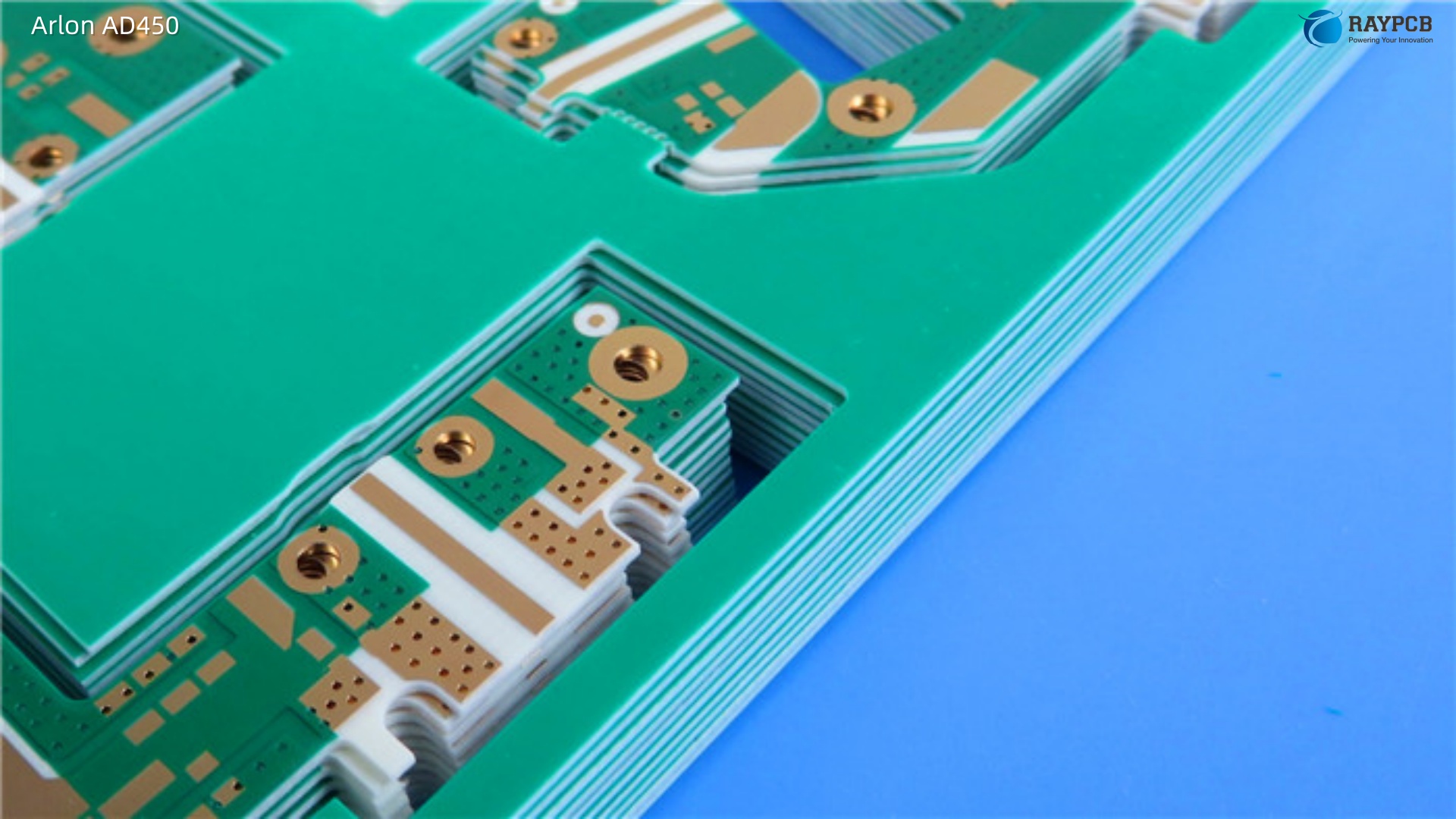
Arlon CLTE laminate is a ceramic powder-filled, woven micro-fiberglass reinforced PTFE composite engineered specifically for microwave and RF printed circuit board applications. The acronym “CLTE” stands for Controlled Low Thermal Expansion — and that name tells you exactly what problem it was designed to solve.
CLTE is a ceramic powder-filled and woven micro fiberglass reinforced PTFE composite engineered to produce a stable, low water absorption laminate with a nominal Dielectric Constant of 2.98. Arlon’s proprietary formulation creates a reduced Z-direction thermal expansion nearer to the expansion rate of copper metal, improving plated-through hole reliability.
The physics behind this are straightforward. Copper expands at roughly 17 ppm/°C in the Z direction. Standard PTFE-based laminates without ceramic loading can run 150–250 ppm/°C in Z — orders of magnitude higher. Every time your board goes through a reflow oven or a thermal cycle in the field, that mismatch puts enormous stress on your vias. Eventually, something gives.
Arlon’s approach to solving this was to load the PTFE matrix with a proprietary ceramic powder filler. The ceramic constrains the natural thermal expansion of the PTFE, pulling the Z-axis CTE dramatically closer to copper. The woven micro-fiberglass reinforcement adds dimensional stability in X and Y. The result is a substrate that behaves far more predictably across temperature extremes than you’d get from an unreinforced PTFE material.
Why Low CTE Matters for High-Reliability PCB Design
Before diving deeper into CLTE’s specs, it’s worth spending a moment on why Z-axis CTE is the critical variable in high-reliability designs. Engineers new to RF laminates sometimes focus exclusively on Dk and Df — and those do matter — but CTE mismatch is often the failure mode that actually kills boards in the field.
When a PCB heats up, the laminate expands. If that expansion rate differs significantly from copper, the barrel of each plated-through hole (PTH) gets stretched. Over thousands of thermal cycles — think aerospace hardware operating across a −55°C to +125°C range — micro-cracks form in the copper barrel. Resistance climbs. Eventually you get an open. In a radar manifold or phased array feed network, that’s a catastrophic failure.
A filled PTFE product such as Arlon’s CLTE-XT does not have a Tg in the range of 50 to 260°C (PTFE does not exhibit a glass transition such as is seen in thermoset materials), but because of the low expansion filler, has a low and consistent Z-direction expansion in that range, by virtue of which it will have excellent plated-through hole reliability.
That’s the core value proposition: matched CTE in Z, excellent PTH reliability, stable electrical performance across the temperature range your system actually operates in.
Arlon CLTE Core Properties and Specifications
Here’s what the datasheet tells you, organized for quick reference:
Electrical Properties
| Property | Typical Value | Test Condition |
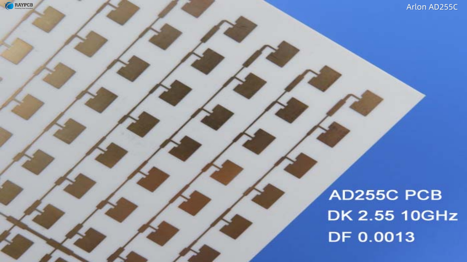
| Dielectric Constant (Dk) | 2.98 | 10 GHz |
| Dissipation Factor (Df) | 0.0016–0.0020 | 10 GHz |
| TCDk (Temperature Coefficient of Dk) | Very low | Across operating range |
| Dielectric Constant Stability | Thermally stable | Minimized 19°C phase transition effect |
Thermal and Mechanical Properties
| Property | Typical Value |
| Z-axis CTE | Matched nearer to copper (~17 ppm/°C range) |
| Thermal Conductivity | Higher than standard PTFE laminates |
| Water Absorption | Very low |
| Dimensional Stability | Excellent (woven glass reinforcement) |
One detail worth highlighting: the formulation was chosen to minimize the change in εr caused by the 19°C second-order phase transition in the molecular structure. This temperature-stable εr simplifies circuit design and optimizes circuit performance in applications such as phased array antennas.
That 19°C transition is a known headache with pure PTFE. Below that temperature, PTFE crystals rearrange, causing a step change in dielectric constant that throws off phase and impedance. The ceramic fill in CLTE suppresses this transition effect significantly — which is why CLTE is a much better choice than plain PTFE when your system needs to operate across the full −55 to +125°C range.
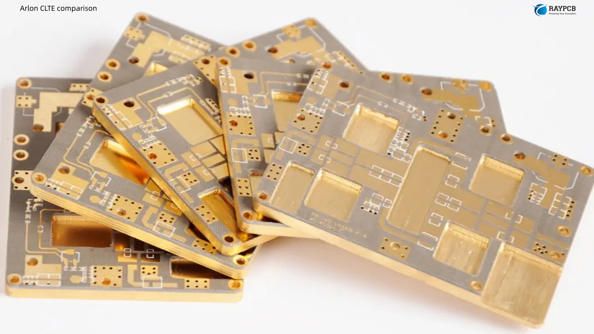
The CLTE Product Family: Choosing the Right Grade
Arlon has developed several variants around the core CLTE platform. Knowing the differences helps you specify the right grade without overpaying.
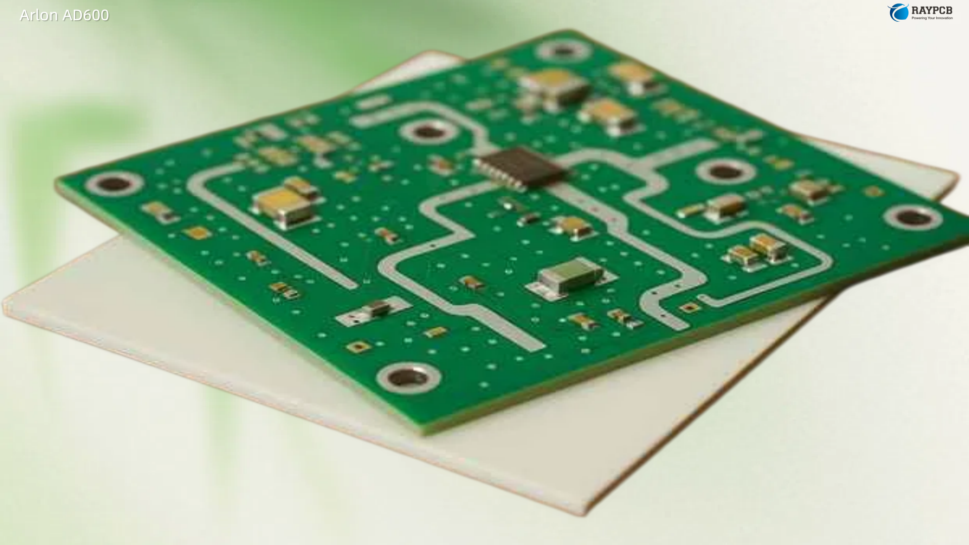
CLTE (Standard)
The base product. Ceramic/PTFE composite with woven micro-fiberglass reinforcement, Dk of 2.98, good thermal conductivity, low Df, stable Dk vs temperature. The right choice for most defense and satellite microwave applications where you need proven, reliable performance without the tightest possible tolerances.
CLTE-XT (Extended — Premium Grade)
CLTE-XT has “Best-in-Class” Insertion Loss (S21) and Loss Tangent (0.0012). During development, Arlon focused not only on reducing Loss Tangent, but also on reducing Conductive Losses. As a result, CLTE-XT Insertion Loss is “Best-In-Class”.
CLTE-XT tightens Dk tolerance to ±0.03 and delivers the lowest insertion loss in its class. CLTE-XT has the lowest loss, lowest thermal expansion, highest phase stability, and lowest moisture absorption of any product in its class. Use this when you’re building phase-sensitive filter applications, SIGINT electronics, or anything where you need maximum phase stability and the narrowest possible Dk tolerance.
CLTE-AT (Affordable Tier)
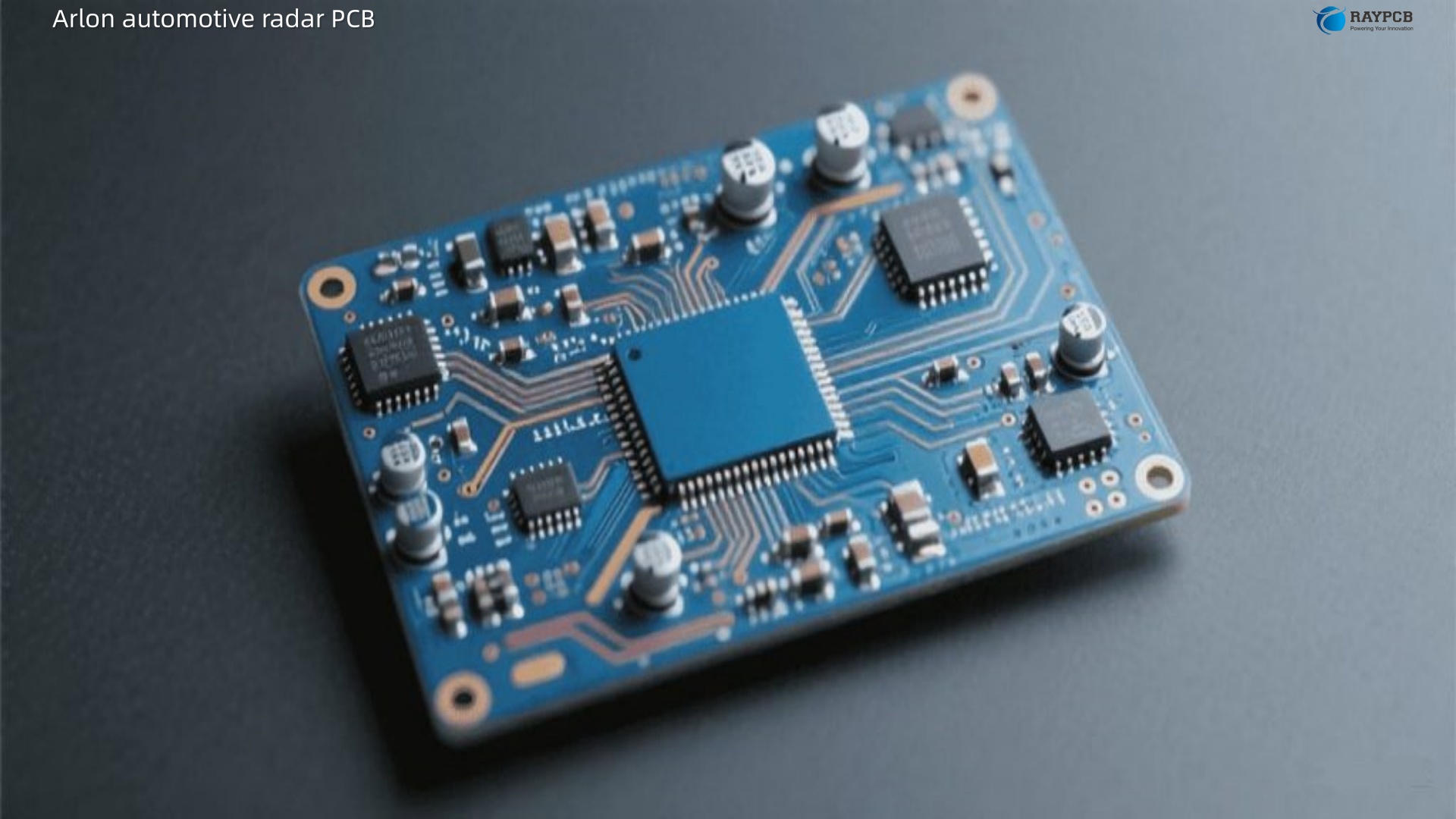
CLTE-AT laminates use the common building blocks developed with CLTE-XT laminates, but with some changes to make the product more affordable. This results in a higher dielectric constant (3.00) and a slightly different thickness than the CLTE-XT laminates. CLTE-AT is a solid choice for automotive radar and adaptive cruise control applications — high-volume, cost-sensitive, but still requiring good CTE performance and phase stability.
CLTE-LC (Low Cost)
Arlon’s CLTE-LC is a ceramic-filled, woven fiberglass reinforced PTFE composite engineered to produce a dimensionally and electrically stable, low water absorption laminate with a nominal dielectric constant of 2.94. It is designed to offer all of the same properties and functionality as Arlon’s CLTE, but in most cases at a reduced cost. If your application fits CLTE but budget is a constraint, CLTE-LC is worth evaluating.
Quick Comparison Table
| Grade | Dk (10 GHz) | Df | Dk Tolerance | Best For |
| CLTE | 2.98 | ~0.0016–0.0020 | ±0.05 | Radar, satellite, defense microwave |
| CLTE-XT | 2.94 | 0.0012 | ±0.03 | Phase-sensitive, SIGINT, space |
| CLTE-AT | 3.00 | 0.0013 | ±0.04 | Automotive radar, commercial RF |
| CLTE-LC | 2.94 | ~0.0016–0.0020 | ±0.05 | Cost-sensitive defense/commercial |
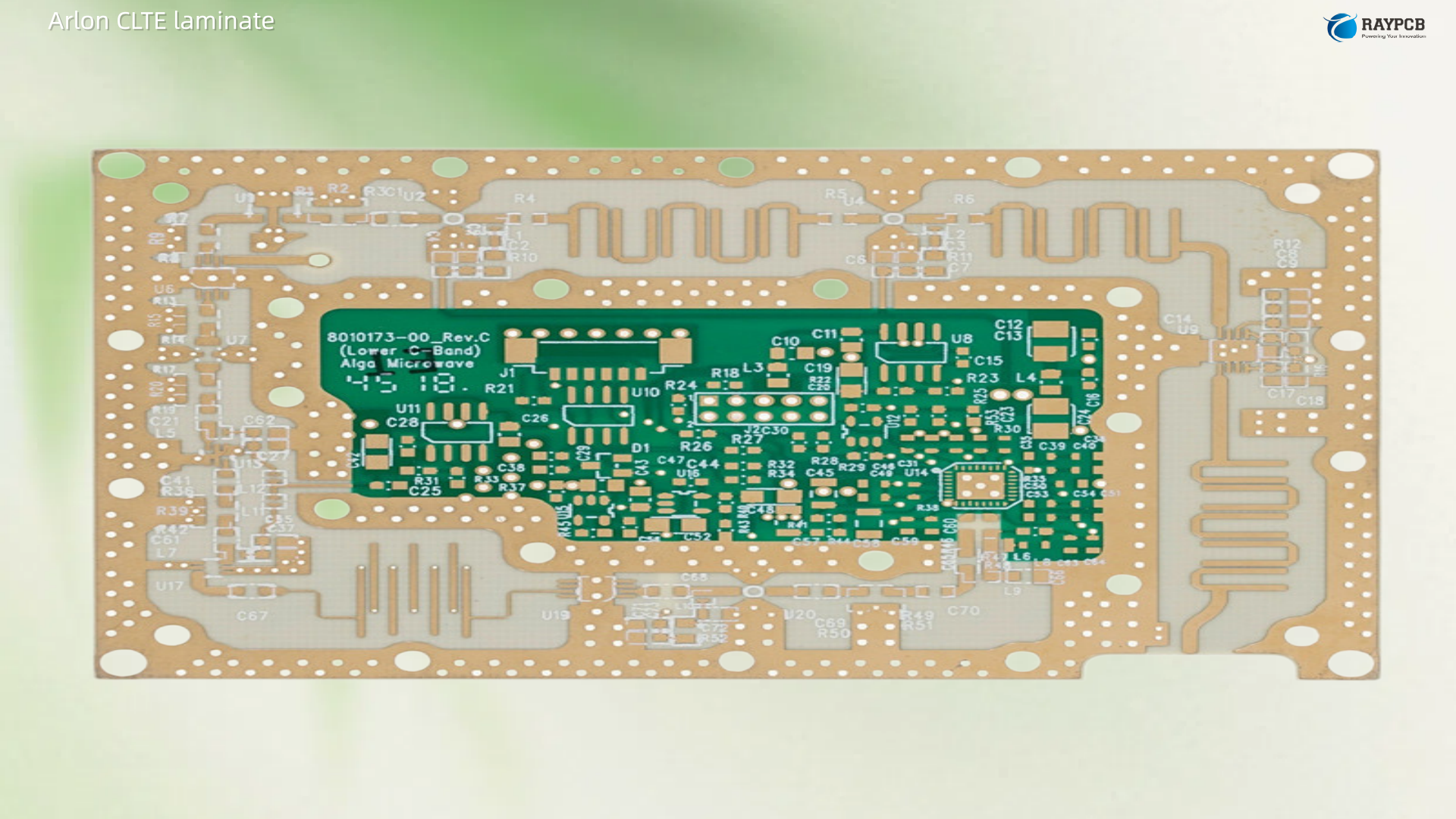
Key Applications for Arlon CLTE Laminate
Typical applications include radar manifolds, phased array antennas, microwave feed networks, phase-sensitive electrical structures, PAs, LNAs, LNBs, and satellite and space electronics.
Let me break down why CLTE is specifically well-suited for each of these:
Phased Array Antennas
This is probably the most common application you’ll encounter. Phased arrays rely on precise phase control across many radiating elements. Any Dk variation with temperature translates directly to phase error. The temperature-stable εr simplifies circuit design and optimizes circuit performance in applications such as phased array antennas. With CLTE, your Dk stays consistent whether the array is sitting on a cold ramp in Alaska or running hot in the Middle East.
Radar Manifolds
Radar front ends — especially AESA (Active Electronically Scanned Array) radar — use complex power distribution manifolds where every millimeter of trace length contributes to phase and amplitude balance. Dimensional stability of the substrate matters enormously. CLTE’s low X-Y CTE and woven glass reinforcement keep feature dimensions tight across the manufacturing process and across temperature.
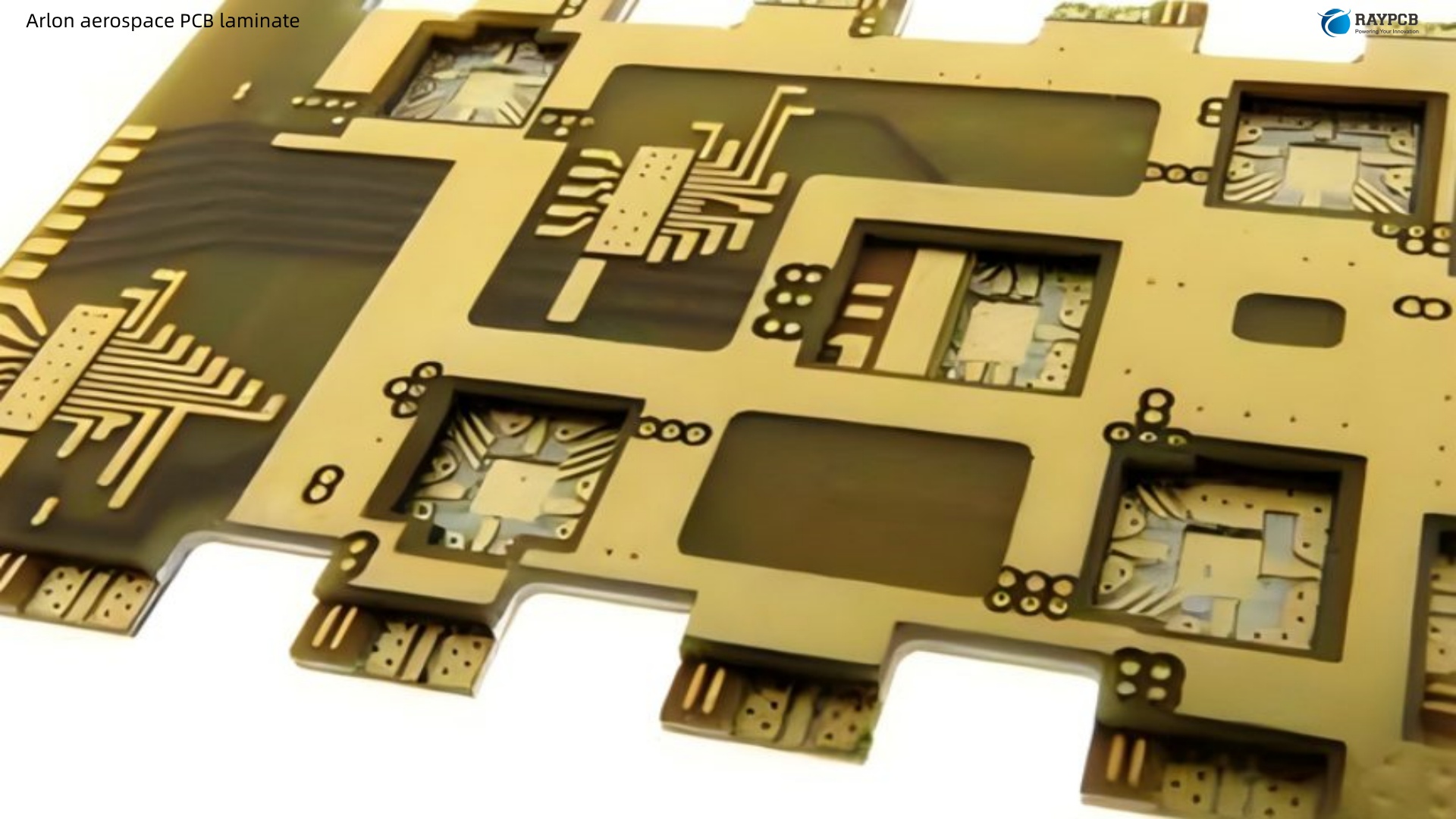
Satellite and Space Electronics
CLTE can be made into 64 layers at most on global communication satellites. The combination of low water absorption, stable Dk vs temperature, excellent PTH reliability, and high thermal conductivity makes CLTE a natural fit for space-qualified electronics. In the vacuum of orbit, outgassing and moisture retention are real concerns — CLTE’s low moisture absorption addresses these directly.
Microwave Feed Networks
Combiner/divider networks, beam-forming networks, and corporate feed structures for antenna arrays benefit from CLTE’s consistent impedance across temperature. When you’re splitting power across 64 or 128 channels, any impedance mismatch ripples through the whole system as amplitude and phase imbalance.
Power Amplifiers and LNAs
CLTE also provides higher thermal conductivity that increases the rate of heat dissipation and thus permits use of higher power in an otherwise equivalent design. In PA boards especially, heat management is inseparable from electrical performance. CLTE’s improved thermal conductivity gives designers margin they wouldn’t have with standard PTFE.
Fabrication Considerations for CLTE PCBs
CLTE is a PTFE-based material, which means your standard FR-4 shop processes won’t apply without modification. Here are the key fabrication considerations any PCB engineer should know:
Drilling
Ceramic-filled PTFE is harder on drill bits than FR-4. Expect more frequent bit changes, and ensure your board house uses sharp bits and appropriate feed/speed parameters. The ceramic particles accelerate bit wear — a fabricator who doesn’t adjust will give you sloppy holes and poor barrel quality.
Multilayer Lamination
CLTE prepreg (designated CLTE-P) requires elevated lamination temperatures. CLTE-P requires a lamination temperature of 550°F/572°F (288–300°C) to allow sufficient flow of the resin. The lamination temperature should be measured at the bond line using a thermocouple located in the edge of the product panel. This is significantly higher than standard epoxy prepreg lamination, and not all press equipment can handle it. Verify your fabricator’s capabilities before designing multilayer CLTE stacks.
Surface Treatment
Unlike FR-4, PTFE-based materials are inherently non-stick. Proper surface activation before copper plating is essential. Most shops use sodium etching or plasma treatment on PTFE surfaces to achieve adequate bond strength. Skipping this step is a recipe for delamination.
Panelization and Routing
PTFE composites machine differently from rigid thermosets. Use carbide tooling, slower feed rates, and consistent coolant/air blast to get clean edges without smearing.
Arlon CLTE vs. Competing Materials
Engineers evaluating CLTE often compare it against Rogers’ RO3003 or RO4003 series. Here’s a practical comparison:
| Parameter | Arlon CLTE | Rogers RO3003 | Rogers RO4003C |
| Dk (10 GHz) | 2.98 | 3.00 | 3.55 |
| Df (10 GHz) | ~0.0016–0.0020 | 0.0010 | 0.0027 |
| Z-CTE | Very low (near copper) | Low | Moderate |
| Water Absorption | Very low | Very low | Low |
| Multilayer capability | Excellent | Good | Good |
| Max layer count (reported) | Up to 64 | Typically fewer | Typically fewer |
| Relative Cost | Premium | Premium | Moderate |
The comparison isn’t always about which material is “better” overall — it’s about which material fits your specific combination of frequency, thermal environment, layer count, and budget. For deep defense applications requiring maximum phase stability and high layer count, CLTE’s proprietary formulation gives it a strong argument. For single/dual layer commercial microwave boards, RO4003C may offer a simpler fabrication path at lower cost.
For a comprehensive overview of Arlon PCB material families beyond CLTE — including polyimide, epoxy, and other PTFE-based products — it’s worth reviewing the full Arlon portfolio to find the right match for your application.
Design Tips for Getting the Most Out of CLTE
A few things from real-world design experience that don’t always make it into datasheets:
Match your stack-up carefully. CLTE prepreg (CLTE-P) is matched in Dk to CLTE laminates. Don’t mix in standard FR-4 prepreg in a CLTE multilayer stack — the Dk discontinuity will wreck your controlled impedance layers.
Account for Dk variation with thickness. Especially on thin substrates (0.005″ and 0.010″), Dk varies with nominal thickness. The CLTE-XT datasheet explicitly lists design Dk values per thickness. Always design from that table rather than assuming the bulk Dk applies uniformly.
Specify copper foil treatment. Rougher copper foils give better peel strength but increase conductor loss at high frequencies — the skin effect causes current to flow in the rough surface features, increasing resistance. Arlon has designed CLTE-XT specifically to achieve good peel strength with smoother copper, preserving insertion loss performance. Specify low-profile copper if your application is loss-sensitive above 10 GHz.
Thermal via strategy. CLTE’s improved thermal conductivity helps, but for PA boards with significant power dissipation, pair it with a thermal via array under your active devices. The improved laminate conductivity complements, rather than replaces, proper thermal management design.
Useful Resources for PCB Engineers Working with CLTE
| Resource | What You’ll Find | URL |
| Arlon CLTE Datasheet | Full electrical, thermal, mechanical specs | arlonemd.com |
| Arlon Microwave & RF Materials Guide | Comparison across the full PTFE/ceramic product line | Available via Arlon sales |
| IPC-4103 Slash Sheet | Specification standard for PTFE/ceramic laminates | ipc.org |
| Arlon Laminate Design Guide | Practical guidance on high-performance laminate selection | arlonemd.com |
| UL Prospector — Arlon | Material database with property searches | ulprospector.com |
| Cirexx Arlon Materials Overview | Fabricator’s perspective on CLTE in production | cirexx.com/arlon-materials |
Always pull the latest version of the datasheet directly from Arlon or your authorized distributor — properties are revised periodically as formulations are refined.
Real-World Reliability: What CLTE Delivers Over Time
The question engineers actually care about isn’t just what CLTE looks like on a datasheet — it’s whether it holds up over thousands of thermal cycles in the field. The answer, based on decades of deployment in defense and satellite systems, is that it does — when fabricated correctly.
CLTE is stable during subsequent thermal cycling in process, assembly and use. The key phrase there is “when fabricated correctly.” Arlon’s ceramic/PTFE composite relies on proper surface activation, correct lamination temperatures, and appropriate via-filling practices to deliver that long-term reliability. A poorly executed CLTE build will fail just as surely as a cheaply specified one.
For programs requiring long-life electronics — 20-year satellite missions, airborne radar systems with hard MTBF targets — the combination of low Z-CTE and thermally stable Dk makes CLTE a defensible material choice that holds up under design review scrutiny. When your program office asks why you chose a premium laminate, “matched CTE to copper and stable Dk across −55 to +125°C” is an answer that holds up.
Frequently Asked Questions About Arlon CLTE Laminate
Q1: What does the “CLTE” acronym actually stand for?
CLTE stands for Controlled Low Thermal Expansion. The name directly reflects the material’s primary design intent: using ceramic filler in a PTFE matrix to reduce the coefficient of thermal expansion, particularly in the Z direction, bringing it much closer to the expansion rate of copper conductors. This dramatically improves plated-through hole reliability over thermal cycling.
Q2: Can I use standard FR-4 fabrication processes for CLTE boards?
No — not without significant process modifications. PTFE-based materials like CLTE require different surface preparation (plasma or sodium etch for via hole treatment), higher lamination temperatures for prepreg processing (288–300°C vs. ~180°C for standard epoxy prepreg), and more careful drill bit management due to ceramic filler wear. Work with a fabricator who has documented experience with PTFE laminates, not just FR-4.
Q3: What is the difference between CLTE and CLTE-XT?
CLTE-XT is a premium refinement of the base CLTE platform. It offers the lowest loss tangent (0.0012) and tightest Dk tolerance (±0.03) in the family, along with the lowest thermal expansion and highest phase stability. CLTE-XT is optimized for phase-sensitive and SIGINT applications where every fraction of a dB and every degree of phase matters. Standard CLTE is still the right choice for most defense and satellite microwave applications — CLTE-XT is for the most demanding phase-critical systems.
Q4: Is Arlon CLTE suitable for lead-free (RoHS-compliant) assembly?
Yes. CLTE’s low CTE and thermal stability make it suitable for lead-free solder assembly processes, which operate at higher temperatures than tin-lead soldering. The ceramic/PTFE composite maintains its properties through reflow without the delamination risk that higher-CTE materials carry. That said, always verify your specific assembly parameters with Arlon’s fabrication guidelines, particularly for thick multilayer stackups.
Q5: How does CLTE compare to Rogers RO3003 for phased array antenna applications?
Both are ceramic/PTFE composites with very similar Dk values (~3.0) and both are used extensively in phased array hardware. The main differences are in Df (RO3003 is typically slightly lower at 0.0010 vs. CLTE’s ~0.0016–0.0020), multilayer capability (CLTE has a well-documented track record in very high layer count builds, including up to 64 layers in satellite applications), and sourcing/supply chain considerations. For programs requiring U.S.-origin materials and high layer count multilayers, CLTE has strong advantages. For lower layer count boards where insertion loss is the primary driver, RO3003 is a competitive alternative.
Meta Description Suggestion:
Arlon CLTE laminate is a ceramic/PTFE composite substrate engineered for low thermal expansion and stable Dk in high-reliability PCBs. Learn key specs, CLTE vs CLTE-XT comparison, fabrication tips, and applications in radar, phased arrays, and satellite electronics — written for working PCB engineers.