Arlon DiClad 880 is a woven PTFE/fiberglass laminate with Dk 2.17–2.20 and Df 0.0009 at 10 GHz — the lowest loss in the DiClad series. Complete engineer’s guide covering DiClad 880 specs, datasheet, thickness options, fabrication guidelines, and applications in military radar, missile guidance, and phased array PCBs.
There’s a certain category of microwave circuit where every fraction of a dB matters and where signal propagation speed is not just a datasheet talking point but a genuine system-level constraint. Missile guidance, military radar feed networks, low noise amplifier front ends, high-speed digital radio antennas — these are the applications where material selection is not a procurement afterthought but a core engineering decision. Arlon DiClad 880 was built for exactly that category.
With a dielectric constant of 2.17 or 2.20 and a dissipation factor of 0.0009 at 10 GHz, DiClad 880 delivers the lowest Dk and lowest loss available in the woven fiberglass-reinforced PTFE laminate family. If you’re designing circuits that need the fastest signal propagation and the smallest insertion loss penalty from the substrate, DiClad 880 is where you start.
This guide covers the complete picture: material construction, key specifications, available configurations, application breakdown, fabrication requirements, comparison with competing laminates, and the practical engineering judgment calls you need to make when DiClad 880 is on the table.
What Is Arlon DiClad 880?
Arlon DiClad 880 is a woven fiberglass/PTFE composite laminate that uses a low fiberglass/PTFE ratio to deliver the lowest dielectric constant and dissipation factor in the DiClad series. The “880” designation places it at the high-performance, low-Dk end of Arlon’s DiClad product family, which spans dielectric constants from 2.17 up to 2.65 depending on fiberglass loading.
The material achieves its ultra-low Dk through a deliberate compositional strategy: by minimizing the amount of woven fiberglass reinforcement and maximizing the PTFE fraction of the composite, Arlon pushes the effective dielectric constant of the composite down toward the intrinsic Dk of PTFE itself (approximately 2.1). The tradeoff is mechanical — lower fiberglass content means less rigidity and dimensional stability compared to more heavily reinforced PTFE laminates. DiClad 880 is explicitly engineered to prioritize electrical performance over mechanical convenience, which is exactly the right tradeoff for its target applications.
The coated fiberglass plies in DiClad materials are aligned in the same direction — this is the unidirectional construction that distinguishes DiClad from the cross-plied CuClad family. For applications where the primary requirement is the lowest possible Dk and loss rather than in-plane electrical isotropy, that unidirectional construction delivers the electrical performance targets at lower cost.
DiClad 880 Key Electrical Properties and Datasheet Specifications
Core Electrical Properties
| Property | Value | Test Condition |
| Dielectric Constant (Dk) | 2.17 or 2.20 | 10 GHz |
| Dissipation Factor (Df) | 0.0009 | 10 GHz |
| Dk Stability vs. Frequency | Highly uniform across frequency | RF to microwave |
| Electrical Property Uniformity | Excellent across panel | Consistency of PTFE coating process |
The Df of 0.0009 at 10 GHz is not just a low number in an abstract sense — it represents one of the lowest dissipation factors achievable in a woven fiberglass-reinforced laminate. For reference, laminates based on PTFE and reinforced with woven glass can be manufactured with low Dk (2.17) and loss as low as 0.0009 at 10 GHz. Standard FR-4 runs Df values of 0.020 or higher at high frequency — DiClad 880’s Df is more than 20 times lower.
Physical and Mechanical Properties
| Property | Description |
| Reinforcement | Unidirectional woven fiberglass |
| Matrix | PTFE (polytetrafluoroethylene) |
| Fiberglass/PTFE ratio | Low (maximizes PTFE fraction) |
| Dimensional stability | Excellent vs. non-woven PTFE laminates |
| Dk uniformity | Better than non-woven PTFE laminates |
| Water absorption | Very low (PTFE-based) |
| Chemical resistance | Excellent |
| Copper cladding | Standard and heavy weights available |
Available Thicknesses and Dk Options
From the Arlon Microwave & RF Materials Guide, DiClad 880 is available in the following configurations:
| Thickness (inches) | Thickness (mm) | Available Dk Options |
| 0.005″ | 0.127 | 2.17, 2.20 |
| 0.010″ | 0.254 | 2.17, 2.20 |
| 0.015″ | 0.381 | 2.17, 2.20 |
| 0.020″ | 0.508 | 2.17, 2.20 |
| 0.030″ | 0.762 | 2.17, 2.20 |
| 0.050″ | 1.270 | 2.17, 2.20 |
| 0.060″ | 1.524 | 2.17, 2.20 |
| 0.125″ | 3.175 | 2.17, 2.20 |
| 0.040″ | 1.016 | 2.40, 2.45, 2.50, 2.55, 2.60 |
Master sheet sizes include 36″ × 72″, 36″ × 48″, and 36″ × 36″. The 36″ × 72″ option is notably larger than most competing PTFE laminates offer as a standard format — relevant for phased array aperture boards and large combiner panels where maximizing usable area from a single sheet reduces fabrication waste and cost.
Note the 0.040″ thickness row where higher Dk options (2.40–2.60) are listed — this represents availability of the higher-glass-ratio DiClad 527 series at that specific thickness in the same product family ordering system.
Understanding DiClad 880’s Construction: Why Unidirectional Ply Matters
The fiberglass ply orientation is one of those details that engineers sometimes gloss over when pulling specs from a material comparison table. For DiClad 880, it’s worth understanding the implications.
The coated fiberglass plies in DiClad materials are aligned in the same direction. This unidirectional construction is distinct from the cross-plied architecture used in Arlon’s CuClad family. The consequence is that DiClad 880 has a small degree of electrical anisotropy — the Dk is marginally different depending on whether you’re measuring along the fiber direction or perpendicular to it. The magnitude of this anisotropy in practice is small, but in circuits where uniformity in all directions matters, it’s worth knowing.
What unidirectional construction gives you in return is superior Dk uniformity within-plane, along the fiber direction, and the absolute lowest loss achievable at a given Dk target. It also allows for larger sheet formats and somewhat simpler manufacturing process control compared to the precision alignment required for cross-plied construction.
The woven fiberglass reinforcement in DiClad products provides greater dimensional stability than nonwoven fiberglass-reinforced PTFE laminates of similar dielectric constants. The consistency and control of the PTFE-coated fiberglass cloth allows Arlon to produce a laminate with better Dk uniformity than comparable non-woven fiberglass-reinforced laminates. This matters on large panels — a Dk gradient across a 36″ × 48″ panel translates directly to performance variation across a large aperture antenna or a multi-channel power divider network.
DiClad 880 Performance Features: What the Numbers Mean in Practice
Extremely Low Loss Tangent — What 0.0009 Actually Buys You
The Df = 0.0009 at 10 GHz headline is worth translating into practical circuit terms. Dielectric loss contributes to total insertion loss in a transmission line alongside conductor loss. At microwave frequencies on a typical 50Ω microstrip, the dielectric loss per unit length is directly proportional to Df. Cutting Df from 0.020 (FR-4 level) to 0.0009 (DiClad 880) reduces the dielectric contribution to insertion loss by a factor of more than 20.
In a 10 GHz LNA front end, that difference between substrate losses is the difference between a commercially acceptable noise figure and a board that’s burning your system noise budget before the signal even reaches the first active device. In a long radar feed manifold distributing power across 64 elements, the cumulative insertion loss from substrate Df adds up at every branch and every inch of transmission line. DiClad 880’s 0.0009 Df is the right answer when you need to minimize that cumulative loss budget.
Electrical Properties Highly Uniform Across Frequency
One of DiClad 880’s explicitly listed benefits is that electrical properties are highly uniform across frequency. For wideband designs — swept-frequency filter characterization, multi-octave amplifiers, digital radio systems with wide instantaneous bandwidth — this stability simplifies design. If your substrate Dk drifts with frequency, your impedance calculations at the design center frequency don’t hold at the band edges. DiClad 880’s PTFE-based composition inherently produces a very flat Dk vs. frequency curve, which means the same design parameters work across your full frequency range.
Consistent Mechanical Performance and Chemical Resistance
Excellent chemical resistance and consistent mechanical performance are two properties that matter in harsh-environment electronics. PTFE is inherently resistant to most chemicals and solvents used in PCB fabrication and assembly — acid etches, flux residues, cleaning solvents. The material won’t absorb process chemicals that could alter its dielectric properties over time. In avionics, missile systems, and ground-based radar that may be exposed to fuel, hydraulic fluid, or cleaning agents, that chemical inertness is a real reliability advantage.
Arlon DiClad 880 Typical Applications
Military Radar Feed Networks
This is the application DiClad 880 was designed around. Radar feed networks — particularly the complex power distribution manifolds feeding phased array apertures — are among the highest-performance microwave circuits built on organic substrates. The combination of ultra-low loss (to maximize radiated power) and low Dk (to enable compact, high-impedance line widths on thin substrates) makes DiClad 880 the natural choice for this class of circuit.
Missile Guidance Systems
Missile guidance RF circuits face a compound specification challenge: they need to function across extreme temperature ranges (from cold storage through aerodynamic heating), survive high-g shock and vibration loads, and deliver precise electrical performance in a compact, lightweight package. DiClad 880’s chemical resistance, stable electrical properties, and consistent mechanical performance address all three axes of this challenge. Low water absorption means no dielectric property shift from humidity cycling during storage.
Commercial Phased Array Networks
Commercial phased array systems — including base station antenna arrays for cellular infrastructure and satellite ground terminals — need low-loss substrates at a price point compatible with commercial volume production. DiClad 880 occupies a favorable position here: it delivers near-maximum PTFE performance with the improved dimensional consistency of woven (rather than non-woven) fiberglass reinforcement, enabling tighter production tolerances on electrical performance without the cost premium of ceramic-filled PTFE systems.
Low Loss Base Station Antennas and Digital Radio Antennas
For base station antenna boards where insertion loss in the feed network translates directly to effective radiated power (and therefore to coverage or required PA power), substrate Df is a first-order design variable. DiClad 880 at Df = 0.0009 enables low-loss combiner networks that maximize the power actually reaching the radiating elements rather than dissipating it in the laminate.
Filters, Couplers, and Low Noise Amplifiers
DiClad laminates are frequently used in filter, coupler, and low noise amplifier applications where dielectric constant uniformity is critical. In bandpass filters, Dk uniformity across the panel is the primary determinant of center frequency repeatability from board to board. In couplers and LNAs, low loss is the critical variable. DiClad 880’s combination of high PTFE content (for low Df) and woven fiberglass reinforcement (for Dk uniformity) positions it as a natural choice for all three circuit types.
For a comprehensive overview of the full Arlon PCB material catalog — covering the entire range from woven PTFE laminates through ceramic-filled PTFE composites, polyimide systems, and high-speed epoxies — it’s valuable to understand DiClad 880 in the context of the complete Arlon portfolio.
Arlon DiClad 880 Within the DiClad Family
Understanding where DiClad 880 sits in the DiClad series helps you make confident material selection decisions:
| DiClad Grade | Dk Range | Df (10 GHz) | Fiberglass/PTFE Ratio | Best For |
| DiClad 880 | 2.17 – 2.20 | 0.0009 | Lowest | Ultra-low loss, fastest propagation |
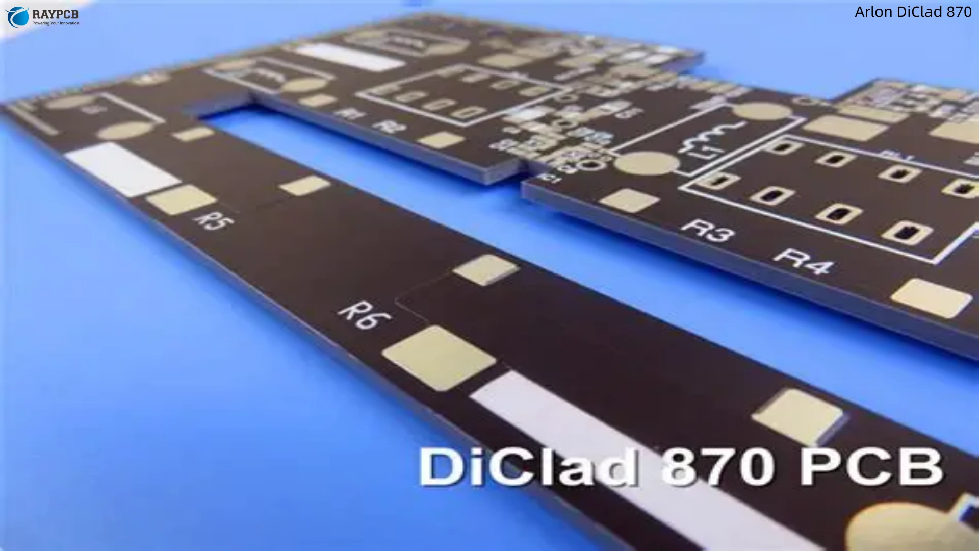
| DiClad 870 | ~2.33 | ~0.0013 | Medium | Balanced loss / mechanical properties |
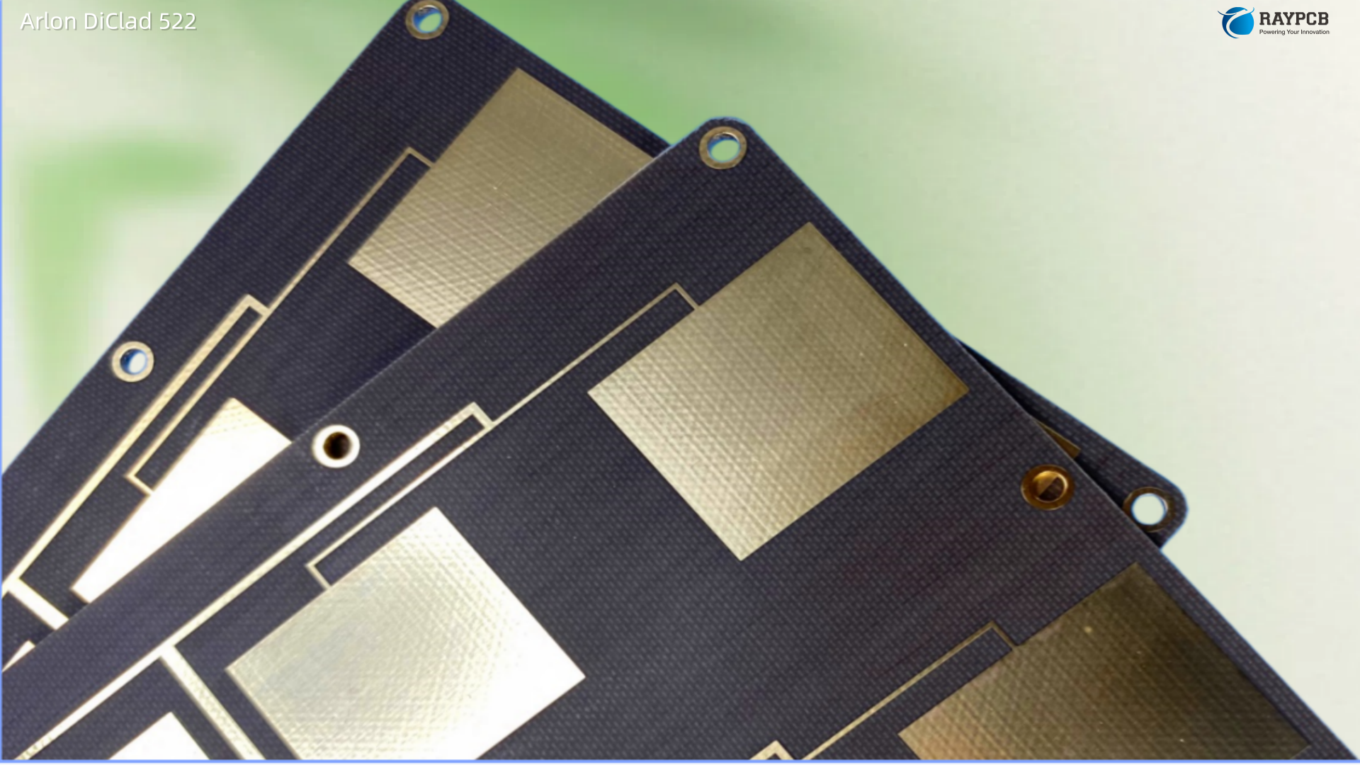
| DiClad 522 | 2.40 – 2.65 | ~0.0015–0.0022 | Higher | Better dimensional stability, conventional-like mechanicals |
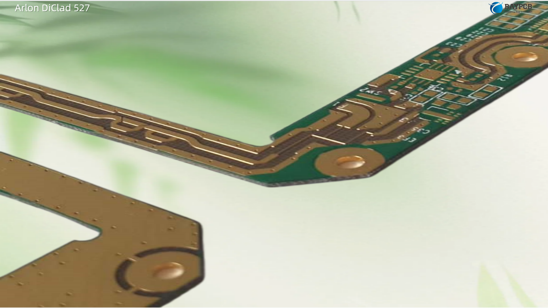
| DiClad 527 | 2.40 – 2.65 | ~0.0015–0.0022 | Higher | Better dimensional stability, lower thermal expansion |
DiClad 880 and the DiClad 870 sit at the electrical performance end of the DiClad range — they sacrifice some mechanical robustness for the lowest achievable Dk and loss. DiClad 522 and 527 move in the other direction, using more fiberglass to gain mechanical stability and lower CTE, closer to conventional substrates in behavior if not quite there.
The practical selection rule: if lowest loss and Dk are the primary requirements, specify DiClad 880. If you need better mechanical stability and can tolerate slightly higher Dk and Df, DiClad 870 or the 522/527 family are the right steps up the mechanical stiffness ladder.
DiClad 880 vs. Competing Low-Dk Laminates
Engineers specifying DiClad 880 typically also evaluate Rogers RT/duroid 5880 and Taconic TLY-5. Here’s an honest comparison:
| Parameter | Arlon DiClad 880 | Rogers RT/duroid 5880 | Taconic TLY-5 |
| Dk (10 GHz) | 2.17 / 2.20 | 2.20 | 2.17 |
| Df (10 GHz) | 0.0009 | 0.0009 | 0.0009 |
| Construction | Unidirectional woven glass/PTFE | PTFE/microfiber glass | PTFE/woven glass |
| Dimensional stability | Good (woven reinforcement) | Moderate | Good |
| Dk uniformity | Excellent (woven control) | Good | Good |
| Max sheet size | 36″ × 72″ | 30″ × 24″ std | Varies |
| Panel-level Dk consistency | Excellent | Good | Good |
At the electrical property level, these three materials are essentially equivalent — all hitting Dk ≈ 2.17–2.20 and Df = 0.0009 at 10 GHz. The differentiation comes in manufacturing process, Dk uniformity control, sheet size availability, and supply chain considerations. DiClad 880’s woven fiberglass construction gives it a dimensional stability and Dk uniformity advantage over RT/duroid 5880’s microfiber glass construction. The larger available sheet sizes (36″ × 72″ for DiClad 880 vs. 30″ × 24″ standard for RT/duroid 5880) matter for large-format aperture boards.
Fabrication Guidelines for Arlon DiClad 880 PCBs
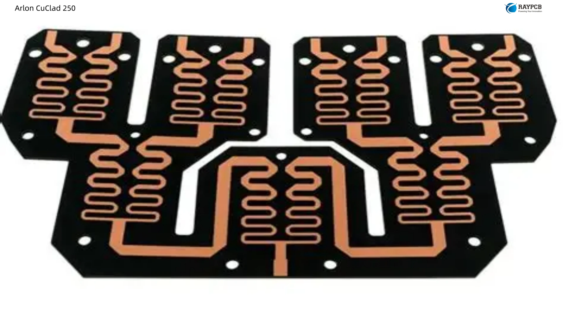
DiClad 880 is a PTFE-based material and requires PTFE-aware process controls throughout fabrication. The lower fiberglass content compared to DiClad 522/527 or CuClad 250 makes it somewhat softer and more susceptible to mechanical damage than higher-glass laminates, so process care is more important.
Drilling
Use highly polished carbide drill bits. Repointed (resharpened) drill bits are not recommended — even minor dulling on PTFE materials leads to tearing and smearing around the hole wall. DiClad 880’s low fiberglass content makes the laminate softer and more prone to drill-induced deformation than higher-glass PTFE products. Use appropriate entry and backup materials. Panels can be drilled in stacks, but keep total stack thickness within the limits your drill parameters are qualified for.
Surface Activation Before Plating and Bonding
PTFE is non-wetting by nature. Without surface activation, electroless copper will not adhere reliably to hole walls. Use inert gas plasma or sodium etch processes to activate PTFE surfaces before through-hole plating. Proceed to plating as quickly as practical after surface activation — the activated surface reverts toward its native non-wetting state over time (within a few hours). Adhesion to copper surfaces can be improved with an aggressive micro-etch such as ammonium persulfate prior to bonding in multilayer stacks.
Multilayer Bonding
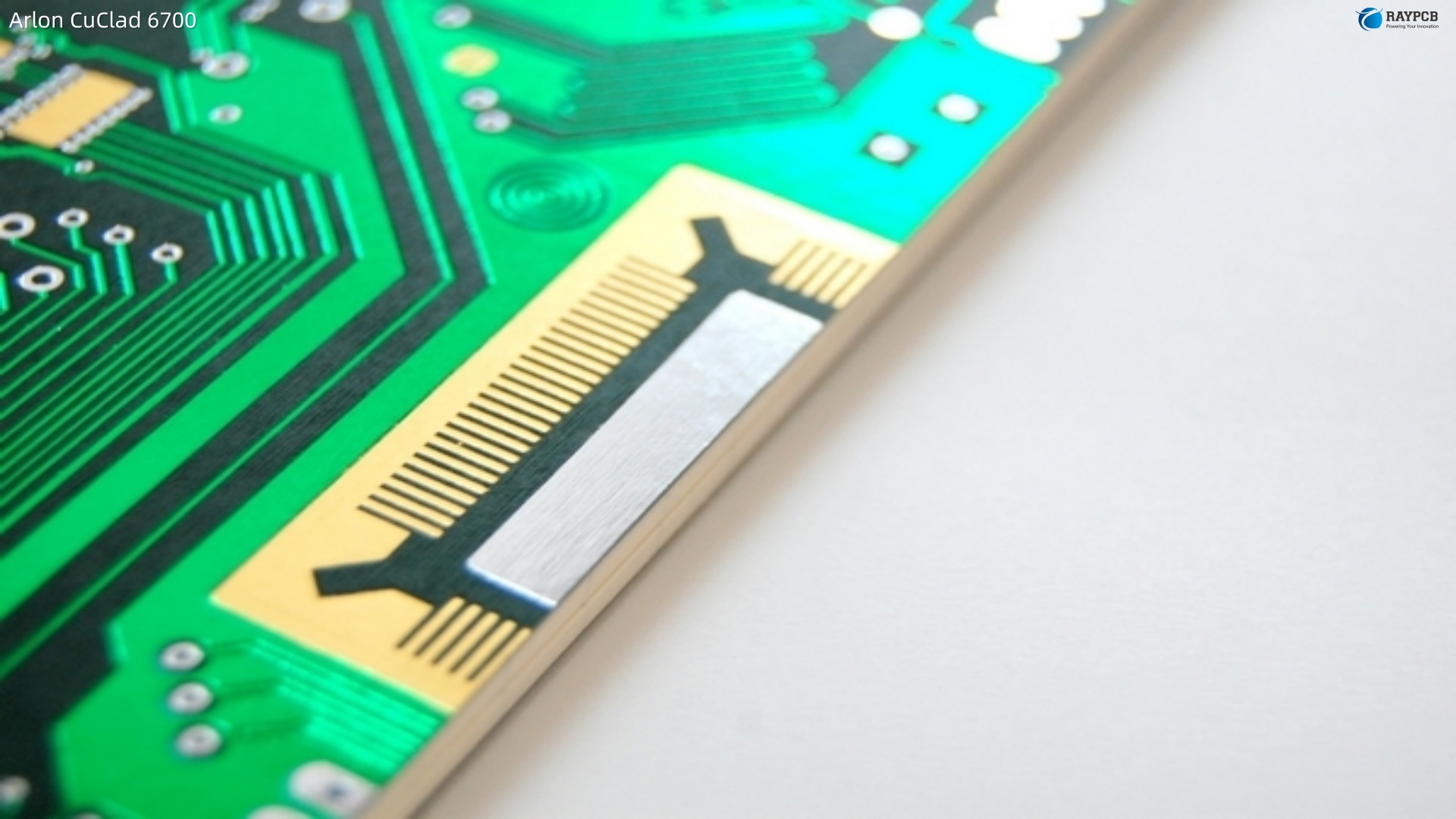
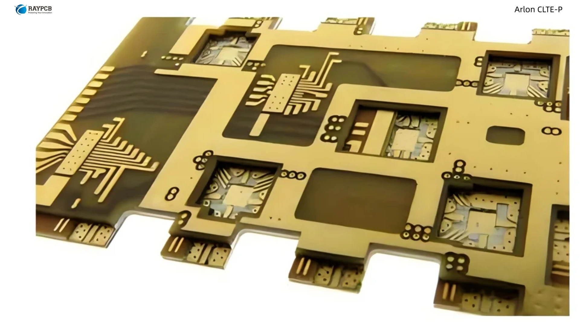
PTFE multilayer stacks using DiClad 880 core laminates require compatible bonding materials. Options include Arlon’s thermoplastic bonding films (CuClad 6700, CuClad 6250) or the CLTE-P bonding ply for Dk-matched bonding layers. Standard epoxy prepreg is not a good choice for controlled-impedance microstrip or stripline designs through DiClad 880 core material — the Dk mismatch at the bondline will throw off your impedance calculations.
Routing and Edge Preparation
Use two-flute, slow-spiral, micrograin carbide upcut endmills for routing. The low fiberglass content of DiClad 880 makes it more susceptible to edge tearing than higher-glass PTFE laminates, so proper feed rate control and sharp tooling are especially important. Support the panel with rigid entry and backup materials.
Storage and Handling
Store flat in a cool, dry location away from direct sunlight. Avoid bending or flexing the material — the low fiberglass content makes DiClad 880 less rigid than conventional substrates, and repeated handling stress can cause micro-cracking in the PTFE matrix over time. Keep panels in their original packaging until ready for processing.
Useful Resources for Engineers Specifying DiClad 880
| Resource | What You’ll Find | Where to Access |
| Arlon DiClad Datasheet (RS Online PDF) | Full DiClad family specs including DiClad 880 properties | docs.rs-online.com/9321/0900766b802b272f.pdf |
| Rogers DiClad 870/880 Product Page | Rogers-era product info and Laminate Properties Tool | rogerscorp.com/advanced-electronics-solutions/diclad-series-laminates/diclad-870_880-laminates |
| Arlon Microwave & RF Materials Guide | Full thickness/Dk availability tables, product family overview | integratedtest.com/wp-content/uploads/2021/08/ArlonMaterials.pdf |
| Fabrication Guidelines: DiClad, CuClad, IsoClad | PTFE process guidelines for drilling, bonding, routing | rfglobalnet.com/doc/fabrication-guidelines-arlon-diclad-cuclad-is-0001 |
| MatWeb — Arlon DiClad 880 | Material database entry for DiClad 880 properties | matweb.com |
| LookPolymers — DiClad 880 | Condensed DiClad 880 property summary | lookpolymers.com |
| IPC-4103 | Industry specification standard for PTFE-based laminates | ipc.org |
| Arlon EMD Laminate Design Guide | Comprehensive high-performance laminate selection guidance | arlonemd.com/wp-content/uploads/2020/05/Laminate-Guide.pdf |
Always verify specifications from the current Rogers Corporation datasheet — Rogers acquired Arlon Circuit Materials in 2015, and the authoritative current spec documents are maintained under the Rogers brand.
Frequently Asked Questions About Arlon DiClad 880
Q1: What makes DiClad 880 different from DiClad 870?
Both are in the unidirectional woven fiberglass/PTFE DiClad product family, but they sit at different points on the fiberglass-loading spectrum. DiClad 880 uses a lower fiberglass/PTFE ratio, giving it a lower Dk (2.17 or 2.20 vs. DiClad 870’s approximately 2.33) and a lower Df. In practice, DiClad 880 gives you faster signal propagation speed and lower dielectric loss — the right choice when you need to squeeze every fraction of a dB out of your insertion loss budget or when propagation speed is a hard system requirement. DiClad 870’s medium glass loading delivers a modest step-up in mechanical stability at the cost of slightly higher Dk and Df. If your circuit can tolerate Dk ~2.33, DiClad 870 is somewhat easier to handle in fabrication.
Q2: Why is DiClad 880 specified in Dk values of 2.17 and 2.20 rather than a single fixed value?
The two nominal Dk options reflect different specific configurations of the material — the fiberglass weave density and PTFE coating process can be precisely controlled to produce two distinct nominal Dk target values within the same product family. Your design simulation should use the specific nominal Dk of the material you order, not an average. For the tightest impedance control, specify your required nominal Dk at order time and use that value in your transmission line calculations. The 2.17 option gives you the very lowest Dk in the DiClad family — the fastest signal propagation available in a woven-glass PTFE laminate.
Q3: Can DiClad 880 be used as a radome material?
Yes — DiClad laminates, including DiClad 880, are appropriate for radome and protective cover applications in addition to circuit substrates. The combination of low Dk (minimizing insertion loss through the radome), PTFE chemical inertness, and low water absorption makes woven PTFE laminates well-suited for antenna cover applications. The ultra-low Dk of DiClad 880 minimizes RF reflections and insertion loss at the radome surface, which matters in wideband applications.
Q4: Is DiClad 880 suitable for multilayer microwave PCBs?
Yes, but with more process complexity than using a ceramic-filled PTFE laminate like the CLTE family. DiClad 880’s low fiberglass content means the core laminates are somewhat softer and require careful handling in multilayer stack-up. Compatible bonding plies (Arlon CuClad 6700/6250 bonding films or CLTE-P prepreg for Dk-matched bondlines) are required — standard epoxy prepreg creates Dk discontinuities at bondlines that disrupt controlled impedance calculations. The lamination temperatures required for PTFE bonding plies are significantly higher than epoxy prepreg lamination, requiring presses with heat-and-cool-in-press capability.
Q5: How does DiClad 880’s Dk uniformity compare across a full panel?
DiClad 880’s woven fiberglass construction gives it significantly better panel-wide Dk uniformity than comparable non-woven fiberglass or microfiber-reinforced PTFE laminates. The consistency and control of the PTFE-coated fiberglass cloth allows Arlon to produce a laminate with better Dk uniformity than comparable non-woven fiberglass-reinforced laminates. In practical terms, this means that circuits patterned across a full 36″ × 48″ panel — large phased array aperture boards or multi-channel power divider networks — will see less center frequency variation and less impedance spread from position-to-position on the panel compared to non-woven PTFE alternatives. For defense production programs with tight electrical acceptance criteria, that within-panel uniformity translates directly to higher first-pass yield.
Suggested Meta Description:
Arlon DiClad 880 is a woven PTFE/fiberglass laminate with Dk 2.17–2.20 and Df 0.0009 at 10 GHz — the lowest loss in the DiClad series. Complete engineer’s guide covering DiClad 880 specs, datasheet, thickness options, fabrication guidelines, and applications in military radar, missile guidance, and phased array PCBs.