PCB Substrate CTE: Why Thermal Expansion Matters in PCB Design

CTE PCB substrate guide: Compare FR-4, polyimide, Rogers, and ceramic CTE values, understand failure modes, and learn design strategies to prevent thermal expansion failures.

Every PCB engineer has been there โ€” you assemble a board that tests perfectly at room temperature, only to watch it fail in the field after a few hundred thermal cycles. Nine times out of ten, CTE mismatch is the culprit. Understanding CTE PCB substrate behavior isn’t just academic theory; it’s the difference between a product that ships reliably and one that generates expensive warranty returns.

This guide breaks down exactly what CTE is, why substrate selection is critical, how different materials compare, and what you can do in your layout to fight back against thermal expansion failures.

What Is CTE in a PCB Substrate?

CTE, or Coefficient of Thermal Expansion, is the rate at which a material expands (or contracts) as its temperature changes. In PCB design, it’s expressed in parts per million per degree Celsius (ppm/ยฐC) โ€” meaning for every 1ยฐC rise in temperature, a material with a CTE of 15 ppm/ยฐC will expand by 15 micrometers per meter of length.

Every material in your PCB stack-up has its own CTE value, and they’re rarely the same. Copper, which forms your traces and plating, expands at roughly 16โ€“17 ppm/ยฐC. Standard FR-4 laminate runs about 11โ€“18 ppm/ยฐC in the X/Y plane, but its Z-axis CTE tells a very different โ€” and more dangerous โ€” story.

X/Y vs. Z-Axis CTE: Why the Distinction Matters

PCB substrates behave anisotropically when it comes to thermal expansion โ€” that is, they expand differently depending on the axis. This is largely because woven fiberglass reinforcement constrains the laminate in the X and Y directions. The glass cloth does its job in-plane, so X/Y CTE values tend to stay relatively manageable (10โ€“20 ppm/ยฐC for most laminates).

The Z-axis, however, has no such reinforcement. The resin system alone determines out-of-plane expansion, and for standard FR-4, Z-axis CTE can hit 55โ€“70 ppm/ยฐC โ€” more than four times the value of copper. When you consider that a plated through-hole barrel is essentially a column of copper stretching the full thickness of the board, it becomes clear why Z-axis CTE is the primary driver of PTH barrel cracking and via failures.

A practical target: aim for below 70 ppm/ยฐC in the Z-axis for standard designs. High-reliability applications, particularly those involving lead-free assembly with peak reflow temperatures approaching 260ยฐC, demand even tighter control.

Why CTE Mismatch Is a Reliability Time Bomb

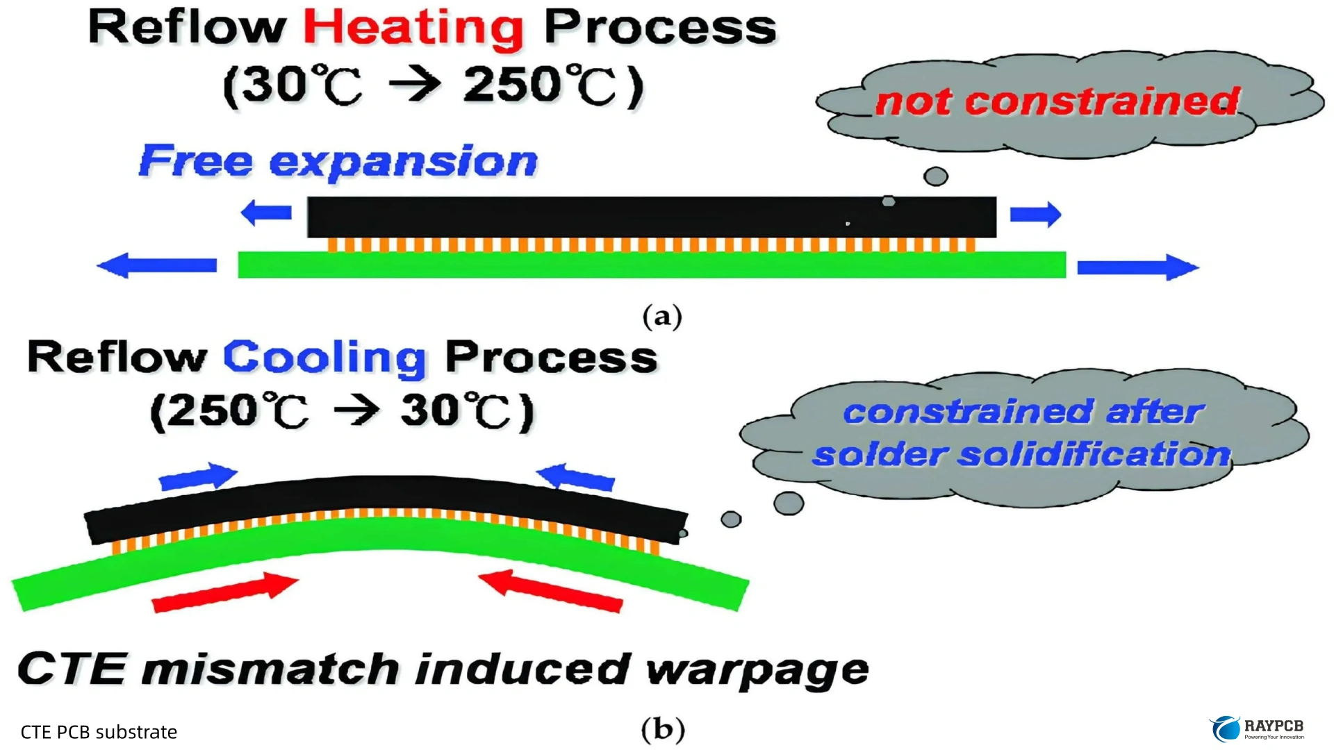
A single thermal excursion rarely causes catastrophic failure on its own. The real danger is thermal cycling โ€” repeated heating and cooling that accumulates mechanical stress in copper structures, solder joints, and substrate interfaces. Think of it like bending a paper clip back and forth: each cycle doesn’t break it, but eventually fatigue sets in.

Plated Through-Hole (PTH) Barrel Cracking

This is the classic CTE failure mode in multilayer boards. The Z-axis CTE mismatch between the copper plating (~17 ppm/ยฐC) and the FR-4 substrate (~55โ€“60 ppm/ยฐC) subjects PTH barrels to enormous cyclic strain. Every time the board heats up, the substrate expands far more than the copper barrel can accommodate. Over hundreds or thousands of cycles, this initiates cracks in the barrel wall โ€” often at the mid-span or at the interface with inner layers. The result is intermittent continuity that’s maddeningly difficult to reproduce at room temperature during debug.

High aspect ratio vias (typically 8:1 or greater) are especially vulnerable. Thicker plating or via-fill copper can mitigate the problem, but material selection remains the best first line of defense.

BGA and Surface Mount Solder Joint Fatigue

When a ceramic chip carrier (CTE โ‰ˆ 6 ppm/ยฐC) sits on standard FR-4 (CTE โ‰ˆ 15โ€“18 ppm/ยฐC in X/Y), every thermal cycle shears the solder joints. Large components like BGAs amplify this effect because corner joints must absorb the cumulative displacement over a larger footprint. The joints work-harden over time and eventually crack โ€” often beginning at the corner balls of a BGA array where the thermal displacement is greatest.

Lead-free solder alloys, now mandated in most markets, are actually less ductile than tin-lead solders, which makes CTE mismatch management even more critical than it was in the SnPb era.

Delamination and Pad Lifting

Extreme Z-axis expansion puts direct tensile stress on the bond between copper planes and the substrate resin. If absorbed moisture vaporizes rapidly during reflow (the “popcorn” effect), or if the thermal excursion approaches the glass transition temperature (Tg), this stress can physically separate the copper from the laminate. Pad lifting and inter-layer delamination are often terminal failure modes that render the board unrepairable.

The Role of Tg in CTE Behavior

Glass transition temperature (Tg) and CTE are deeply interconnected. Below Tg, a polymer-based substrate is in its rigid, glassy state โ€” CTE values are relatively controlled. Once the material crosses Tg, the resin transitions to a softer, rubbery state and the CTE โ€” especially in the Z-axis โ€” increases steeply. For standard FR-4, Tg is around 130ยฐC; high-Tg variants push this to approximately 170ยฐC.

The practical implication: if your board routinely operates near or above its substrate’s Tg, you’re running in a regime where Z-axis expansion accelerates sharply, dramatically increasing stress on vias and conductors. Lead-free reflow processes, which push temperatures to 250โ€“260ยฐC, briefly exceed the Tg of standard FR-4 during every assembly pass. This is why high-Tg laminates are now essentially the default for most production designs.

Note that Tg is reversible โ€” the material returns to its glassy state when it cools below Tg. Decomposition temperature (Td) is the point of irreversible chemical breakdown, which is typically above 300ยฐC for standard laminates. You never want to see Td during normal operation.

CTE Values for Common PCB Substrate Materials

Understanding how different substrate materials compare on CTE is essential before making a material selection decision. The table below consolidates typical values from published datasheets across commonly used PCB laminates.

Table 1: CTE Comparison of Common PCB Substrate Materials

MaterialX/Y CTE (ppm/ยฐC)Z-Axis CTE (ppm/ยฐC)Tg (ยฐC)Typical Use Case
Standard FR-411โ€“1855โ€“70130โ€“140General-purpose consumer/industrial
High-Tg FR-411โ€“1550โ€“65150โ€“175Industrial, multi-layer, lead-free assembly
Polyimide12โ€“1650โ€“60250โ€“260+Aerospace, flex, high-temperature
PTFE (Rogers, Taconic)17โ€“2424โ€“50โ€”RF, microwave, high-frequency
Rogers RO4350B11โ€“14~32>280 (Td)RF, cellular, radar
Ceramic (Alโ‚‚Oโ‚ƒ)6โ€“76โ€“7N/A (inorganic)Power electronics, high-reliability
Aluminum Nitride (AlN)4.3โ€“5.84.3โ€“5.8N/A (inorganic)High-power, LED, automotive
Copper (conductor)~17~17N/ATraces, planes, plating
Silicon (chip)~2.6~2.6N/ADie-level reference

Values are approximate and vary by manufacturer and specific grade. Always verify against laminate supplier datasheets for design sign-off.

The ceramic entries stand out immediately โ€” at 4โ€“7 ppm/ยฐC, they approach the CTE of silicon (~2.6 ppm/ยฐC), which is why ceramics are favored for bare-die mounting and power module applications where direct die-attach is involved. The flip side is that ceramic substrates are brittle, expensive, and require specialized manufacturing processes.

Substrate-Specific CTE Profiles: What Each Material Means in Practice

FR-4 and High-Tg FR-4

FR-4 remains the workhorse of the industry for very good reasons: it’s cost-effective, widely available, and well-characterized. But its Z-axis CTE of 55โ€“70 ppm/ยฐC demands respect. For boards with through-holes above 6:1 aspect ratios, multiple reflow cycles, or operating environments above 85ยฐC, consider upgrading to a high-Tg variant such as Isola IS410, Panasonic Megtron 6, or Isola FR408HR. These materials keep Tg in the 170โ€“190ยฐC range, giving you significantly more Z-axis dimensional stability through reflow.

Polyimide

Polyimide substrates (DuPont Kapton being the most recognized film) offer Tg values above 250ยฐC and Z-axis CTE of around 50โ€“60 ppm/ยฐC โ€” comparable to high-Tg FR-4 on the Z-axis, but with dramatically better performance at elevated temperatures. Polyimide is essentially the default for aerospace, military, and flex PCB applications. The trade-off is higher material cost and a tendency for moisture absorption, which requires pre-baking before assembly.

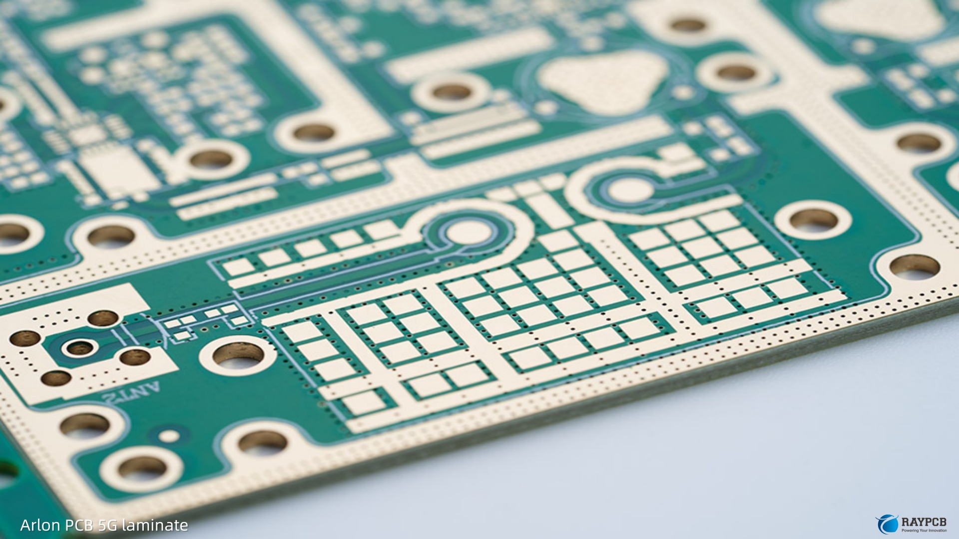
PTFE-Based Laminates (Rogers, Taconic, Isola)

PTFE (polytetrafluoroethylene) substrates offer excellent high-frequency properties โ€” low dielectric constant, stable Dk over temperature, and very low loss tangent. However, PTFE’s CTE behavior is more complex. While Z-axis CTE can be controlled with ceramic fillers (as in Rogers’ RO4000 series), pure PTFE tends toward higher X/Y CTE values, which complicates dimensional control during fabrication. The Rogers RO4350B specifically addresses this with a hydrocarbon-ceramic composition that delivers Z-axis CTE around 32 ppm/ยฐC while enabling standard FR-4 compatible processing. For designs requiring both RF performance and solid CTE management, Arlon PCB materials are another well-established option in the RF laminate space.

Ceramic Substrates

Alumina (Alโ‚‚Oโ‚ƒ) and aluminum nitride (AlN) ceramics deliver isotropic CTE values in the 4โ€“7 ppm/ยฐC range โ€” genuinely matched to silicon devices. Add thermal conductivity values of 20โ€“200 W/mK (compared to FR-4’s 0.3โ€“0.4 W/mK) and you have materials purpose-built for power electronics, high-brightness LEDs, and automotive modules where heat dissipation and component-substrate CTE compatibility are both critical constraints. The cost and specialized processing requirements mean ceramics remain reserved for demanding applications where FR-4 simply cannot meet the reliability targets.

CTE Mismatch Failure Modes: A Diagnostic Reference

When reviewing field failures or running reliability analysis, it helps to map symptoms directly to likely CTE-related root causes.

Table 2: CTE Failure Modes and Root Causes

Failure SymptomPrimary CTE DriverMost Likely Root Cause
PTH barrel cracksHigh Z-axis CTEFR-4 with >6:1 via aspect ratio, cycling above 85ยฐC
BGA corner ball openX/Y CTE mismatchCeramic component on FR-4; inadequate underfill
Via neck fracture (HDI)Z-axis CTE at TgOperating above Tg; insufficient resin content
Pad liftingZ-axis CTE + moistureMoisture-driven delamination during reflow
Solder joint fatigueX/Y CTE mismatchRepeated cycling, especially with large LCCCs
Delamination between layersZ-axis CTE at TgHigh Tg exceedance + absorbed moisture
Trace lifting on flexSubstrate CTE vs. copperPTFE or polyimide with poor adhesion prep

Design Strategies to Manage CTE PCB Substrate Stress

Material selection is the primary lever, but layout and manufacturing choices also matter significantly.

Symmetrical Stack-Ups

Asymmetric layer structures create unbalanced CTE-driven stress that can warp boards during reflow or over operational temperature swings. Mirror your stack-up โ€” match material types, copper weight, and prepreg thickness symmetrically about the board center. This is standard practice but still surprisingly often overlooked in fast-moving design cycles.

Via Design for Z-Axis CTE Management

For high-reliability designs, filled and capped vias significantly outperform unfilled barrels in thermal cycling. Copper via fill eliminates the differential between substrate expansion and hollow copper barrel expansion. For HDI designs specifically, choosing a laminate with a low-Z-axis CTE resin system is non-negotiable โ€” any resin that manages Z-axis expansion to below 50 ppm/ยฐC before Tg will substantially extend PTH fatigue life.

Underfill for BGA and Flip-Chip Components

Underfill epoxy โ€” applied beneath BGAs and flip-chip components โ€” distributes CTE-driven shear stress across the entire die footprint rather than concentrating it in corner solder balls. It’s an essential reliability tool for ceramic-packaged devices on FR-4 substrates. Select underfill materials with CTE values intermediate between the component and the substrate to avoid simply relocating the stress concentration.

Thermal Via Arrays and Copper Spreading

Strategic thermal via placement under high-power components reduces the temperature delta across the board, directly reducing the magnitude of CTE-driven dimensional changes. More uniform temperature distribution means less localized stress. Increasing copper weight in ground and power planes also improves thermal spreading, reducing hot spots that would otherwise drive elevated local CTE excursions.

Table 3: Design Mitigation Techniques vs. CTE Failure Mode

CTE Failure RiskRecommended MitigationPriority
PTH barrel cracking (high aspect ratio)Copper via fill; upgrade to high-Tg materialCritical
BGA solder joint fatigue (CTE mismatch)Underfill; CTE-matched substrate selectionHigh
Board warpage during reflowSymmetrical stack-up; controlled copper balanceHigh
Delamination in harsh environmentsLow Z-axis CTE resin; controlled Tg marginHigh
HDI via neck fracturesLow Z-axis CTE prepreg; limit reflow cyclesCritical
Trace lifting on PTFE boardsSurface preparation (plasma or chemical treatment)Medium

Measuring and Characterizing CTE: Differential Thermal Analysis

For anyone doing materials qualification or investigating field failures, Differential Thermal Analysis (DTA) or Thermomechanical Analysis (TMA) are the go-to techniques for measuring CTE and identifying Tg accurately. TMA is particularly useful because it directly measures dimensional change as a function of temperature, making it the most direct way to characterize the Z-axis CTE of a laminate sample. DTA detects the thermal events (including the glass transition) by measuring heat flow differences between a test sample and an inert reference.

If you’re qualifying a new laminate for a high-reliability program, don’t rely solely on datasheet values โ€” run TMA on your actual laminate lot. Variations in weave style, resin content, and fiber sizing between manufacturer batches can produce measurable CTE variation even within the same nominal grade.

Selecting the Right CTE PCB Substrate for Your Application

The table below maps common application categories to appropriate substrate choices, considering CTE requirements alongside other key parameters.

Table 4: Application-Driven Substrate Selection Guide

ApplicationKey CTE ConcernRecommended SubstrateNotes
Consumer electronicsModerate โ€” cost-drivenStandard FR-4Fine for limited thermal cycling
Industrial controlZ-axis, high cycle lifeHigh-Tg FR-4 (Tg 150โ€“170ยฐC)Lead-free assembly compatible
Automotive electronicsX/Y and Z-axis, -40 to 125ยฐCHigh-Tg FR-4 or polyimideAEC-Q standards often apply
Aerospace / DefenseAll axes, extreme rangePolyimideMIL-spec qualification common
RF / MicrowaveX/Y stability, Dk stabilityRogers RO4000 series / PTFECTE compatible with FR-4 processing (RO4350B)
LED lighting (high-power)Z-axis, heat dissipationMetal-core (MCPCB) or ceramicThermal conductivity priority
Power electronics / EVComponent-to-substrate matchCeramic (AlN, Alโ‚‚Oโ‚ƒ)Near-silicon CTE matching
Flexible / wearableDynamic flex cyclingPolyimide flexCTE must accommodate bending radius

Useful Resources for PCB Engineers

The following resources are worth bookmarking for substrate CTE data, design tools, and deeper technical reference:

Laminate Datasheets and Material Databases

Design and Reliability References

Learning and Technical Communities

Frequently Asked Questions About CTE PCB Substrate

What is a good CTE value for a PCB substrate?

For the X/Y plane, a CTE value between 11 and 18 ppm/ยฐC is typical for FR-4 class materials and generally compatible with copper conductors (~17 ppm/ยฐC). For the Z-axis, target below 70 ppm/ยฐC for standard designs and below 55 ppm/ยฐC for high-reliability or high-cycling applications. Ceramic substrates achieve 4โ€“7 ppm/ยฐC across all axes and offer the best match to silicon components, though at substantially higher cost.

Why does Z-axis CTE matter more than X/Y CTE?

The woven glass reinforcement in most rigid laminates constrains in-plane (X/Y) expansion significantly, keeping those values relatively close to copper. The Z-axis has no such reinforcement โ€” only the resin system governs out-of-plane expansion. Since plated through-holes run the full board thickness in the Z-direction, they experience the full impact of the substrate-copper CTE mismatch on every thermal cycle. This is why Z-axis CTE is typically 3โ€“5ร— higher than X/Y CTE in glass-weave laminates.

How does CTE relate to the glass transition temperature (Tg)?

Below Tg, a laminate’s CTE is relatively stable. As temperature rises through and above Tg, the resin softens and Z-axis CTE increases steeply โ€” in some materials more than doubling. This is why high-Tg materials are preferred for applications with elevated operating temperatures: they maintain tighter CTE control over a wider temperature range. Always select a substrate whose Tg is comfortably above the maximum expected operating temperature, with additional margin for reflow excursions.

Can I use standard FR-4 for automotive PCBs?

It depends on the specific application and the thermal cycling profile. Automotive under-hood electronics often see temperature swings from -40ยฐC to 125ยฐC or higher, which represents a demanding cycling environment. Standard FR-4 (Tg ~130ยฐC) would be borderline or insufficient for under-hood applications. High-Tg FR-4 (Tg 150โ€“170ยฐC) is more appropriate, and polyimide is the choice for the most demanding locations. The AEC-Q standard test protocols for automotive reliability are a useful guide for material qualification.

What is the best way to reduce CTE-related solder joint failures under BGAs?

The most effective combination is: (1) substrate selection to minimize the CTE delta between the component package and PCB โ€” for ceramic BGAs, consider a low-CTE laminate or a CTE-matched core material; (2) underfill application to distribute shear stress across the full component footprint; and (3) thermal management to reduce the temperature excursion during operation, thereby reducing the magnitude of differential expansion on every cycle. For very large ceramic packages on FR-4, underfill is essentially mandatory if the assembly must pass automotive or MIL-spec thermal cycling.

Understanding CTE PCB substrate behavior is one of the most practical reliability skills a PCB engineer can develop. It’s not glamorous, but it’s the kind of fundamental knowledge that separates boards that survive the field from those that don’t. Spec the right laminate, account for Z-axis expansion in your via design, and use underfill where the mismatch is severe โ€” and your products will thank you for it with fewer returns.

Bondply vs Prepreg: What’s the Difference in PCB Multilayers?

Learn the key differences in bondply vs prepreg PCB materials โ€” with comparison tables, stack-up examples, and selection guidance for RF, flex, and FR-4 multilayers.

If you’ve spent any time specifying materials for multilayer PCBs, you’ve almost certainly encountered both terms and possibly used them interchangeably. Don’t feel bad โ€” a lot of engineers do, and for standard FR-4 digital boards it rarely causes problems. But once you’re building high-frequency RF stacks, rigid-flex constructions, or boards where controlled impedance and signal loss genuinely matter, the distinction between bondply vs prepreg PCB materials becomes critically important.

This article walks through both materials from the ground up, explains exactly where they diverge, and gives you the practical decision framework to choose correctly for your next design.

Understanding the Basics: What Is Prepreg in PCB Manufacturing?

Prepreg โ€” short for pre-impregnated โ€” is a sheet of woven fiberglass cloth that has been saturated with partially cured resin, typically epoxy. “Partially cured” is the key phrase. Prepreg sits in what material scientists call the B-stage โ€” the resin has been processed enough to be handleable and non-tacky at room temperature, but it hasn’t completed its cure. That half-finished state is exactly what makes it useful. When you apply heat and pressure during lamination, the resin softens, flows into gaps, wets adjacent copper surfaces, and then fully cross-links into a rigid, permanently bonded dielectric layer.

In a standard multilayer rigid PCB, prepreg lives between the inner core layers, acting simultaneously as the adhesive that bonds the stack-up together and as the insulating dielectric that controls impedance between conductive layers. Take a 6-layer board: you likely have two inner cores (each double-sided) and prepreg sheets filling the spaces between them and the outer copper foils. Without prepreg, you don’t have a multilayer board.

The Three Grades of Prepreg You’ll See on Datasheets

Prepreg is classified by resin content, and this affects both thickness and electrical properties. The three categories you’ll encounter are:

Standard Resin (SR): Lower resin content, approximately 35โ€“45%. Thinner finished laminate with higher glass content. Relatively stable Dk but less void-fill capability.

Medium Resin (MR): Balanced resin content around 45โ€“55%. The general-purpose choice for most multilayer designs.

High Resin (HR): Resin content above 55%. Flows more during lamination, better for filling high-copper-density inner layers. Tends to have higher Dk due to greater resin proportion.

Most fabricators default to one or two prepreg grades for standard FR-4 work, but for controlled impedance layers you should be actively specifying โ€” the Dk variation between SR and HR of the same glass style can be meaningful at high frequencies.

What Is Bondply? Clearing Up the Confusion

This is where most explanations fall short. “Bondply” is not simply another word for prepreg โ€” it describes a specific class of bonding materials that are unreinforced, meaning they contain no woven glass fabric at all. In the most common form, a bondply is a thin-film adhesive sheet: pure resin, no fiber scaffold.

The distinction matters because the glass weave is what gives standard prepreg its mechanical rigidity in the X/Y plane and largely controls its in-plane dimensional stability. Strip that out and you get a material with fundamentally different mechanical and electrical behavior.

Bondply in Rigid High-Frequency PCBs

The best-known rigid bondply product is the Rogers 2929 Bond Sheet. It’s a non-reinforced, hydrocarbon-based thermoset film available in thicknesses of 1.5, 2, and 3 mils (0.038โ€“0.076 mm). Its primary purpose is bonding multilayer stacks made from PTFE-based laminates โ€” materials like Rogers RT/duroid 6000 or RO3000 series that are notoriously difficult to bond with standard epoxy prepreg.

Why can’t you just use FR-4 prepreg to bond PTFE boards? Because PTFE surfaces are chemically inert โ€” standard epoxy resin doesn’t adhere to them reliably. The 2929 bondply uses a proprietary cross-linked resin chemistry specifically formulated to wet and bond PTFE composite surfaces, while still delivering a low Dk of 2.9 and loss tangent below 0.003 at 10 GHz. That means the bondply layer doesn’t degrade the high-frequency performance you’re designing the PTFE laminate to deliver in the first place.

Bondply in Flex and Rigid-Flex PCBs

In the flex and rigid-flex world, bondply has a different but equally specific role. Here, bondply typically consists of a polyimide film core coated on both sides with B-staged acrylic adhesive. It’s used to bond copper-clad flex laminate (FCCL) layers together in multilayer flex constructions โ€” essentially doing the same job that prepreg does in a rigid board, but using an unreinforced polyimide-adhesive sandwich instead of a glass-epoxy sheet.

The reason you don’t use woven-glass prepreg in flex circuits should be obvious: glass weave doesn’t bend. A flex circuit that incorporates fiberglass reinforcement in its flex regions isn’t really a flex circuit โ€” it’s a badly designed rigid board. Bondply provides the inter-layer dielectric and adhesion without compromising the flex zone’s ability to bend, fold, or articulate.

Bondply vs Prepreg PCB: The Core Differences Side by Side

With both materials defined properly, the comparison becomes much clearer.

Table 1: Bondply vs Prepreg โ€” Fundamental Differences

PropertyStandard PrepregBondply
ReinforcementWoven fiberglass clothNone (unreinforced film)
Resin systemEpoxy (FR-4); ceramic-loaded epoxy (RF grades)Hydrocarbon thermoset (rigid RF); Acrylic (flex)
Primary applicationRigid multilayer FR-4; RF prepreg variantsPTFE/RF multilayer bonding; flex/rigid-flex
FlexibilityRigid after cureRigid (thermoset) or flexible (polyimide/acrylic)
Typical thickness2โ€“8 mils (0.05โ€“0.2 mm)1.5โ€“5 mils (0.038โ€“0.127 mm)
Dielectric constant (Dk)3.5โ€“4.5 (FR-4 grades); 3.2โ€“3.5 (RF grades)2.9 (Rogers 2929); varies by product
Loss tangent (Df)0.015โ€“0.025 (FR-4); 0.003โ€“0.005 (RF grades)<0.003 (Rogers 2929)
Dimensional stability (X/Y)High โ€” glass restrains in-plane expansionLower โ€” no glass fiber constraint
Via fill capabilityGood (standard flow)Excellent (controlled flow, blind via filling)
Compatible laminate systemsFR-4 cores; Rogers RO4000 (RO4450B/F variants)PTFE, RO3000, RT/duroid, flex polyimide cores
ProcessingStandard FR-4 press parametersSpecific press temperatures; autoclave compatible

Table 2: Prepreg Grades for Common FR-4 Applications

Glass StyleNominal Thickness (mil)Resin ContentTypical Dk at 1 GHzCommon Use
1062โ€“3HR (65โ€“72%)3.8โ€“4.0Fine pitch HDI; thin dielectrics
10802.5โ€“3.5MR (55โ€“65%)3.9โ€“4.1General multilayer; outer layers
21164โ€“5MR (45โ€“55%)4.0โ€“4.2Standard inner layers; impedance-controlled
76286โ€“8SR (35โ€“45%)4.2โ€“4.4Thick build-ups; structural plies

Values approximate; verify against specific laminate supplier datasheets. Dk shifts with resin content.

Where the Confusion Comes From โ€” and Why It Matters

Part of the reason “bondply” and “prepreg” get conflated is that both materials occupy the same position in a stack-up โ€” the inter-layer bonding position โ€” and both are technically B-stage materials that cure under heat and pressure. Some vendors also loosely call their bondply products “bondply prepreg” which doesn’t help.

The confusion is harmless if you’re building a standard FR-4 board. But it becomes a real problem in three scenarios:

Scenario 1 โ€” RF/Microwave Multilayers: If you specify “prepreg” on a drawing for a PTFE-based RF multilayer without specifying bondply, a fabricator using standard epoxy prepreg to bond PTFE cores may give you a board with delamination risk and degraded high-frequency insertion loss. The Dk mismatch between a standard FR-4 prepreg layer and surrounding PTFE laminates also disrupts impedance continuity through the stack.

Scenario 2 โ€” Flex and Rigid-Flex Constructions: Using woven-glass prepreg in flex zones will kill the flex functionality and introduce crack initiation sites at glass fiber/resin boundaries under repeated bending. Flex designs must specify bondply (polyimide/acrylic) in all dynamically flexed regions.

Scenario 3 โ€” Blind and Buried Via Designs: For designs requiring tight tolerance cavity cutback ratios (used in buried cavity constructions), the controlled flow characteristics of bondply products like Rogers 2929 are specifically engineered for predictable material pullback during routing. Standard prepreg’s flow behavior is less tightly controlled for this purpose.

How Bondply and Prepreg Affect Electrical Performance

Signal integrity engineers need to pay attention to how these bonding layers influence Dk, loss tangent, and impedance control โ€” especially as signal speeds push into multi-gigabit territory.

Dielectric Constant Stability

Standard FR-4 prepreg Dk varies more with resin content and processing conditions than the laminate core because it starts out as a B-stage material with variable flow. Core materials from the same manufacturer in the same grade typically hold Dk to within ยฑ5%; prepreg can vary ยฑ10% before fabrication. This is why impedance modeling tools require you to specify prepreg style (1080, 2116, 7628) explicitly โ€” the Dk delta between glass styles is real and significant at controlled impedance.

Bondply like Rogers 2929, because it’s unreinforced, delivers more uniform Dk across the bonding layer (no glass/resin heterogeneity), but its isotropic nature also means no fiber-induced anisotropy โ€” which is actually an advantage for RF designs where you want predictable, direction-independent electrical behavior.

Loss Tangent and Insertion Loss

This is the biggest performance differentiator at high frequencies. Standard FR-4 prepreg has a loss tangent of 0.015โ€“0.025 at 1 GHz โ€” acceptable for digital signals below 10 Gbps, but increasingly painful as frequencies rise. Rogers RO4450B/F prepreg (the glass-reinforced RF prepreg variant) drops this to around 0.004. Rogers 2929 bondply achieves below 0.003 at 10 GHz, making it among the lowest-loss bonding materials commercially available for multilayer RF construction.

If you’re designing a phased array antenna, automotive radar module, or 5G mmWave board and you’re bonding your RF laminates with standard FR-4 prepreg because it was in stock, you’re introducing unnecessary insertion loss in exactly the interlayer regions you need the signal to traverse cleanly.

Practical Material Selection: When to Use Which

The decision tree is actually straightforward once you understand the underlying purpose of each material.

Table 3: Application-Driven Selection Guide โ€” Bondply vs Prepreg

Application TypeBonding Material ChoiceReason
Standard FR-4 digital multilayerFR-4 prepreg (2116 or 7628)Cost-effective; compatible; adequate for digital speeds
High-speed digital (>10 Gbps)Low Dk/Df prepreg (e.g., Megtron 6 PP, Isola I-Tera)Reduced insertion loss vs standard FR-4 prepreg
RF/microwave multilayer on PTFERogers 2929 bondplyRequired for PTFE adhesion; maintains low Dk/Df
RF multilayer on RO4000 seriesRogers RO4450B or RO4450F prepregFR-4 compatible processing; ceramic-filled, low loss
Rigid-flex PCB (flex zones)Polyimide bondply (e.g., DuPont, Panasonic)No glass reinforcement; maintains flex capability
Rigid zones in rigid-flexFR-4 prepreg or high-Tg prepregSame as standard rigid board in stiffened areas
HDI / blind via build-upThin prepreg (106 or 1080 HR)Controlled thickness; adequate resin fill
Buried cavity constructionsBondply (controlled flow)Predictable cutback ratios; blind via fill capability
Arlon-based RF multilayersArlon bondply/prepreg variantsArlon PCB materials require matched bonding systems for optimum high-frequency performance

Stack-Up Construction: How Bondply and Prepreg Appear in Real Designs

Understanding where these materials sit in a physical stack-up clarifies why their selection matters.

Table 4: Typical 4-Layer Stack-Up Examples Using Both Material Types

Layer PositionStandard Digital (FR-4)RF Multilayer (PTFE + Rogers 2929)
Top copper (L1)1 oz Cu foil1 oz Cu foil
Bonding layer (L1โ€“L2)FR-4 prepreg (2116)Rogers 2929 bondply
Core (L2โ€“L3)FR-4 core 0.8 mmRO4003C or RT/duroid core
Bonding layer (L3โ€“L4)FR-4 prepreg (2116)Rogers 2929 bondply
Bottom copper (L4)1 oz Cu foil1 oz Cu foil

For rigid-flex, the flex zone replaces the core with FCCL (flexible copper-clad laminate) and substitutes polyimide bondply for the prepreg layers in the dynamic bend region, while maintaining standard prepreg in the stiffened rigid zones.

Fabrication Considerations You Should Know

A few processing points that affect how you specify these materials:

Press parameters differ significantly. Standard FR-4 prepreg cures at around 170โ€“185ยฐC under flat-bed press conditions. Rogers 2929 bondply requires a lamination temperature of approximately 475ยฐF (246ยฐC). If your fabricator doesn’t have process documentation for the bondply you’ve specified, push back โ€” incorrect press cycles are a primary cause of delamination in RF multilayer builds.

Bondply films often ship with a carrier film. The releasable carrier on materials like Rogers 2929 protects the adhesive surface during handling, conductive paste screening, and booking operations. This carrier is removed before final lamination. It also allows the bondply to be pre-laminated to an inner core for simultaneous routing โ€” meaning the bondply and core can be slotted together in a single CNC operation, which matters for buried cavity designs.

Moisture sensitivity varies. Polyimide flex bondplies are hygroscopic and typically require pre-baking (typically 4โ€“8 hours at 110โ€“125ยฐC) before lamination to prevent moisture-driven delamination during the high-pressure cure cycle. Standard FR-4 prepreg also benefits from controlled storage humidity but is generally more forgiving than polyimide-based systems.

Useful Resources for PCB Engineers

Engineers working with bondply and prepreg materials will find the following references worth bookmarking:

Manufacturer Datasheets and Product Selectors

Standards and Design References

Technical Learning

Frequently Asked Questions: Bondply vs Prepreg PCB

Is bondply the same as prepreg?

Not exactly. All bondplies function as bonding materials, and they are technically B-stage materials like prepreg, but the defining difference is that bondply is unreinforced โ€” it contains no woven fiberglass. Standard prepreg contains a glass-fiber scaffold saturated with resin. This structural distinction drives differences in flexibility, dimensional stability, Dk behavior, and compatibility with different laminate systems. The term “bondply” is sometimes used loosely to describe any thin bonding film, so always check the datasheet to confirm whether a material is reinforced or unreinforced.

Can I use FR-4 prepreg to bond PTFE-based RF laminates?

Generally, no โ€” not reliably. PTFE surfaces are chemically inert and standard epoxy-based FR-4 prepreg does not develop adequate adhesion to them. The bond may appear adequate initially but often fails under thermal cycling or elevated temperature exposure. For PTFE-based multilayers (RT/duroid, RO3000 series), use a bondply specifically formulated for PTFE bonding, such as Rogers 2929. For the RO4000 series (which uses ceramic-hydrocarbon chemistry rather than pure PTFE), Rogers RO4450B or RO4450F prepreg is the appropriate choice and is compatible with standard FR-4 press processes.

What bondply should I use in rigid-flex PCB designs?

In the dynamically flexed regions of a rigid-flex board, specify a polyimide-based bondply with acrylic or low-flow adhesive โ€” DuPont Pyralux bondply is a common choice. These materials maintain the flex capability by avoiding glass reinforcement. In the stiffened (rigid) zones, standard FR-4 prepreg or high-Tg prepreg is appropriate, just as in an all-rigid multilayer. Your stack-up drawing should clearly differentiate bonding materials between flex and rigid zones to prevent fabrication errors.

How does prepreg choice affect controlled impedance?

Significantly. The dielectric constant of the prepreg layer determines the impedance of conductors referenced to it. Different glass styles (106, 1080, 2116, 7628) have different Dk values, and even within the same style, HR vs SR prepreg shifts Dk because more resin means lower glass/resin ratio and lower effective Dk. For any controlled impedance layer, specify the exact prepreg style and resin content to your fabricator, verify their stack-up model against your impedance target, and request coupons for TDR validation on the first article.

What’s the difference between Rogers 2929 bondply and Rogers RO4450B prepreg?

Both are used to bond RO4000 series multilayers, but they’re different materials. RO4450B is a glass-reinforced ceramic-hydrocarbon prepreg โ€” it has woven glass cloth, Dk of approximately 3.3โ€“3.5 at 10 GHz, and processes similarly to FR-4. Rogers 2929 is an unreinforced hydrocarbon thermoset film with Dk of 2.9 and loss tangent below 0.003. The 2929 is lower loss and thinner (down to 1.5 mil), making it preferable for very high-frequency designs and for bonding PTFE-based materials where glass-reinforced prepreg won’t adhere. RO4450B is better suited to designs where FR-4-compatible processing is required and where the slightly higher Dk is acceptable.

Getting the bondply vs prepreg question right from the start of your design is cheaper than a delamination investigation after first article. If you’re in the RF or flex space, your laminate choice and your bonding material choice need to be made together โ€” they’re two sides of the same multilayer equation.

Arlon AD Bondply: The Complete Guide to Bonding High-Frequency PTFE Laminates in Multilayer PCBs

Learn how Arlon AD bondply bonds high-frequency PTFE laminates in multilayer PCBs โ€” grades, stackup design, lamination parameters, and FAQs for RF engineers.

If you’ve ever tried to build a multilayer RF board using PTFE-based laminates, you already know the headache. PTFE doesn’t bond like FR-4. It flows differently, expands differently, and if you try to laminate it using standard epoxy prepreg, you end up with either mismatched dielectric properties or delamination failures down the road. That’s exactly where Arlon AD bondply enters the picture โ€” and for engineers working on base station antennas, phased array radars, or 5G infrastructure boards, understanding this material properly can be the difference between a first-pass success and a very expensive stack of scrap.

This guide covers everything you need to know: what the AD Series actually is, how its bonding plies work, how to select the right grade for your stackup, and practical tips on multilayer lamination processing. Whether you’re designing a hybrid RF/digital board or an all-PTFE microwave structure, let’s dig in.

What Is the Arlon AD Series? Understanding the PTFE Composite Foundation

<invoke name=”places_search”> <invoke name=”web_search”>

The Arlon AD Series is a family of woven fiberglass-reinforced PTFE composite laminates engineered specifically for printed circuit board substrates in high-frequency applications. What makes it unique compared to traditional PTFE-only substrates is the deliberately higher fiberglass-to-PTFE ratio. This design choice trades a small amount of raw electrical performance for a significant improvement in dimensional stability โ€” something that matters enormously when you’re trying to hold tight impedance tolerances across a multilayer panel.

Arlon’s Electronic Materials Division (EMD), based in Rancho Cucamonga, California, has been producing PTFE-based microwave laminates for over 50 years. The AD product line sits within their microwave materials portfolio alongside CuClad, DiClad, CLTE, and AD1000 series materials, covering dielectric constants from roughly 2.17 up to 10.2.

For the AD Series specifically, dielectric constants range from 2.5 to 3.5, available in dielectric thicknesses from 0.015″ to 0.062″, with custom thicker options available on request. The full lineup covers multiple Dk targets suited to different transmission line geometries and frequency bands.

Key Electrical Attributes of the AD Series

The core electrical appeal of the AD Series is the combination of low loss tangent and stable dielectric constant across a broad frequency range โ€” two things that PTFE does exceptionally well compared to FR-4 or standard epoxy laminates.

PropertyTypical ValueTest Method
Dielectric Constant (Dk)2.5 โ€“ 3.5 (grade-dependent)IPC-TM-650 2.5.5.5 / FSR
Loss Tangent (Df)0.0014 โ€“ 0.003IPC-TM-650 2.5.5.5
Z-axis CTELower than standard PTFEIPC-TM-650 2.4.24
Water Absorption< 0.1%IPC-TM-650 2.6.2
Copper Peel StrengthStandard ED / RTF foilIPC-TM-650 2.4.8

These numbers put the AD Series comfortably ahead of FR-4 (Df typically 0.018โ€“0.025) and broadly in line with competitive PTFE/glass materials from Rogers and Taconic โ€” though specific loss tangent values vary significantly between AD grades.

The AD Series Lineup: Choosing the Right Grade

Not all AD grades are the same. Over the years Arlon has expanded and refined the lineup, introducing ceramic-filled variants (designated with the “A” suffix) that offer even better thermal stability and lower loss. Here’s a practical breakdown:

AD Series Grade Comparison

GradeDk (Nominal)Key FeatureBest Use Case
AD2502.50PTFE/glass, cost-optimizedAntenna substrates, combiner boards
AD255A2.55Ceramic + PTFE + glass, very low Df (0.0014)Base station, high-gain antenna
AD260A2.60Ceramic-filled, tight Dk tolerance, FSR testedTelecom infrastructure, feed networks
AD3003.00Standard PTFE/glass, balanced Dk/costStripline, general microwave
AD300A3.00Ceramic-loaded, improved CTE vs AD300Hybrid multilayer stackups
AD320A3.20 ยฑ 0.04Ceramic, stable to 40 GHzmmWave, 5G, radar, medical imaging
AD350A3.50Ceramic-filled, higher DkMiniaturized circuits, filters
AD100010.2Ultra-high Dk ceramic/PTFEMiniaturization, patch antennas

The “A” designation โ€” visible in AD255A, AD260A, AD300A, AD320A โ€” signals the inclusion of micro-dispersed ceramic filler. This makes a real difference in practice. The ceramic loading reduces the coefficient of thermal expansion (CTE) in the Z-axis, bringing it closer to the expansion rate of copper. The result is improved plated through-hole (PTH) reliability, especially important in multilayer assemblies that see thermal cycling during assembly and field use.

Arlon uses the IPC TM-650 2.5.5.6 (FSR) test method on every panel for the ceramic-filled grades to guarantee dielectric constant consistency โ€” not just statistical sampling. For production PCBs where impedance tolerance is held to ยฑ5% or tighter, that per-panel testing matters.

What Is Arlon AD Bondply and Why Does It Exist?

Here’s where many PCB engineers get tripped up. When you build a multilayer board using AD Series cores, you can’t just sandwich them together with standard FR-4 prepreg and call it a day. The mismatch in dielectric properties and CTE between an epoxy prepreg and a PTFE core would undermine your impedance calculations and create a mechanical weak point at the bond interface.

Arlon AD bondply refers to the bonding ply materials โ€” low-density, resin-rich versions of the same PTFE-based material family โ€” used to join AD Series cores in a multilayer stackup. Arlon supplies copper-clad laminates together with bonding plies and prepregs specifically formulated to maintain electrical continuity and mechanical integrity between layers.

The concept parallels what Rogers does with their 2929 bondply for RO3000 and RT/duroid series laminates: rather than using a dissimilar adhesive, you bond like-with-like. A bonding ply derived from the same PTFE composite system will have compatible Dk, Df, CTE, and thermal processing characteristics, preserving signal integrity across layer boundaries.

Three Bonding Methods for PTFE Multilayer PCBs

Understanding Arlon AD bondply requires understanding where it fits in the broader landscape of PTFE bonding approaches. There are fundamentally three methods used in industry:

MethodMaterial UsedAdvantagesLimitations
Thermoplastic bonding filmsFEP, CTFE, or PTFE filmsLowest electrical lossHigh process temperature; not suited for sequential lamination
Thermoset prepreg / bondplyArlon AD bondply, Rogers 2929Sequential lamination capable; higher layer countSlightly higher Df than thermoplastic films
Fusion (direct) bondingNo adhesive โ€” direct PTFE-to-PTFEMaximum electrical uniformityRequires very high pressure (>1000 PSI), specialized press; challenging registration

The AD bondply approach falls into the thermoset/bondply category. It provides a middle path: better electrical properties than an epoxy prepreg, while being far more manufacturable than fusion bonding, which demands specialized induction heating press equipment and rigid process control.

For the majority of commercial wireless infrastructure boards โ€” base station combiners, antenna feed networks, power dividers โ€” the AD bondply approach offers the right compromise of performance, yield, and cost.

Multilayer Stackup Design with Arlon AD Bondply

Hybrid vs. All-PTFE Stackups

One of the most common real-world scenarios is the hybrid stackup: RF/microwave layers using AD Series cores, combined with lower-cost digital or power layers using FR-4 or mid-loss thermoset materials. This is economically attractive but introduces engineering challenges.

The primary concern is CTE mismatch. AD Series laminates, particularly the ceramic-filled “A” grades, have significantly lower CTE than standard FR-4. Under thermal cycling, differential expansion can stress the plated through-holes and cause barrel cracking or pad lifting. The AD bondply layer helps manage this transition, but the designer still needs to:

  • Keep high-frequency signal layers together in the stackup (avoid crossing the PTFE/FR-4 boundary with critical RF signals)
  • Size via drill diameters and aspect ratios conservatively for PTH zones that span both material types
  • Discuss the stackup with the fabricator early โ€” most shops that handle hybrid PTFE boards have proprietary lamination cycles optimized for specific material pairings

All-PTFE Stackup Considerations

For pure AD Series multilayers using AD bondply throughout:

  • The bonding ply is a lower-density version of the core material, allowing it to flow into trace gaps under heat and pressure during lamination
  • A general rule of thumb in the industry: use 5 mil bondply for every 1 oz of inner-layer copper to ensure adequate encapsulation around etched features
  • Lamination pressure requirements are higher than standard FR-4 โ€” typically exceeding 1000 PSI โ€” and dwell time must be controlled carefully to bring the bondply to full cure without thermal overshoot
  • PinLess lamination methods, commonly used for FR-4 multilayers, are problematic with PTFE because the standard spot-welding step requires very high local temperature and pressure that most welding machines can’t reliably deliver to PTFE. Pinned tooling or specialized induction welding equipment is typically required

Sample AD-Series Hybrid Stackup

LayerMaterialRole
L1AD260A (0.020″)RF signal layer โ€” microstrip
BondAD bondplyInter-layer adhesive
L2โ€“L3AD260A (0.031″)Ground / power plane
BondAD bondplyInter-layer adhesive
L4AD260A (0.020″)RF signal layer โ€” stripline
TransitionLow-flow thermoset prepregCTE buffer toward FR-4
L5โ€“L8High-Tg FR-4Digital / control layers

The key principle: keep RF signal layers grouped within the AD Series zone, and use a controlled-flow transition prepreg when moving to the FR-4 region.

Processing Guidelines for Arlon AD Bondply

If you’re working with a contract manufacturer, making sure they have hands-on experience with PTFE-based multilayers is non-negotiable. Here are the main process parameters to confirm:

Inner Layer Preparation

PTFE-based laminates require a sodium naphthalene (sodium etch) or similar chemical treatment, or a plasma activation process, on the bond surfaces before lamination. Standard oxide or micro-etch surface treatments used for FR-4 are insufficient โ€” they won’t provide adequate adhesion to the bondply. Skipping this step is a common root cause of delamination failures in the field.

Lamination Cycle

Typical parameters for AD bondply lamination (confirm with Arlon’s process guidelines for your specific grade):

ParameterTypical Range
Pressure800 โ€“ 1200 PSI
Peak Temperature350ยฐC โ€“ 380ยฐC (for PTFE-based bondply)
Vacuum Level< 10 mbar
Temperature Ramp Rate2โ€“5ยฐC/min to cure zone
Dwell Time at Peak30โ€“60 min

Note that these cycles are substantially more aggressive than standard FR-4 lamination (typically 175โ€“185ยฐC, 300โ€“500 PSI). Make sure your press, caul plates, and tooling are rated for these conditions.

Drilling and Through-Hole Plating

PTFE is soft and gummy compared to FR-4. Dull drill bits will smear PTFE into the hole wall, creating a contaminated surface that resists copper adhesion in the plating step. Use sharp, fresh drill bits, reduce drill speed or feed rate per the laminate manufacturer’s guidelines, and consider plasma de-smear rather than permanganic de-smear for PTFE-rich stackups.

Applications: Where Arlon AD Bondply Earns Its Keep

Engineers reach for Arlon AD bondply when the application demands both high-frequency electrical performance and the structural integrity of a multilayer PCB. Typical use cases include:

  • 5G base station antennas and feed networksย โ€” where low insertion loss and tight impedance control at 28 GHz and above are critical
  • Phased array radar systemsย โ€” where phase consistency across dozens of parallel signal paths demands a substrate with stable, predictable Dk over temperature
  • Satellite communication transpondersย โ€” operating at Ka-band and higher, where every 0.1 dB of loss matters
  • Medical imaging systemsย (MRI, ultrasound electronics) โ€” high-frequency signal integrity combined with reliability requirements
  • Power amplifier boardsย for wireless infrastructure โ€” where both RF performance and thermal management (enhanced by the ceramic filler’s higher thermal conductivity) are needed simultaneously

For Arlon PCB fabrication services that can handle these demanding stackups, partnering with a manufacturer who stocks Arlon materials and has established process qualification is strongly recommended.

Arlon AD Series vs. Competitive Materials

For context, here’s how the AD Series positions against other commonly specified high-frequency substrates:

MaterialDkDf (@10 GHz)CTE Z-axisProcessability
Arlon AD260A2.60~0.002Low (ceramic-loaded)Standard PTFE process
Arlon AD320A3.200.0032Low (ceramic-loaded)Standard PTFE process
Rogers RT/duroid 58802.200.0009ModerateRequires careful handling
Rogers RO4350B3.480.0037LowNear FR-4 processability
Taconic TLY-52.170.0009ModeratePTFE standard process
Standard FR-44.2โ€“4.80.018โ€“0.025HighEasiest, lowest cost

The AD Series “A” grades occupy a compelling middle ground: better loss performance than RO4350B (which is a thermoset, not PTFE), and far better dimensional stability and PTH reliability than glass-only PTFE laminates like RT/duroid 5880.

Useful Resources for Engineers

ResourceDescriptionLink
Arlon AD Series DatasheetOfficial electrical and mechanical properties for all AD gradesarlonemd.com
Arlon Microwave & RF Materials GuideComprehensive laminate selector covering all Arlon microwave productsAvailable via Arlon EMD or authorized distributors
IPC-4103IPC standard for high-speed/high-frequency base materialsipc.org
IPC-TM-650 Test MethodsStandard test methods for Dk, Df, CTE, peel strengthipc.org/TM
Arlon Laminate Guide PDFTechnical guide covering dielectric selection, loss, and multilayer designarlonemd.com/wp-content/uploads/2020/05/Laminate-Guide.pdf
AD Series PDF DatasheetArlon’s official AD Series product sheet with Dk vs. frequency curvescirexx.com/wp-content/uploads/AD-Series.pdf
RayPCB Arlon PCB ResourceFabrication guidance and Arlon material overview for PCB productionraypcb.com/arlon-pcb

Frequently Asked Questions (FAQs)

Q1: Can I use standard epoxy prepreg to bond Arlon AD Series cores in a multilayer?

You can, but it’s generally not recommended for RF-critical layers. Standard epoxy prepreg has a much higher loss tangent (Df ~0.018โ€“0.025 vs. ~0.002 for AD bondply) and a higher, mismatched CTE. For hybrid boards where only some layers are RF-sensitive, low-flow thermoset prepregs can be used as a transition layer between the PTFE zone and the FR-4 zone, but they should not sit directly adjacent to a critical RF signal layer if performance matters.

Q2: What’s the difference between Arlon AD bondply and Rogers 2929 bondply?

Both serve the same function โ€” bonding PTFE-based multilayer laminates โ€” but they’re chemically different systems from competing manufacturers. Rogers 2929 is a non-reinforced hydrocarbon-based thin-film adhesive (Dk ~2.9, Df <0.003), optimized for bonding RT/duroid and RO3000 series laminates. Arlon AD bondply is matched to the AD Series PTFE/ceramic composite family. While cross-manufacturer use is sometimes done in hybrid situations, best practice is to use the bondply from the same material family as your cores to ensure consistent Dk and CTE throughout the stackup.

Q3: What pressing equipment is required for AD bondply lamination?

AD bondply lamination requires a press capable of achieving 800โ€“1200 PSI at temperatures up to 380ยฐC under vacuum (<10 mbar). Conventional hydraulic flat presses equipped with high-temperature platens and a suitable vacuum system are commonly used. More recently, induction heating press systems (such as InduBond X-Press) have shown advantages for PTFE multilayers because they deliver uniform heat through stainless steel separators, reducing thermal gradients across the lamination book. For pin registration during layup, a pinned fixture system is recommended since spot-welding PTFE with standard PinLess welding machines is unreliable.

Q4: How does the ceramic filler in AD “A” grades affect bonding performance?

The micro-dispersed ceramic in grades like AD260A and AD320A serves two roles relevant to bonding. First, it reduces the Z-axis CTE to a value closer to copper’s expansion coefficient, which directly improves PTH barrel reliability during the thermal cycles of assembly and field use. Second, the ceramic loading improves dimensional stability in X-Y, reducing registration errors in high layer count builds. From a bondply perspective, the ceramic-filled core and the matching ceramic-filled bondply create a more uniform, homogeneous lamination that behaves predictably during repeated thermal cycling.

Q5: Is Arlon AD Series compatible with lead-free (Pb-free) assembly processes?

Yes, the AD Series and its bonding plies are compatible with lead-free soldering profiles. The ceramic-filled grades have decomposition temperatures well above the peak reflow temperatures required for SAC305 solder (typically 260ยฐC peak). However, because PTFE-based substrates have lower CTE than FR-4, the cumulative strain on PTH barrels during lead-free reflow (which reaches higher peak temperatures than SnPb reflow) should be evaluated carefully, particularly for high-aspect-ratio vias. Using the ceramic-filled “A” grades, which have lower Z-axis CTE, mitigates this risk significantly compared to non-ceramic PTFE laminates.

Summary: When to Specify Arlon AD Bondply

As a PCB engineer, the decision to use Arlon AD bondply comes down to a few key questions: Is your board operating above 3 GHz where FR-4 loss becomes significant? Are you building a multilayer stackup where at least some layers need to be PTFE-based? Do you need the multilayer to survive assembly and thermal cycling without delamination or PTH failures?

If the answer to all three is yes, the AD Series โ€” and specifically the ceramic-filled “A” grades โ€” paired with their matched bonding plies, gives you a well-supported, industrially proven path to a high-performance, manufacturable multilayer. The material is backed by 50+ years of Arlon’s microwave laminate expertise, broad industry familiarity among RF PCB fabricators, and a solid documentation ecosystem that makes qualifying a new process straightforward.

The engineering tradeoff is real: PTFE processing is more demanding and more expensive than FR-4. But for anything running at microwave frequencies where insertion loss, phase stability, and impedance precision matter, the AD Series is a genuine workhorse material โ€” and the bondply is what makes multilayer construction with it actually practical.

Arlon PTFE Laminates for Satellite & Space-Grade PCBs

Complete guide to Arlon PTFE space PCB laminates for satellite hardware โ€” covering CLTE-XT, CuClad, outgassing compliance (ASTM E595), thermal cycling, the 19ยฐC phase transition, and multilayer stack-up design for space-grade reliability.

Space is the most unforgiving operating environment a PCB will ever face. There are no service technicians 400 km above the Earth, no second chances when a satellite’s payload electronics fail mid-mission, and no way to rework a board that’s experienced delamination after 5,000 thermal cycles between -150ยฐC and +150ยฐC. When an Arlon PTFE space PCB fails, the mission fails โ€” and missions cost hundreds of millions of dollars.

This is exactly why the material decisions engineers make during the design phase matter so much in satellite and space applications. The laminate you specify will spend 15+ years in vacuum, absorb cosmic radiation, cycle through extreme temperature swings every 90 minutes in low Earth orbit, and never once be touched for inspection or repair. The physics of that environment demand a completely different set of material requirements than any terrestrial RF or commercial wireless design.

Arlon โ€” operating for over 50 years in PTFE-based microwave laminates and now part of Rogers Corporation โ€” has built a portfolio of PTFE and ceramic-filled PTFE materials specifically suited to these demands. This guide covers what space-grade PCB material requirements actually look like, which Arlon PTFE laminates address them, how CLTE, CLTE-XT, CuClad, and the QM100 cyanate ester family fit into different space electronics applications, and what engineers need to know about outgassing qualification, radiation tolerance, and multilayer stack-up design for satellite hardware.

What Makes Space PCB Requirements Fundamentally Different

The Six Hardest Problems in Space-Grade PCB Material Selection

When a ground-based RF PCB design specification lists “operating temperature range: -40ยฐC to +85ยฐC,” that’s already a demanding requirement by commercial electronics standards. Satellite payload PCBs routinely operate across -150ยฐC to +150ยฐC in thermal vacuum, and they do it thousands of times during the mission life without solder joint failures or trace cracking. That’s not a difference of degree โ€” it’s a fundamentally different materials problem.

The six requirements that separate space-grade PCB material selection from terrestrial RF design are:

1. Outgassing compliance (ASTM E595 / NASA-STD-6016): In the vacuum of space, materials release trapped volatiles โ€” a process called outgassing. In terrestrial electronics, outgassing is inconsequential. In space, outgassed condensable material deposits on optical sensors, solar arrays, and cryogenic detectors with catastrophic results. NASA’s standard test (ASTM E595) measures Total Mass Loss (TML) and Collected Volatile Condensable Material (CVCM) by placing material samples in a vacuum chamber at 125ยฐC for 24 hours at a minimum 5ร—10โปโต torr. The acceptance thresholds are TML below 1.0% and CVCM below 0.1%. Every material in the satellite PCB stack-up โ€” laminate, prepreg, adhesive, solder mask, conformal coating โ€” must individually meet these limits.

PTFE-based laminates, including Arlon’s CLTE series, are inherently well suited to outgassing requirements. PTFE is a fully polymerized fluoropolymer with no unreacted monomers and extremely low volatile content. CVCM values for PTFE composites are typically well below 0.05%, making them among the safest material classes for space applications.

2. Thermal cycling endurance: LEO satellites orbit every 90 minutes, transitioning repeatedly from sunlight to eclipse. Each pass is a complete thermal cycle. Over a 5-year LEO mission, a satellite experiences approximately 30,000 thermal cycles. GEO satellites at 35,786 km experience fewer cycles but larger temperature excursions. PCB laminates must maintain electrical performance, mechanical integrity, and PTH reliability across this fatigue loading without delamination or via barrel cracking.

3. Dk phase stability across temperature: PTFE undergoes a second-order molecular phase transition at approximately 19ยฐC that causes a small but measurable change in its dielectric constant. In commercial and defense terrestrial designs, this 19ยฐC transition is often manageable. In satellite electronics that cycle far below and far above 19ยฐC thousands of times, the cumulative phase shift in feed networks, filters, and beamformers becomes a significant calibration and performance problem. Arlon specifically engineered the CLTE formulation to minimize this Dk change through the 19ยฐC transition.

4. Radiation tolerance: High-energy protons, electrons, and cosmic rays continuously bombard satellite electronics. Total Ionizing Dose (TID) requirements for GEO satellites typically range from 50 to 200 krad over mission life. LEO satellites at low inclinations see lower TID (~5โ€“50 krad) but higher flux. Polyimide and PTFE substrates offer significantly better radiation tolerance than standard FR-4. Arlon’s PTFE-based materials retain structural and electrical integrity under these dose levels.

5. Vacuum and atomic oxygen exposure: In LEO, atomic oxygen at flux levels of approximately 10ยนโต atoms/cmยฒ/s erodes exposed organic surfaces. PTFE is among the most chemically inert polymers available and offers strong resistance to atomic oxygen compared to many other PCB material families. Conformal coating of exposed surfaces is still recommended for LEO designs, but the substrate choice matters enormously for the baseline erosion rate.

6. Zero-repair life cycle: Once in orbit, the board cannot be touched. This means the reliability margin must be built entirely into the design and material selection, not managed through maintenance. For satellite PCB designers, this elevates material traceability, lot qualification, and conservative design margins to requirements rather than preferences.

Arlon’s PTFE-Based Materials for Space and Satellite Applications

CLTE and CLTE-XT: The Space-Grade PTFE Standard

The CLTE series represents Arlon’s primary answer to the satellite and space electronics market’s requirements. CLTE is a ceramic powder-filled and woven micro-fiberglass reinforced PTFE composite, engineered to produce a stable, low water absorption laminate with a nominal Dielectric Constant of 2.98. Arlon’s proprietary formulation creates a reduced Z-direction thermal expansion nearer to the expansion rate of copper metal, improving PTH reliability.

The ceramic filler in CLTE solves the two problems that pure PTFE composites cannot adequately address for space applications:

The first is the 19ยฐC phase transition. CLTE’s formulation was specifically chosen to minimize the change in Dk caused by this PTFE second-order phase transition. The result is a laminate whose Dk is stable through the transition, simplifying circuit design and optimizing performance in phase-sensitive applications across wide temperature ranges. For a satellite that cycles from -80ยฐC to +80ยฐC on every orbit, eliminating this Dk discontinuity is not a cosmetic improvement โ€” it’s the difference between a beamformer that stays calibrated and one that drifts.

The second problem is Z-axis CTE. Unreinforced and lightly reinforced PTFE composites have Z-axis CTE values in the range of 150โ€“230 ppm/ยฐC. For a 64-layer satellite feed network board โ€” CLTE has been specified in multilayer satellite PCBs with up to 64 layers โ€” that Z-axis expansion translates directly to via barrel stress accumulation over thousands of thermal cycles. CLTE’s ceramic filler brings the Z-axis CTE nearer to copper’s 17 ppm/ยฐC, dramatically extending PTH fatigue life.

CLTE also retains the low loss tangent associated with PTFE, maintaining Df at levels appropriate for satellite frequency bands including L-band, S-band, C-band, Ku-band, and Ka-band.

CLTE-XT is the advanced version of CLTE, offering the lowest insertion loss, lowest thermal expansion, highest phase stability, and lowest moisture absorption of any product in its class. Its loss tangent of 0.0012 at X-band, combined with excellent CTE in X, Y, and Z directions, makes it the specification choice for satellite and space electronics applications where absolute phase stability and minimum insertion loss are required simultaneously.

CLTE-XT is specifically listed by Arlon for the following space-relevant applications: SIGINT (Signals Intelligence) electronics, satellite and space electronics, phase-sensitive applications, communication/navigation/identification (CNI) systems, phased array feed networks, and microwave feed networks. This isn’t marketing language โ€” these are the applications where CLTE-XT’s combination of properties becomes architecturally enabling.

PropertyCLTECLTE-XTCuClad 217FR-4 (Reference)
Dk (10 GHz)2.98~2.942.17~4.2
Df (10 GHz)~0.00190.00120.0009~0.020
Z-axis CTE (ppm/ยฐC)~28โ€“35Excellent~17050โ€“70
19ยฐC phase transition effectMinimizedMinimizedPresentN/A
Moisture absorptionLowLowest in class0.02%~0.15%
Space heritageYes (up to 64-layer)YesYesLimited
Outgassing (CVCM)<0.05% typical<0.05% typical<0.05% typicalHigher

CuClad 217 and CuClad 233 in Satellite Payload Electronics

While CLTE and CLTE-XT are the primary Arlon choices for phase-critical satellite designs, the CuClad series โ€” cross-plied woven fiberglass PTFE composites โ€” serves important satellite applications where the cross-plied XY isotropy matters more than suppressing the 19ยฐC phase transition.

CuClad 217 (Dk 2.17, Df 0.0009) is frequently used in satellite payload filters, couplers, and low-noise amplifier circuits where the board operates in a thermally controlled environment (temperature-stabilized compartment) and XY isotropy is required for uniform performance across a circuit with signals running in multiple directions. Its Df of 0.0009 at 10 GHz represents the lowest loss available in fiberglass-reinforced PTFE โ€” for a satellite LNA operating at Ka-band where every 0.1 dB of substrate loss directly impacts system noise figure, this matters.

For satellite designers, the IsoClad 917 grade (Dk 2.17, Df 0.0013, nonwoven) is relevant for conformal antenna applications on satellite panels and for radome substrates where the material must be formed to a curved surface. IsoClad’s nonwoven PTFE construction allows it to be bent without cracking โ€” useful for wrap-around satellite antennas and phased array panel elements that must conform to a satellite body shape.

QM100 Cyanate Ester: The Near-Hermetic Space-Grade Option

Beyond the PTFE families, Arlon’s QM100 cyanate ester laminate deserves specific mention for space applications. QM100 cyanate ester laminates withstand over 700 thermal cycles from -55ยฐC to 125ยฐC with near-hermetic properties for space applications. For satellite subsystems requiring near-hermetic enclosure characteristics in the PCB substrate itself โ€” high-reliability sensor boards, precision frequency references, and radiation-sensitive analog circuits โ€” QM100 provides a level of environmental isolation that standard PTFE or polyimide substrates cannot match. QM100 is specifically positioned as an Arlon product for space and aerospace, listed alongside CLTE-XT as a primary satellite application material.

TC600: The NASA-Qualified Polyimide for Space

TC600 is Arlon’s polyimide-based laminate that has achieved NASA qualification and is used in space missions, satellites, and avionics. TC600 uses a proprietary thermoset polyimide resin system impregnated on continuous fiberglass fabrics, with a glass transition temperature above 260ยฐC. While it trades the electrical performance of PTFE for higher temperature capability and processability, TC600 serves satellite digital and power subsystems where RF performance is secondary to thermal and mechanical reliability in extreme environments.

Satellite-Specific Material Qualification: Outgassing, Radiation, and Thermal Vacuum Testing

Understanding ASTM E595 for PCB Laminates

Any engineer specifying materials for satellite use needs a working understanding of the NASA ASTM E595 test process. Samples are pre-conditioned at 50% relative humidity for 24 hours, weighed, then placed in a vacuum chamber at 125ยฐC and 5ร—10โปโต torr minimum for 24 hours. Volatiles escaping through a 6.3mm exit port condense on a cooled collector plate at 25ยฐC. The sample and condensate are reweighed to determine TML and CVCM.

For PTFE-based Arlon laminates, the fully polymerized fluoropolymer structure means there are essentially no volatile monomers to release. PTFE composites routinely achieve TML well below 0.5% and CVCM values near or below 0.02%. The NASA Goddard Outgassing Database โ€” publicly accessible โ€” contains test results for thousands of spacecraft materials and is the first reference to consult when verifying specific lot qualifications. Engineers should always request lot-specific outgassing data from their material supplier rather than relying on datasheet typical values for flight hardware.

The ESA operates a parallel outgassing standard, ECSS-Q-ST-70-02, with similar TML and CVCM thresholds. For programs with joint NASA/ESA involvement or European customer requirements, confirming compliance with both standards from the material documentation is necessary.

Thermal Cycling and PTH Reliability in Satellite Multilayers

The satellite thermal environment’s primary failure mode for PCB materials is PTH barrel cracking from Z-axis expansion mismatch. Materials with low Z-CTE fare significantly better in cycling tests. Standard FR-4 has Z-axis CTE of 50โ€“70 ppm/ยฐC below Tg, while Arlon CLTE achieves 28โ€“35 ppm/ยฐC across the entire operating temperature range โ€” with no Tg discontinuity, because PTFE doesn’t exhibit a glass transition in this temperature range.

For a 20-mil diameter PTH in a 0.062″ thick CLTE board cycled 30,000 times between -80ยฐC and +80ยฐC, the cumulative via barrel strain is approximately 5โ€“6ร— lower than the equivalent FR-4 stack-up. This is not a theoretical advantage โ€” it’s the reason CLTE has 50+ years of flight heritage on commercial and government satellites.

Multilayer construction with CLTE-P prepreg (the bondply companion to the CLTE laminate family) enables the high layer counts (up to 64 layers documented) required for complex satellite feed networks and T/R module integration boards. CLTE-P prepreg is matched in Dk to the CLTE-XT and CLTE laminates, maintaining consistent electrical properties through the multilayer stack.

Radiation Tolerance

PTFE is inherently radiation-resistant. Its carbon-fluorine bond is among the strongest in organic chemistry, making it resistant to ionization damage that degrades less stable polymer systems. Arlon’s PTFE composites, including CLTE-XT, maintain electrical and mechanical properties at Total Ionizing Dose levels appropriate for most satellite mission lifetimes. For extreme radiation environments (Jupiter orbit missions, hardened military satellites), additional design-level shielding and component-level hardening are required regardless of substrate choice, but the PTFE substrate itself is not the vulnerability.

Designing Arlon PTFE Boards for Satellite Reliability

Stackup Design Considerations for Space Applications

Satellite multilayer boards using Arlon PTFE materials require attention to several design details that differ from terrestrial RF practice:

Design ParameterSpace ConsiderationArlon Material Guidance
Layer countUp to 64 layers documentedCLTE with CLTE-P prepreg
Via aspect ratioKeep below 10:1 for PTH reliabilityLow Z-CTE of CLTE reduces fatigue
Copper weight1 oz typical; heavier for thermal planesCompatible with 1/2, 1, 2 oz ED copper
Dk toleranceSpecify tight tolerance for phase matchingCuClad LX grade offers per-sheet testing
Bondply selectionMust match Dk of core laminateCLTE-P matched to CLTE/CLTE-XT Dk
Temperature rangeDefine complete range: launch, orbit, storageCLTE stable from -180ยฐC to +150ยฐC
Panel sizeLarger panels increase dimensional driftCLTE dimensional stability advantage
Pre-bakeRequired before assembly for moisturePTFE: minimal; confirm per lot

Surface Finish Selection for Space Applications

ENIG (Electroless Nickel Immersion Gold) is the most commonly specified surface finish for satellite PCBs due to its flat solderable surface, shelf life, and compatibility with fine-pitch components. HASL (Hot Air Solder Level) is generally avoided for space hardware because the solder composition and uneven surface present reliability risks under thermal cycling. For IsoClad conformal antenna substrates, ENIG provides the cleanest geometry for microstrip and patch elements.

Immersion silver is used in some satellite programs but requires careful handling to prevent sulfidation. OSP (Organic Solderability Preservative) is not suitable for long shelf-life space hardware.

Fabrication Requirements for Arlon PTFE Space Laminates

Fabrication of Arlon PCB materials for space applications requires a PTFE-qualified facility with specific process steps that are not present in standard FR-4 fabrication lines:

Drilled holes in PTFE-based laminates must receive surface activation treatment before electroless copper deposition. Without proper sodium etch or plasma treatment of the drilled hole walls, PTH adhesion fails โ€” an unacceptable outcome in space hardware. CLTE-AT’s datasheet notes that a sodium etch or plasma etch process appropriate for PTFE should be applied to the laminate surface to provide optimal bond results when using CLTE-P prepreg.

For space programs, process qualification documentation is a deliverable, not optional. Fabricators must provide cross-sectional PTH inspection data, ionic contamination testing per MIL-STD-2000, and full material traceability linking each laminate lot to the specific boards built from it. The NASA or ESA mission documentation chain starts at the raw laminate and runs through to the completed assembly.

Useful Resources for Space-Grade Arlon PTFE PCB Design

ResourceDescriptionLink
NASA Goddard Outgassing DatabaseSearchable ASTM E595 test results for spacecraft materialsetd.gsfc.nasa.gov
NASA-STD-6016Materials and process requirements for spacecraftstandards.nasa.gov
ASTM E595 StandardTest method for TML and CVCM in vacuumastm.org
ESA ECSS-Q-ST-70-02ESA outgassing standard for space hardwareecss.nl
Arlon CLTE-XT DatasheetCLTE-XT full electrical, thermal, and CTE dataarlonemd.com
Arlon Microwave & RF Materials Guide (PDF)Complete Arlon PTFE portfolio: CLTE, CuClad, DiClad, IsoCladarlonemd.com
Rogers Laminate Properties ToolInteractive filter for Arlon/Rogers materials by Dk, Df, CTEtools.rogerscorp.com
CuClad Series Datasheet (PDF)CuClad 217, 233, 250 full property datarogerscorp.com
IsoClad Fabrication Guide (PDF)Processing guidelines for IsoClad 917/933rogerscorp.com
Microwave Journal: Sending Circuit Materials Into SpaceTechnical overview of PCB material requirements for spacemicrowavejournal.com

Arlon PTFE Space PCB Application Quick Reference

Satellite SubsystemRecommended Arlon MaterialRationale
Payload feed networks (phase-critical)CLTE-XTPhase stability, lowest insertion loss
LNA circuits (Ka/Ku-band)CuClad 217Lowest Dk/Df, XY isotropy
High layer-count multilayer (โ‰ฅ20 layers)CLTE / CLTE-XT + CLTE-P prepregZ-CTE control, PTH reliability
Conformal antenna (curved surface)IsoClad 917Bendable nonwoven construction
Phased array T/R modulesCLTE-XTPhase stability, CTE matching
Satellite power amplifier boardTC350 / CLTE-ATThermal conductivity + RF performance
Digital subsystem (extreme temperature)TC600 / Arlon 85N polyimideNASA-qualified, high Tg
Near-hermetic sensor boardQM100Cyanate ester, 700+ thermal cycles
Filter/coupler boards (thermally controlled)CuClad 217Lowest loss, Dk uniformity
Precision frequency reference circuitCLTE-XTDk phase stability paramount

5 FAQs: Arlon PTFE Laminates for Satellite and Space-Grade PCBs

1. Does Arlon PTFE material meet NASA outgassing requirements for space use?

PTFE-based Arlon laminates are among the best-performing PCB materials against NASA’s ASTM E595 outgassing criteria. PTFE is a fully polymerized fluoropolymer with essentially no unreacted monomer content and extremely low volatile organic compound (VOC) burden. CVCM values for PTFE composites are typically well below the 0.1% limit โ€” often at or near 0.02%. TML values are similarly low, well within the 1.0% threshold. That said, material qualification for flight hardware must use lot-specific test data, not datasheet typical values. Always request current lot ASTM E595 data from your Arlon/Rogers distributor for flight programs, and cross-reference against the NASA Goddard Outgassing Database, which is publicly available and continuously updated with test results for specific materials and lots.

2. Why is CLTE specified for satellite applications instead of CuClad 217, which has lower Df?

CuClad 217 achieves lower Df (0.0009 vs CLTE-XT’s 0.0012), but its pure PTFE composite structure does not suppress the 19ยฐC second-order phase transition. In satellite electronics that thermally cycle from well below 0ยฐC to well above 19ยฐC on every orbit, this transition causes a measurable Dk step change that introduces phase shift in feed networks and beam-forming circuits. Over 30,000 thermal cycles, this phase shift is reproducible but real, and it complicates calibration of phase-sensitive satellite payloads. CLTE’s proprietary ceramic filler formulation was specifically designed to minimize this Dk change through the 19ยฐC transition, making Dk stable across the full satellite temperature operating range. For applications where temperature is well-controlled and doesn’t cross 19ยฐC, CuClad 217’s lower Df makes it the better electrical performance choice.

3. How many layers can an Arlon CLTE satellite PCB support?

CLTE has documented flight heritage in multilayer satellite PCBs up to 64 layers, used in global communication satellite payloads. This layer count is made possible by the CLTE material’s dimensional stability (woven fiberglass reinforcement providing better panel stability than nonwoven alternatives), its low Z-axis CTE (reducing cumulative PTH fatigue), and the availability of CLTE-P prepreg matched in Dk to the CLTE core laminate. For very high layer-count satellite boards, the combination of CLTE cores and CLTE-P bondply is the industry-standard stack-up approach. Fabrication of 40+ layer PTFE multilayers requires a highly experienced fabricator with documented space-program fabrication experience โ€” this is not a standard production capability.

4. What is the difference between CLTE, CLTE-XT, and CLTE-AT for satellite applications?

The CLTE family represents three tiers of the same ceramic-filled PTFE material concept, each trading different properties. CLTE-XT is the highest-performance grade: it offers the lowest insertion loss, lowest thermal expansion, highest phase stability, and lowest moisture absorption of the three. It is the specified choice for the most demanding satellite payload applications. CLTE is the original base grade โ€” very good phase stability and Dk stability, with 50+ years of satellite flight heritage. CLTE-AT is a lower-cost commercial variant designed to retain CLTE’s core advantages (dimensional stability, low moisture absorption, low-loss) at a more accessible price point for commercial satellite and telecom infrastructure programs. For military and government satellite programs with stringent performance and heritage requirements, CLTE-XT is the standard specification. For commercial satellite constellations where recurring cost is a design driver, CLTE-AT can be a practical alternative.

5. Can Arlon PTFE laminates be used in a hybrid satellite PCB stack-up with FR-4 or polyimide layers?

Yes, hybrid stack-ups using Arlon PTFE materials for RF and payload signal layers combined with polyimide or high-temperature epoxy layers for digital and power subsystem layers are used in satellite programs. The engineering challenge is CTE management: PTFE composites and FR-4 have different X/Y/Z expansion coefficients, and the thermal excursions of a satellite environment will stress the material interfaces significantly more than terrestrial thermal cycling would. For space-grade hybrid stack-ups, the interlayer adhesive system must be carefully selected for both Dk matching (to avoid electrical discontinuities at material interfaces) and CTE compatibility. Arlon’s CLTE-P prepreg is specifically formulated to bond CLTE-XT laminate layers with matched Dk. For hybrid designs, Rogers/Arlon’s technical service engineers should be consulted during stackup design โ€” the thermal cycle performance of material interfaces is difficult to predict analytically without empirical data from the specific material combination being used.

The Bottom Line for Satellite Engineers

Specifying the right Arlon PTFE space PCB material is one of the highest-leverage decisions in satellite payload electronics design. The material choice is locked in early, it governs performance across the full mission life, and it cannot be changed once hardware is in orbit.

For phase-critical satellite applications โ€” feed networks, beamformers, T/R modules, precision filters โ€” CLTE-XT is the specification material of record for most programs. Its suppression of the 19ยฐC PTFE phase transition, lowest-in-class insertion loss, and excellent CTE in all axes address the three core satellite electrical reliability drivers simultaneously.

For applications where temperature is controlled and absolute lowest loss is the priority, CuClad 217 remains a valid and proven satellite PCB material. For conformal satellite antenna elements, IsoClad 917 is the enabling material. For digital and power subsystems in extreme temperature environments, TC600 and Arlon 85N polyimide provide NASA-qualified reliability.

The common thread across all of these choices is the requirement for proper material qualification data: outgassing test results, lot traceability, and PCB fabricator space-program experience. The laminate performs to its specification. The supply chain and fabrication process determine whether that specification is actually achieved in the delivered hardware.

Arlon PCB Materials for 5G Applications: Best Choices in 2025

Compare Arlon PCB 5G laminate options for 2025 โ€” AD255C, AD300C, AD320A, TC350, and CLTE-XT for massive MIMO, mmWave, and base station antenna designs.

The jump from 4G to 5G is not just a generational marketing step. It’s a genuinely hard engineering problem, and most of that problem lands squarely on the PCB. Base station antennas now run 64T64R massive MIMO arrays on panels exceeding 800mm ร— 800mm. Active antenna units integrate the RF transceiver directly behind the antenna array, eliminating the coaxial run but concentrating heat and signal density in one structure. mmWave deployments at 28 GHz and 39 GHz push wavelengths to the millimeter scale, where a poorly specified dielectric can misplace your impedance by enough to measurably degrade beam accuracy across an array.

For engineers selecting substrate materials in 2025, Arlon PCB 5G laminate choices have expanded and matured alongside the deployment cycle. The ceramic-filled PTFE composites in the AD Series โ€” particularly the third-generation “A” and “C” variants โ€” have become workhorses of the base station antenna market. Understanding exactly which Arlon material fits which part of the 5G design challenge is what this guide covers.

Why 5G Creates Unique PCB Material Demands

Before getting into specific Arlon grades, it’s worth grounding the material selection criteria in what 5G actually asks of a substrate.

Sub-6 GHz Bands: Coverage Layer

5G sub-6 GHz โ€” including the globally dominant 3.5 GHz n78 band and the US coverage band at 600 MHz โ€” is where most real-world 5G deployments live in 2025. At these frequencies, PCB material requirements are demanding but achievable: you need Dk stable enough to hold impedance across the panel, Df low enough that your feed network doesn’t eat your link budget, and passive intermodulation (PIM) performance tight enough for multi-band operation.

The 3.5 GHz band is particularly unforgiving for PIM. Base stations running simultaneous uplink and downlink across multiple carriers will generate intermodulation products that fall directly into receive bands if the antenna substrate isn’t clean. Arlon AD series materials with their low and stable Dk/Df specifically target this problem.

mmWave Bands: Capacity Layer

28 GHz and 39 GHz deployments โ€” primarily urban fixed wireless access (FWA) and dense venue coverage โ€” push the material requirements into a different regime. At 28 GHz in a Dk = 3.0 material, the wavelength is approximately 5.8 mm. A quarter-wavelength trace is under 1.5 mm long. Via stubs that are insignificant at 3.5 GHz become parasitic resonators. Copper surface roughness โ€” irrelevant at 1 GHz โ€” now meaningfully adds to conductor loss through the skin effect. Material Dk tolerance that seems acceptable at sub-6 GHz starts to shift resonant frequency enough to cause visible degradation in array patterns.

The IDTechEx market analysis projects low-loss materials for 5G to reach US$2.1 billion by 2034, driven largely by the shift toward mmWave deployment. The material technology is not a solved problem โ€” it’s an active development area.

Key Material Properties for 5G PCB Design

PropertySignificance for 5GTarget Value (mmWave)Target Value (sub-6 GHz)
Dielectric Constant (Dk)Controls impedance, phase velocity, and element spacingStable; 2.5 โ€“ 3.5 depending on design2.5 โ€“ 3.5; tight tolerance
Loss Tangent (Df)Directly determines insertion loss in feed networks< 0.002< 0.003
Dk Temperature Coefficient (TCDk)Dk drift with temperature = phase drift in arrays< 40 ppm/ยฐC< 50 ppm/ยฐC
Copper Surface RoughnessDominant at mmWave โ€” adds conductor lossHVLP or RA copperRTF or HVLP
Moisture AbsorptionWater raises Dk and Df; outdoor units exposed< 0.1%< 0.15%
PIM PerformanceCritical for multi-carrier base stationsAs low as -165 dBcAs low as -165 dBc
Z-axis CTEPTH reliability in multilayer AAU boardsLow (ceramic loading)Low
Thermal ConductivityHeat dissipation in power amplifier stages> 0.5 W/mยทK preferred> 0.3 W/mยทK

The Arlon PCB 5G Laminate Portfolio: A Structured Overview

Arlon’s 5G-relevant materials fall into three groups that map onto distinct parts of the infrastructure stack: low-loss antenna substrates (AD Series), thermally managed power amplifier substrates (TC Series), and the lightweight FoamClad materials for cost-sensitive antenna applications.

AD Series: The Core 5G Antenna Material Family

The AD Series ceramic-filled PTFE laminates are the materials most engineers encounter first when evaluating Arlon PCB 5G laminate options. The family has evolved through multiple generations, with the third-generation “A” and “C” variants incorporating micro-dispersed ceramic into the PTFE/glass matrix to achieve tighter Dk tolerance and better thermal stability than legacy glass-only PTFE laminates.

AD255A / AD255C โ€” Ultra-Low Loss for Base Station Antennas

AD255A and its successor AD255C are the lowest-loss materials in the commercial AD Series. The combination of ceramic filler with PTFE and optimized glass fiber styles brings the loss tangent to approximately 0.0014 at base station frequencies โ€” a number that matters when you’re designing a 64-element feed network where each fraction of a dB in the distribution tree compounds across the array.

Key features of AD255A/C for 5G:

  • Loss tangent of 0.0014 at 10 GHz โ€” among the lowest in commercial wireless infrastructure laminates
  • Low passive intermodulation (PIM) values, reported as low as -165 dBc, critical for multi-band 5G base stations
  • Tighter Dk tolerance than legacy PTFE/glass, enabling consistent impedance across large panel sizes
  • Low thermal coefficient of Dk (TCDk), keeping phase characteristics stable across outdoor temperature swings
  • Compatible with standard PTFE processing โ€” most AD-experienced fabricators can run AD255C without new process qualification

This is the material Arlon specifically developed for feed networks in base station antennas and distributed antenna systems. In 5G massive MIMO panels, where 64 or more radiating elements share a single feed network PCB, the consistency of Dk tolerance across the panel directly controls how accurately the beam can be steered. AD255C’s tight Dk tolerance (ยฑ0.05) is one of the tightest commercially available, and it’s why this grade shows up in tender specifications for tier-1 infrastructure equipment.

AD260A โ€” Balanced Performance for Telecom Infrastructure

AD260A sits at Dk 2.60, positioned between AD255A’s slightly lower Dk and AD300A’s higher Dk. The 2.60 Dk target was specifically chosen to provide a degree of circuit miniaturization relative to the 2.5-class materials while retaining very low loss โ€” Df is nominally around 0.002 at 10 GHz.

Arlon uses the IPC TM-650 2.5.5.6 (FSR) test method on every AD260A panel, not statistical lot sampling. For production antenna boards where 64 or 128 elements need to maintain phase alignment within a few degrees, per-panel Dk verification isn’t an overhead item โ€” it’s a production necessity that most cheaper materials don’t support.

AD260A is widely used in feed network PCBs, combiner boards, and power dividers for 5G base stations, as well as commercial antenna applications including digital audio broadcasting (DAB) and GPS/GNSS patch antennas.

AD300A / AD300C โ€” The PIM-Optimized Workhorse

AD300A and its successor AD300C represent arguably the most widely deployed Arlon grade in 5G base station antenna production. The 3.00 Dk target is a practical compromise: high enough to allow meaningful circuit miniaturization compared to the 2.5-class materials, low enough to keep loss and PIM performance at the level that tier-1 antenna OEMs require.

AD300A was specifically developed for base station antennas and power amplifiers where low loss and low PIM are critical design requirements. The tight commercial Dk tolerance of 3.00 ยฑ0.04 โ€” tighter than competitive offerings at ยฑ0.05 โ€” directly translates to tighter beam control in phased array antennas.

Key design advantages for 5G antenna engineers:

  • Tightest commercial Dk tolerance in the 3.0 Dk class
  • Low insertion loss across 700 MHz through beyond 10 GHz โ€” covers the full sub-6 GHz 5G band stack
  • Low PIM enables multi-carrier, multi-band operation without intermodulation interference
  • Ceramic loading reduces CTE and improves PTH reliability in multilayer antenna PCBs
  • High copper peel strength with both ED and reverse-treated foil options

AD320A โ€” For 5G mmWave and Beyond

AD320A is the grade that engineers reach for when the frequency goes into mmWave territory. With a Dk of 3.20 ยฑ0.04 and a loss tangent of 0.0032 at 10 GHz, it is stable and characterized to 40 GHz, making it relevant for 28 GHz and 39 GHz 5G deployments.

The ceramic loading in AD320A also improves X-Y and Z-axis CTE, which matters in mmWave boards where the trace geometries are so small that thermal expansion-induced impedance variation is a meaningful design margin concern. At 28 GHz, a 1% shift in trace width from CTE-induced dimensional change can produce a non-trivial phase error across a long distribution network.

AD320A is also used in medical imaging electronics, satellite communications, and radar applications at similar frequencies โ€” which reflects the fact that the material requirements for 5G mmWave are genuinely converging with those of other high-frequency application domains.

AD Series Comparison for 5G Selection

GradeDk (Nominal)Df (@10 GHz)Dk Tolerance5G Primary Use CasePIM Rating
AD255A/C2.550.0014ยฑ0.05Feed networks, sub-6 GHz; max efficiencyExcellent (-165 dBc)
AD260A2.60~0.002ยฑ0.05Combiners, power dividers, telecom infrastructureExcellent
AD300A/C3.00~0.002ยฑ0.04Base station antennas; sub-6 GHz massive MIMOExcellent (-165 dBc)
AD320A3.200.0032ยฑ0.04mmWave 5G (28/39 GHz), phased arraysVery good
AD350A3.50~0.003ยฑ0.05Compact/miniaturized sub-6 GHz designsGood

TC350: Thermal Management for 5G Power Amplifier Boards

5G base stations are high-power systems. The power amplifier (PA) module in an active antenna unit generates substantial heat in a compact, densely integrated structure. The PCB operating temperature in PA modules can reach 85โ€“100ยฐC in normal operation. Standard PTFE laminates, whatever their electrical excellence, have relatively low thermal conductivity (~0.2 W/mยทK), which is inadequate for efficient heat extraction from PA devices.

Arlon’s TC350 addresses this with a woven glass fiber reinforced, ceramic-filled PTFE composite specifically engineered for high thermal conductivity. The ceramic filler raises thermal conductivity above the baseline PTFE value while maintaining low dielectric loss and acceptable Dk. The result is a substrate that handles both RF performance and thermal management in the same layer โ€” eliminating the need for thermal via-heavy designs or additional heat spreading structures in some applications.

TC350 is described as offering best-in-class thermal conductivity in its class, with the heat transfer improving power handling capacity, reducing hot spots, and extending MTBF of active components. In 5G power amplifier boards where gallium nitride (GaN) PAs are operating near their thermal limits, the ability to improve thermal conductivity at the substrate level gives designers meaningful additional margin.

CLTE-XT: Phase-Critical 5G Applications

CLTE-XT is a ceramic powder-filled, woven micro-fiberglass reinforced PTFE composite with a nominal Dk of approximately 2.94. Its defining characteristic is the lowest thermal coefficient of dielectric constant in Arlon’s PTFE product range โ€” which directly translates to the most stable phase performance across temperature for signals running through the laminate.

In a phased array radar or a 5G massive MIMO array, phase consistency across temperature is not an abstract concern. If the substrate Dk varies by 0.1% over a 50ยฐC temperature swing, the electrical length of a 100mm feed line changes by a fraction of a degree at 3.5 GHz โ€” and by several times that at 28 GHz. Multiplied across 64 elements, that phase error creates beam squint and degrades the array pattern. CLTE-XT is the Arlon material for designs where this level of phase stability is a specification requirement.

CLTE-XT also delivers the lowest moisture absorption, lowest thermal expansion, and highest phase stability of any product in its class, according to Arlon’s product documentation. Moisture-induced Dk variation is a real concern for outdoor-mounted antenna units that experience condensation, rain, and humidity cycling โ€” CLTE-XT’s low water absorption directly protects phase stability in field-deployed conditions.

FoamClad: Cost-Effective Sub-6 GHz Antenna Substrates

FoamClad is a patented foam-based laminate construction that uses foam as the dielectric rather than glass-reinforced resin. The result is a very low Dk material (close to air) at substantially lower cost than ceramic-filled PTFE systems. Arlon specifically developed FoamClad for base station antenna and RFID applications where the design priority is cost-effective, low-loss, low surface-wave performance rather than the last dB of electrical perfection.

In high-volume commercial 5G antenna production โ€” particularly the small-cell and distributed antenna system (DAS) segments where price pressure is intense โ€” FoamClad occupies a useful niche between FR-4 (inadequate loss) and ceramic PTFE (over-specified and over-priced).

Selecting the Right Arlon PCB 5G Laminate: Decision Guide

The right material choice depends on where in the 5G architecture your PCB lives, what its performance requirements are, and what you’re willing to pay to achieve them.

5G ApplicationRecommended Arlon MaterialKey Reason
Macro base station antenna, sub-6 GHzAD300A/C or AD260ALow PIM, tight Dk tolerance, low Df
Massive MIMO feed network (64T64R+)AD255C or AD300CTightest Dk tolerance; lowest insertion loss
5G mmWave (28/39 GHz) phased arrayAD320AStable to 40 GHz; ceramic-loaded for phase stability
5G power amplifier module (GaN PA)TC350Thermal conductivity + low Df combined
Phase-critical beamforming substrateCLTE-XTLowest TCDk; best phase stability over temperature
Small cell / DAS, cost-sensitiveFoamClad or AD255ACost-effective low loss
Hybrid digital+RF multilayer (AAU)AD Series + 25N or low-flow prepregMixed stackup for RF + digital layers

Hybrid Stackup Strategy for Active Antenna Units

Modern 5G active antenna units integrate RF, digital baseband, and power conversion in a single multi-layer board or board assembly. The full stackup cannot be built entirely on PTFE โ€” the digital and control layers use FR-4 or low-loss thermoset materials that are incompatible with PTFE lamination pressures and processing temperatures. The practical approach is a hybrid stackup:

  • RF signal layers (antenna feed, PA connections): Arlon AD series ceramic-filled PTFE
  • Ground and power planes: Matched AD series or low-loss thermoset
  • High-speed digital layers (baseband, SerDes): Low-loss epoxy or high-Tg FR-4
  • Transition prepreg between zones: Low-flow controlled-flow material

The critical rule is that no RF-critical signal should cross a material boundary. Keep all impedance-controlled RF traces entirely within the PTFE zone. Any via transitioning from the PTFE layers to the FR-4 layers should be treated as a discontinuity and designed accordingly โ€” back-drilling, controlled stub length, or redesigning the stackup to avoid the crossing.

Copper Foil Selection for 5G Laminate Performance

Copper surface roughness is not a secondary consideration at mmWave frequencies. At 28 GHz, the skin depth of copper is approximately 0.4 ฮผm โ€” meaning current is concentrated in an extremely thin surface layer. Any roughness in that layer forces current to travel a longer path, directly increasing conductor loss.

Copper Foil TypeTypical RMS RoughnessBest Application in 5G
Standard ED copper1.8โ€“2.5 ฮผmSub-6 GHz where conductor loss is not dominant
Reverse-treated foil (RTF)0.8โ€“1.2 ฮผmSub-6 GHz; better adhesion vs. VLP
Very Low Profile (VLP)0.3โ€“0.7 ฮผmmmWave; conductor loss-sensitive layers
HVLP (Ultra-low profile)0.1โ€“0.3 ฮผm28 GHz+; highest performance mmWave

Arlon offers AD Series laminates with RTF and standard ED copper options; for mmWave applications, specifying VLP or HVLP copper on the critical signal layers is important and should be called out explicitly in the fabrication drawing.

Practical Fabrication Notes for Arlon 5G PCBs

A few process points that experienced fabricators know but don’t always explain to designers:

PTFE-based AD Series materials require sodium etch (sodium naphthalene treatment) or plasma activation on bonding surfaces before lamination. Standard brown or black oxide โ€” which works perfectly for FR-4 โ€” provides inadequate adhesion to PTFE. This is the leading cause of delamination in PTFE multilayers built by shops that learned on epoxy.

Impedance test coupons should be specified on every panel for any AD Series board going into 5G production. The per-panel FSR (Full Sheet Resonance) Dk testing that Arlon runs on AD260A and AD300A panels is the starting point, but circuit-level TDR impedance verification catches any fabrication variation that material testing missed.

For large-panel 5G antenna arrays, panel bow and twist control during lamination is more critical than in standard FR-4 production. The larger the panel, the more opportunity for thermal gradient during the lamination cycle to create uneven resin flow and dimensional distortion. Fabricators with purpose-built vacuum presses and controlled heat rise profiles for PTFE are the right partners for this work.

Useful Resources for 5G PCB Engineers

ResourceDescriptionLink
Arlon AD Series DatasheetDk/Df, CTE, peel strength for all AD gradescirexx.com/wp-content/uploads/AD-Series.pdf
Arlon Microwave & RF Materials GuideFull product catalog with selection guidanceintegratedtest.com/wp-content/uploads/2021/08/ArlonMaterials.pdf
Rogers/Arlon AD255C SpecificationsThird-generation AD255 datasheetarlonemd.com
Arlon Laminate Design GuideTechnical guide: Dk, Df, CTE, PCB design principlesarlonemd.com/wp-content/uploads/2020/05/Laminate-Guide.pdf
IPC-4103Standard for high-frequency base materials qualificationipc.org
IPC-TM-650 2.5.5.5Dk/Df test method used on AD Series datasheetsipc.org
Rogers mmWave Design Guide (eBook)Material behavior at 28โ€“77 GHz; copper roughness datarogerscorp.com
RayPCB Arlon PCB ResourceFabrication services and complete Arlon material overviewraypcb.com/arlon-pcb

For Arlon PCB fabrication services that stock and process AD Series and TC Series materials, confirming that the shop has qualified their PTFE lamination cycle and sodium etch surface prep โ€” not just claims to handle “high-frequency materials” โ€” is a non-negotiable step before placing production orders.

5 FAQs: Arlon PCB 5G Laminate Selection

Q1: Which Arlon material is best for a 3.5 GHz massive MIMO base station antenna?

For a 64T64R or larger antenna array operating at 3.5 GHz (the core 5G n78 band), AD300C or AD300A is the most commonly specified material in 2025. The reasons are the tightest commercial Dk tolerance in the 3.0 Dk class (ยฑ0.04), low PIM performance (-165 dBc achievable), and low Df of approximately 0.002 โ€” all of which matter in a large array where consistent per-element performance drives overall array gain and beam accuracy. AD255C is an alternative for designs where even lower insertion loss in the feed network is the priority and the slightly lower Dk is compatible with your element geometry.

Q2: Can I use Arlon AD Series materials for 28 GHz 5G mmWave designs?

Yes, but the specific grade matters. AD320A (Dk 3.20, Df 0.0032) is characterized to 40 GHz and is the AD Series grade most appropriate for mmWave work. For 28 GHz specifically, the Df of 0.0032 is acceptable but not the lowest available โ€” pure PTFE materials like CuClad 217 or RT/duroid 5880 have lower loss (Df < 0.001) at the cost of higher CTE and more difficult processing. For many 5G mmWave designs, AD320A’s combination of reasonable loss and better dimensional stability and PTH reliability represents the right engineering trade. At 39 GHz and above, a lower-loss material becomes increasingly important and engineers should also specify HVLP copper foil to minimize conductor loss.

Q3: What is PIM and why does it matter for Arlon 5G laminate selection?

Passive Intermodulation (PIM) is generated when RF signals at two or more frequencies interact in the non-linear passive elements of a circuit โ€” including connectors, solder joints, and the PCB substrate itself. In a 5G base station running multiple uplink and downlink carriers simultaneously, third-order and fifth-order intermodulation products fall directly in the receive band, raising the noise floor and degrading sensitivity. Arlon’s ceramic-filled AD Series laminates are specifically formulated to minimize PIM-generating non-linearity in the substrate, with AD255C and AD300C/D materials achieving PIM levels as low as -165 dBc. Standard FR-4 or lower-quality PTFE materials are not characterized for PIM and should not be used in base station antenna PCBs.

Q4: How does temperature affect Arlon AD Series materials in outdoor 5G base stations?

Outdoor 5G base station antennas operate across a wide temperature range โ€” typically -40ยฐC to +85ยฐC โ€” and must maintain consistent beam patterns across that range. The thermal coefficient of the dielectric constant (TCDk) determines how much Dk shifts with temperature, which directly affects phase velocity and electrical length. Arlon’s ceramic-filled AD grades have meaningfully lower TCDk than unfilled PTFE-glass laminates, because the ceramic filler is thermally stable and counteracts the temperature sensitivity of the PTFE resin. CLTE-XT offers the lowest TCDk in the Arlon lineup. For critical phased array applications where beam squint with temperature must be minimized, CLTE-XT is worth the additional cost over standard AD Series grades. For most commercial 5G antenna applications, AD300A or AD255C provides adequate phase stability.

Q5: What’s the difference between AD300A and the newer AD300C/D grades?

The “A”, “C”, and “D” designations reflect generational improvements in the same Dk-3.0 material family. AD300A is the second generation; AD300C and AD300D are the third generation. The key differences between generations include improved cost-performance ratio (third-generation materials offer better performance at equivalent or lower cost), subtle differences in Dk, Df, and CTE due to refined ceramic formulations, and in some cases different standard thickness options. Functionally, AD300C maintains backward compatibility with AD300A processing โ€” a shop qualified for AD300A can run AD300C without major process requalification, though confirming the specific lamination cycle parameters is always good practice. For new designs starting in 2025, AD300C or AD300D is the current recommendation; AD300A remains available for legacy programs that are qualified on it.

Summary: Building the 5G Material Stack with Arlon

The 5G infrastructure buildout has created a well-defined hierarchy of material needs, and Arlon’s laminate portfolio maps onto it more systematically than many designers initially realize.

At the base station antenna level, AD300C/D handles the sub-6 GHz massive MIMO panel. At the feed network level, AD255C gives you the lowest loss in the commercial PTFE/ceramic family. At mmWave, AD320A takes you to 40 GHz. For power amplifiers generating serious heat, TC350 combines thermal management with low dielectric loss. For phase-critical beamforming in outdoor conditions, CLTE-XT’s temperature stability is unmatched in the Arlon range.

Each of these materials requires a fabricator with qualified PTFE processes, per-panel testing, and real experience handling the surface activation and lamination parameters that PTFE demands. The material spec is the starting point โ€” finding a manufacturer who can actually execute it consistently in production is the other half of the equation.

Arlon LD730: The Low Dk/Df Epoxy Laminate Every High-Speed PCB Engineer Should Know

Long version (~420 chars) for your editorial use

Trimmed version (158 chars) โ€” within Yoast’s green zone for Google snippet display

If you’ve been designing high-speed digital boards or RF circuits for any length of time, you’ve probably run into the classic material dilemma: standard FR4 starts to fall apart above a few gigahertz, but jumping straight to PTFE-based laminates means expensive materials, specialized processing, and a manufacturing headache at your fab. Arlon LD730 sits right in that sweet spot โ€” a purpose-engineered, low Dk/Df epoxy laminate that bridges the gap without blowing your BOM or your fab’s process window.

This article walks through what Arlon LD730 actually is, why its electrical properties matter for signal integrity and RF performance, how it compares to competing laminates, and the practical things you need to know before you spec it on your next board.

What Is Arlon LD730?

Arlon LD730 is a proprietary low dielectric constant, low dissipation factor epoxy-based laminate manufactured by Arlon Electronic Materials, a subsidiary of Sanmina Corporation. Unlike PTFE composites (think Rogers RT/duroid or Taconic TLX), LD730 uses an enhanced epoxy resin system filled with specialized low-loss inorganic fillers. This gives it electrical performance that punches well above standard FR4 while retaining the familiar glass-epoxy processing characteristics that most PCB fabricators already know how to handle.

The “LD” in the product name stands for Low Dielectric, which is the core selling point. Engineers who need clean signal integrity at 5โ€“28 GHz, controlled impedance transmission lines, or phased-array antenna feeds are the primary audience. The material is fully RoHS compliant and supports lead-free solder assembly processes, which matters for anyone shipping into regulated markets.

Arlon LD730 Key Electrical and Mechanical Properties

Before diving into applications, let’s look at the numbers. The table below summarizes the headline specifications for Arlon LD730 based on published datasheet values. These are the figures you’ll be working with when doing your transmission line calculations.

PropertyValueTest Condition / Standard
Dielectric Constant (Dk)3.0 ยฑ 0.0510 GHz, IPC-TM-650 2.5.5.5
Dissipation Factor (Df)0.002210 GHz, IPC-TM-650 2.5.5.5
Thermal Conductivity0.35 W/mยทKโ€”
Glass Transition Temperature (Tg)>170ยฐCDSC
Decomposition Temperature (Td)>340ยฐCTGA, 5% weight loss
CTE X/Y~14โ€“16 ppm/ยฐCIPC-TM-650 2.4.41
CTE Z~40โ€“45 ppm/ยฐCIPC-TM-650 2.4.41
Moisture Absorption<0.10%IPC-TM-650 2.6.2
Peel Strength (1 oz Cu)>1.0 N/mmIPC-TM-650 2.4.8
FlammabilityUL 94 V-0โ€”

A Dk of 3.0 at 10 GHz is significantly lower than standard FR4 (typically 4.2โ€“4.5 at that frequency) and is comparable to some ceramic-filled PTFE laminates. The Df of 0.0022 is where the real story is โ€” standard FR4 runs 0.015โ€“0.025 in the same frequency range, meaning you lose roughly 7โ€“10x more signal power to dielectric heating per unit length. For a 10-inch transmission line at 10 GHz, that difference is not academic; it’s the difference between a working design and one that needs a gain stage you didn’t budget for.

Why Low Dk and Low Df Actually Matter โ€” An Engineer’s Perspective

A lot of marketing material throws around “low Dk/Df” without explaining what it costs you in practice. Here’s the short version.

Signal Velocity and Transmission Line Width

Propagation velocity in a PCB dielectric is inversely proportional to the square root of Dk. With FR4 at Dk = 4.4, signal velocity is about 48% the speed of light. With LD730 at Dk = 3.0, you’re up around 58% โ€” a meaningful increase that affects:

  • Controlled impedance line widths: A 50-ohm microstrip on LD730 will be narrower than on FR4 for the same copper weight and dielectric thickness. This is actually a plus in dense designs.
  • Timing budgets: Lower Dk means less propagation delay per inch, which helps when you’re squeezing picoseconds out of your memory interface or SerDes routing.
  • Wavelength: Higher signal velocity means longer guided wavelengths at a given frequency, which gives you more physical layout margin in antenna and filter designs.

Insertion Loss โ€” Where Df Earns Its Keep

Insertion loss in a PCB transmission line has two main contributors: conductor loss and dielectric loss. At lower frequencies, conductor loss (driven by skin effect and copper roughness) dominates. As frequency climbs above a few GHz, dielectric loss takes over โ€” and that’s where Df becomes critical.

The dielectric loss tangent (Df) directly scales dielectric insertion loss. A rough rule of thumb: every doubling of Df adds roughly 3 dB per meter of additional loss at a given frequency. For a 28 GHz 5G front-end or a 24 GHz radar module, using FR4 instead of a low-Df material like LD730 would increase your board-level insertion loss by several dB โ€” enough to require extra amplification, reduce dynamic range, or simply make the link budget not close.

Impedance Stability Over Frequency

FR4’s Dk is famously dispersive โ€” it varies noticeably with frequency, which means a trace tuned for 50 ohms at 1 GHz is no longer exactly 50 ohms at 10 GHz. LD730’s dielectric properties are substantially more stable across frequency, which simplifies both simulation and manufacturing tolerance analysis for wideband designs.

Arlon LD730 vs. Competing Laminates: Head-to-Head Comparison

The table below compares Arlon LD730 against the materials engineers most commonly consider at this performance tier. Numbers are approximate mid-range values from published datasheets.

MaterialDk @ 10 GHzDf @ 10 GHzTg (ยฐC)ProcessabilityRelative Cost
Arlon LD7303.00.0022>170Standard FR4-likeMedium
Standard FR4 (Isola 370HR)4.040.0170180StandardLow
Rogers RO4003C3.380.0027>280Modified FR4Medium-High
Rogers RO4350B3.480.0037>280Modified FR4Medium-High
Isola I-Tera MT403.450.0031185Standard FR4-likeMedium
Taconic TLX-8 (PTFE)2.550.0019N/ASpecializedHigh
Nelco N9000-13 SI3.00.0030200Standard FR4-likeMedium
Panasonic Megtron 63.40.0020185Standard FR4-likeMedium-High

What jumps out immediately: LD730 achieves a Dk/Df combination that is competitive with Rogers RO4003C โ€” widely considered the industry benchmark for mid-tier RF work โ€” while offering processing characteristics that are much closer to standard FR4. For fabs that run high-volume FR4 lines, the move to LD730 is far less disruptive than qualifying a hydrocarbon ceramic or PTFE-based material.

Primary Applications for Arlon LD730

High-Speed Digital PCB Design (SerDes, DDR5, PCIe Gen 5/6)

Modern SerDes lanes at 56 Gbps PAM4 and beyond push conventional FR4 to its absolute limits. The combination of high Df and dispersive Dk causes eye closure that simply cannot be equalized away. LD730’s low Df and stable Dk make it practical for:

  • PCIe Gen 5 (32 GT/s) and Gen 6 (64 GT/s) host adapter and switch cards
  • 400G/800G Ethernet switch line cards
  • DDR5 memory interface substrates in high-performance compute
  • HBM interposer-adjacent PCB routing layers

The material’s compatibility with standard drill, desmear, and plating processes means your fab doesn’t need special handling โ€” a huge practical advantage when you’re working with contract manufacturers.

RF and Microwave PCB Design (5G, Radar, Satellite)

This is arguably where Arlon LD730 makes the strongest case for itself. Applications include:

  • 5G mmWave antenna arrays (24โ€“28 GHz, 37โ€“40 GHz): The stable Dk allows accurate antenna element spacing and feed network design. Patch antenna arrays on LD730 show predictable resonant frequencies that match EM simulation tools much more closely than FR4-based designs.
  • Automotive radar (76โ€“77 GHz): While some 77 GHz designs push into PTFE territory, LD730 is viable for lower-complexity radar front ends and is increasingly used for the digital baseband and IF sections of hybrid-stack radar modules.
  • Satellite communication (Ku/Ka-band receive chains): Low Df reduces noise figure contribution from the passive distribution network, which matters for low-noise front ends.
  • Point-to-point microwave backhaul (6โ€“18 GHz): Filter and coupler designs benefit directly from lower dielectric loss and better impedance predictability.

Mixed-Signal and Hybrid Stack-Up Designs

One of the underappreciated use cases for LD730 is hybrid stack-ups โ€” multilayer boards where LD730 is used for the RF/high-speed layers and a standard FR4 material is used for the power/ground and lower-frequency digital layers. This approach lets designers get premium electrical performance where it matters while keeping material cost and process complexity reasonable.

When designing hybrid stacks, the CTE match between LD730 and FR4-class materials matters. LD730’s X/Y CTE is close enough to FR4 that hybrid constructions are generally reliable through thermal cycling, though your fab should always validate the lamination process for a specific build.

Design Considerations and Practical Tips for Arlon LD730

Stack-Up Design and Controlled Impedance

Because LD730’s Dk (3.0) is meaningfully lower than FR4 (4.2+), your line widths will be different for the same impedance targets. Specifically, microstrip lines will be narrower, and stripline lines will be slightly wider for the same impedance on the same dielectric thickness. Always re-run your impedance calculations โ€” don’t assume FR4 stack-up dimensions translate directly.

Recommended tools for stack-up modeling with LD730:

  • Polar Si9000e / Speedstack: Industry standard for PCB controlled impedance. Input Dk/Df directly from the datasheet.
  • Saturn PCB Toolkit: Free, good for quick sanity checks.
  • Ansys SIwave / HFSS: For full 3D electromagnetic simulation of connectors, vias, and transitions.
  • Keysight ADS LineCalc: Widely used in RF/microwave design.

Via Design and Copper Roughness

At GHz frequencies, copper surface roughness contributes significantly to insertion loss โ€” sometimes more than the dielectric itself. When designing with LD730:

  • Specify low-profile (LP) or very low-profile (VLP) copper foilย if your fab supports it. The reduction in roughness loss at 10+ GHz can be 1โ€“2 dB/meter.
  • Use back-drilled viasย on high-speed through-hole stubs to eliminate resonances.
  • Anti-pad diameterย on reference plane layers matters โ€” oversize anti-pads increase impedance discontinuity. Use full-wave simulation to optimize for your specific via geometry.

Thermal Management

LD730’s Tg of >170ยฐC and Td of >340ยฐC mean it handles standard lead-free reflow (peak ~260ยฐC) without issue. The material’s thermal conductivity (0.35 W/mยทK) is in line with other glass-epoxy systems โ€” adequate for most designs, but if you’re doing significant power dissipation, plan your thermal vias and heatsink attach accordingly.

Fab Process Compatibility

One of LD730’s real-world advantages: it processes on standard FR4 equipment. Desmear with potassium permanganate, standard copper plating chemistries, and conventional press cycles all work without modification. This matters enormously when you’re working with a fab that has FR4 dialed in but hasn’t run exotic materials before. Ask your fab the following questions:

  • Have you run Arlon LD730 (or similar low-Dk epoxy laminates) before?
  • What lamination press profile do you use?
  • Can you hold ยฑ10% impedance tolerance on controlled impedance layers?

Arlon LD730 Datasheet and Useful Resources

The following resources are recommended for engineers working with or evaluating Arlon LD730. Always download the most current datasheet directly from the manufacturer, as specifications can be revised.

ResourceDescriptionLink
Arlon LD730 Datasheet (Official)Full electrical, mechanical, and thermal specsarlon-mmc.com
IPC-4101 StandardSpecification for Base Materials for Rigid/Multilayer PCBsipc.org
IPC-TM-650 Test MethodsStandard test methods referenced in the datasheetipc.org/test-methods
Polar Instruments Si9000eControlled impedance field solverpolarinstruments.com
Saturn PCB Design ToolkitFree impedance calculatorsaturnpcb.com
Ansys SIwaveFull-wave PCB signal integrity simulationansys.com
Rogers Material Comparison ToolUseful for comparing Dk/Df across laminatesrogerscorp.com

For engineers considering Arlon PCB materials across multiple product families, RayPCB’s Arlon PCB guide provides a practical overview of how these materials are used in fabrication.

Arlon LD730 vs. Rogers RO4003C โ€” The Real-World Tradeoff

Engineers often ask: should I use LD730 or RO4003C? Both are mid-tier RF laminates with similar Dk/Df profiles. Here’s an honest comparison from a design and manufacturing standpoint:

Rogers RO4003C advantages:

  • Slightly lower Df in some frequency ranges
  • Extremely well characterized โ€” decades of published test data and simulation models
  • Broader fab qualification worldwide; many RF houses have it running daily

Arlon LD730 advantages:

  • Closer to standard FR4 processing (particularly lamination chemistry and press parameters)
  • Better suited for hybrid stack-up integration with standard FR4 layers
  • Competitive on cost at volume
  • Tg >170ยฐC provides additional thermal margin for some assembly processes

In practice, if your fab already runs RO4003C and has it dialed in, there’s little reason to switch unless cost or specific processing requirements push you toward LD730. Conversely, if you’re working with a fab that has a strong FR4 background and is less experienced with hydrocarbon ceramics, LD730 may be the smoother path to a first-pass success.

Quick Reference: When to Specify Arlon LD730

The table below gives a practical decision guide for when LD730 is the right call versus alternatives.

Design ScenarioLD730 FitNotes
FR4-based design below 3 GHzโŒ OverkillStick with standard FR4
5โ€“15 GHz RF/microwave single boardโœ… ExcellentStrong sweet spot for this material
24โ€“28 GHz 5G antennaโœ… GoodMay want simulation validation
>40 GHz mmWave (e.g., E-band)โš ๏ธ MarginalPTFE may be needed
PCIe Gen 5/6 host cardโœ… GoodGood Df, FR4-like fab process
400G Ethernet switch linecardโœ… GoodOften preferred over pure FR4
High-power amplifier boardโš ๏ธ Check thermalsThermal conductivity is standard
Hybrid stack with FR4 layersโœ… ExcellentCTE compatibility is an advantage
Automotive radar (77 GHz)โš ๏ธ MarginalOK for IF/baseband layers

Frequently Asked Questions About Arlon LD730

Q1: Is Arlon LD730 compatible with standard PCB fabrication processes, or does it need specialized handling?

LD730 is specifically engineered for compatibility with standard FR4 fabrication processes. It can be drilled, desmeared, and plated using the same equipment and chemistries used for standard glass-epoxy laminates. The lamination process parameters may require minor adjustment, but most competent FR4 fabs can qualify the material without major investment. This is one of LD730’s key practical advantages over PTFE-based materials, which often require different drill bits, etchants, and surface preparation chemistry.

Q2: What frequency range is Arlon LD730 most appropriate for?

Arlon LD730 is well-suited for applications roughly in the 1โ€“30 GHz range. Below 1โ€“2 GHz, the premium over FR4 is rarely justified unless you have very long traces or extremely tight loss budgets. Above 30 GHz, particularly approaching E-band (71โ€“86 GHz), PTFE-based materials with even lower Dk and Df typically become necessary. The 5โ€“28 GHz window โ€” covering sub-6 GHz and mmWave 5G, automotive radar IF stages, point-to-point microwave, and high-speed SerDes โ€” is the material’s natural home.

Q3: How does moisture absorption affect Arlon LD730’s electrical performance?

At <0.10% moisture absorption, LD730 is well-controlled in this regard. Moisture absorption increases both Dk and Df in dielectric materials, which can shift resonant frequencies in filter designs and increase insertion loss. For most indoor applications, the moisture effect is minimal. In outdoor or humid environments (antenna systems on towers, marine electronics), you should account for potential Dk shift of 0.05โ€“0.1 in your design margin. Conformal coating the finished board is recommended for harsh-environment deployments.

Q4: Can Arlon LD730 be used in lead-free (RoHS) assembly?

Yes. LD730 is fully RoHS compliant and rated for lead-free solder assembly. Its Td >340ยฐC and Tg >170ยฐC provide substantial thermal margin above the peak reflow temperature of ~260ยฐC for SAC305 solder paste. Multiple reflow cycles are generally tolerated without delamination issues, though as with any laminate, excessive thermal cycling should be minimized.

Q5: Where can I get Arlon LD730 material for prototyping, and who are the main distributors?

Arlon Electronic Materials distributes through a network of authorized laminates distributors in North America, Europe, and Asia. Your PCB fabricator may stock it or can order it on your behalf. For prototyping, it’s common to have your contract manufacturer procure the material since they buy in panel quantities. Contact Arlon directly at arlon-mmc.com for distributor contacts in your region. Some distributors also offer small-quantity cut panels for engineering samples.

Final Thoughts

Arlon LD730 is a well-engineered solution to a real problem: the gap between FR4’s declining performance above a few GHz and the processing complexity of pure PTFE-based laminates. Its combination of Dk = 3.0, Df = 0.0022, high Tg, and FR4-compatible processing makes it a compelling choice for a wide range of high-speed digital and RF PCB designs.

If you’re designing anything in the 5โ€“28 GHz space โ€” 5G front ends, automotive radar baseband stages, PCIe Gen 5+ host cards, or wideband microwave systems โ€” LD730 deserves a place on your material shortlist. Run the transmission line math, check with your fab on process qualification, and compare the insertion loss projections against your link budget. In most cases, the numbers will make a strong argument for moving beyond FR4 without the full complexity jump to PTFE.

The material won’t solve every high-frequency problem, but for its target application window, it’s a mature, reliable, and practically deployable choice that experienced RF and high-speed PCB engineers continue to reach for.

Meta Description Suggestion:

Arlon LD730 is a low Dk/Df epoxy laminate engineered for high-speed digital and RF PCB design. This in-depth guide covers LD730’s electrical properties (Dk 3.0, Df 0.0022), how it compares to Rogers RO4003C and FR4, practical design tips, stack-up guidance, and key applications from 5G mmWave to PCIe Gen 6. Includes datasheets, tools, and FAQs for PCB engineers.

(Character count: ~420 โ€” trim to ~155โ€“160 characters for Google’s preferred snippet length if needed. Suggested trimmed version below:)

Arlon LD730 low Dk/Df epoxy laminate guide: specs, FR4 vs RO4003C comparison, 5G and high-speed PCB design tips, stack-up advice, and FAQs for RF PCB engineers.

(158 characters โ€” within optimal Yoast SEO range)

Arlon LD730 vs LD621: Low Dk Epoxy Laminates Compared

Long editorial version

Trimmed 158-character version โ€” within Yoast’s green zone.

There’s a specific moment in RF PCB design where FR4 stops being a reasonable choice โ€” usually somewhere around 3โ€“5 GHz when your link budget stops closing, your eye diagrams get ragged, or your simulated insertion loss numbers diverge embarrassingly from what you measure on the bench. At that point you start shopping for a low-Dk epoxy laminate, and Arlon’s LD-series lands on your radar fast.

Two products in that family come up most often in the Arlon LD730 vs LD621 conversation: LD730 and LD621. Both are engineered epoxy-based laminates with meaningfully lower Dk and Df than FR4. Both process on standard FR4 fabrication equipment. Both are designed for engineers who need better high-frequency performance without the fabrication complexity of PTFE-based materials. But they’re not the same product, and choosing the wrong one for your application is a real risk.

This article does a direct engineering comparison โ€” specs, tradeoffs, application fit, and a clear recommendation framework so you can make the call confidently.

What Are the Arlon LD-Series Laminates?

The LD designation within Arlon’s product family stands for Low Dielectric. These are enhanced epoxy resin systems loaded with inorganic fillers specifically chosen to reduce the dielectric constant and dissipation factor well below standard FR4 while keeping the glass-transition temperature high enough for lead-free assembly and maintaining the mechanical properties that standard FR4 fabrication processes depend on.

The LD-series sits in Arlon’s product hierarchy between conventional FR4-grade materials and the premium PTFE composites like the CLTE family. For engineers who need better-than-FR4 performance but can’t justify the fab complexity, cost, and lead time of a full PTFE process, the LD-series is the practical answer. The full range of Arlon PCB materials shows how the LD-series bridges that gap in the performance pyramid.

LD730 and LD621 are the two most commonly specified LD-series products for commercial high-speed digital and RF work. They serve different niches, and understanding those niches is the whole point of this comparison.

Arlon LD730 vs LD621: Core Specifications Compared

The table below captures the headline electrical, thermal, and mechanical specs for both materials. Values are from Arlon’s published datasheets. Always pull the current version from arlon-mmc.com before finalizing a design.

PropertyArlon LD730Arlon LD621Test Method
Dielectric Constant (Dk)3.0 ยฑ 0.053.4 ยฑ 0.05IPC-TM-650 2.5.5.5 @ 10 GHz
Dissipation Factor (Df)0.00220.0030IPC-TM-650 2.5.5.5 @ 10 GHz
Glass Transition Temp (Tg)>170ยฐC>185ยฐCDSC
Decomposition Temp (Td)>340ยฐC>350ยฐCTGA, 5% weight loss
CTE X/Y (ppm/ยฐC)~14โ€“16~14โ€“16IPC-TM-650 2.4.41
CTE Z (ppm/ยฐC)~40โ€“45~40โ€“45IPC-TM-650 2.4.41
Moisture Absorption<0.10%<0.10%IPC-TM-650 2.6.2
Thermal Conductivity0.35 W/mยทK0.35 W/mยทKโ€”
Peel Strength (1 oz Cu)>1.0 N/mm>1.0 N/mmIPC-TM-650 2.4.8
FlammabilityUL 94 V-0UL 94 V-0โ€”
RoHS CompliantYesYesโ€”
Lead-Free AssemblyYesYesโ€”

The key numbers to anchor on: LD730 has a Dk of 3.0 and Df of 0.0022, while LD621 has a Dk of 3.4 and Df of 0.0030. Both are significantly better than standard FR4 (typically Dk 4.2โ€“4.5, Df 0.015โ€“0.025 at 10 GHz), but LD730 is the higher-performance material of the two โ€” lower dielectric constant, lower loss tangent, and as a result, better insertion loss at high frequencies.

LD621 compensates with a slightly higher Tg (>185ยฐC vs >170ยฐC) and higher Td (>350ยฐC vs >340ยฐC), which gives it modest additional thermal margin. In practice, both materials comfortably handle lead-free solder reflow at 260ยฐC peak, so the thermal difference is rarely the deciding factor.

Electrical Performance Deep Dive: What the Numbers Mean on a Real Board

The difference between Dk 3.0 and Dk 3.4 is not trivial at RF frequencies. Let’s work through what it actually means.

Insertion Loss Comparison

Dielectric loss in a PCB transmission line scales with frequency and directly with Df. A rough engineering estimate for dielectric insertion loss in a microstrip is:

Loss โ‰ˆ 27.3 ร— (Df ร— โˆšDk) / ฮปโ‚€ (dB per unit length, approximate)

At 10 GHz over a 10-inch (254 mm) trace, LD621’s higher Df of 0.0030 versus LD730’s 0.0022 translates to approximately 30โ€“35% higher dielectric insertion loss per unit length. For a short 2-inch trace in a filter or antenna feed, this difference is measurable but often acceptable. For a 10โ€“20 inch distribution network in a phased array or backplane interconnect, that 30% loss difference is a significant chunk of your link budget.

Impedance Line Width Effects

Lower Dk means narrower microstrip line widths for the same impedance target. A 50-ohm microstrip on LD730 (Dk 3.0) will be narrower than on LD621 (Dk 3.4) for the same copper weight and dielectric thickness. In dense designs, this can be an advantage for LD730 โ€” tighter traces on the RF layers leave more room for power and signal routing on adjacent layers. For designs where wider lines are actually preferable (higher current-carrying capacity on mixed RF/power layers), LD621’s slightly wider trace geometry might be a minor convenience.

Frequency Stability of Dk

Both LD730 and LD621 show good Dk stability versus frequency compared to standard FR4. FR4’s Dk is famously dispersive โ€” it changes noticeably between 1 GHz and 10 GHz, which complicates wideband simulation and manufacturing tolerance analysis. Both LD-series materials are substantially more stable, making them more tractable for designs that span multiple octaves.

Arlon LD730 vs LD621: Application Fit

The table below maps specific design scenarios to each material. This is the practical shorthand most engineers want.

Design ScenarioLD730LD621Notes
5G Sub-6 GHz antenna / feed networkโœ… Excellentโœ… GoodBoth work; LD730 lower loss
5G mmWave (24โ€“28 GHz)โœ… Excellentโš ๏ธ MarginalDf difference is significant here
PCIe Gen 5 / Gen 6 host cardโœ… Excellentโœ… GoodLD730 preferred for longer traces
400G / 800G Ethernet switch linecardโœ… Excellentโœ… GoodLD730 for loss-critical lanes
10โ€“15 GHz point-to-point microwaveโœ… Excellentโš ๏ธ AcceptableDepends on trace length and budget
DDR5 / HBM memory interfaceโœ… Goodโœ… GoodBoth adequate at DDR5 frequencies
Wi-Fi 6 / 6E (2.4 / 5 / 6 GHz)โœ… Idealโœ… GoodLD621 adequate; LD730 preferable
Automotive radar IF / basebandโœ… Goodโœ… GoodBoth work for sub-10 GHz IF
Mixed RF + digital multilayer boardโœ… Goodโœ… GoodHybrid with FR4 possible for both
High-temp / multiple reflow cyclesโœ… Good (Tg >170ยฐC)โœ… Better (Tg >185ยฐC)LD621 modest advantage
Cost-sensitive, moderate frequencyโš ๏ธ Slight premiumโœ… Better valueLD621 often lower cost

The pattern is clear: LD730 is the performance choice, LD621 is the value-optimized choice. For designs that genuinely need the lower Dk and Df โ€” longer traces at higher frequencies, tighter insertion loss budgets, wideband designs above 10 GHz โ€” LD730 earns its slight cost premium. For designs where “better than FR4” is the target but pushing the limits isn’t required, LD621 delivers that improvement with better cost economics.

Where LD730 and LD621 Sit in the Broader Market

Neither LD730 nor LD621 exists in isolation. Understanding how they compare to the broader market of mid-tier RF laminates helps calibrate where each one fits.

MaterialDk @ 10 GHzDf @ 10 GHzProcess TypeCost Tier
Standard FR4 (Isola 370HR)4.040.0170StandardLow
Arlon LD6213.400.0030FR4-compatibleLow-Medium
Isola I-Tera MT403.450.0031FR4-compatibleMedium
Rogers RO4350B3.480.0037Modified FR4Medium-High
Arlon LD7303.000.0022FR4-compatibleMedium
Rogers RO4003C3.380.0027Modified FR4Medium-High
Panasonic Megtron 63.400.0020FR4-compatibleMedium-High
Rogers RO30033.000.0010PTFE (specialized)High

LD621 occupies the same performance bracket as Isola I-Tera MT40 and Rogers RO4350B โ€” good mid-tier RF performance with FR4-compatible processing. LD730 lands closer to Rogers RO4003C territory on Dk but with lower Df, which makes it competitive with materials that carry a Rogers pricing premium.

The Panasonic Megtron 6 comparison is interesting โ€” Megtron 6 achieves Df of 0.0020 at similar Dk, which is marginally better than LD730’s 0.0022. However, Megtron 6 commands a significant price premium over the Arlon LD-series and has less universal fab availability outside Japan and major East Asian manufacturing centers.

Processing Both Materials: What Your Fab Needs to Know

One of the most practically important characteristics of both LD730 and LD621 is their FR4-compatible processing. Neither material requires the specialized drills, alternative desmear chemistries, or modified lamination press profiles that PTFE-based materials demand.

For your fabricator, the key process questions for both materials are the same:

  • Standard carbide drill bits: Yes, compatible
  • Potassium permanganate desmear: Yes, standard chemistry works
  • Standard multilayer lamination press cycles: Compatible with minor parameter verification
  • Controlled impedance capability: Request ยฑ10% or better tolerance with impedance test coupons
  • Hybrid stack-up with FR4 layers: Supported โ€” CTE compatibility is adequate

Fabs that have never run either LD-series material will typically need a process qualification run, but this is a far shorter and cheaper exercise than qualifying a PTFE material. Most shops with experience running Rogers RO4003C or similar hydrocarbon ceramic materials will adapt to LD730 or LD621 with minimal friction.

When designing hybrid stack-ups โ€” LD730 or LD621 on the RF/high-speed digital layers, standard FR4 for power distribution and lower-frequency digital โ€” verify with your fab that their lamination process has been validated for the specific material combination. Both LD-series materials have X/Y CTE values (~14โ€“16 ppm/ยฐC) compatible with FR4, so delamination risk in hybrid stacks is low when the lamination profile is properly set.

Useful Resources for Arlon LD730 vs LD621 Design Work

ResourceDescriptionLink
Arlon LD730 DatasheetOfficial electrical, mechanical, thermal specsarlon-mmc.com
Arlon LD621 DatasheetOfficial specs for LD621arlon-mmc.com
IPC-4101 StandardBase materials specification for rigid/multilayer PCBsipc.org
IPC-TM-650 Test MethodsStandard measurement methods for all laminate specsipc.org
Polar Si9000eControlled impedance field solver โ€” input LD730/LD621 Dk directlypolarinstruments.com
Saturn PCB ToolkitFree transmission line and via impedance calculatorsaturnpcb.com
Ansys SIwaveFull PCB signal integrity and power integrity simulationansys.com
Keysight ADS LineCalcRF transmission line calculator for microstrip, striplinekeysight.com

Frequently Asked Questions: Arlon LD730 vs LD621

Q1: Is Arlon LD730 a direct upgrade from LD621, or are they designed for different applications?

They’re best understood as occupying different cost-performance tiers rather than one being a straight upgrade of the other. LD730 targets applications where the lower Dk (3.0) and better Df (0.0022) directly improve system performance โ€” above 10 GHz, longer interconnects, tighter insertion loss budgets. LD621 targets the broader “better than FR4” market segment where the improvement from FR4’s Dk ~4.2 and Df ~0.017 to LD621’s Dk 3.4 and Df 0.003 is a significant win without needing the last bit of performance that LD730 offers. For many Wi-Fi, sub-6 GHz 5G, and moderate-speed digital applications, LD621 is the more economical right answer.

Q2: Can I swap LD730 for LD621 on an existing board layout without redesigning trace widths?

Not without re-checking your impedance calculations. The Dk difference (3.0 vs 3.4) changes transmission line widths for a given impedance target. A 50-ohm microstrip on LD730 will be slightly narrower than on LD621 for the same stack-up geometry. If you’re substituting LD621 for LD730 on an existing layout, run the stack-up numbers through your impedance calculator โ€” depending on your dielectric thickness and copper weight, you may need trace width adjustments to maintain your impedance spec. For digital designs with generous impedance tolerance (ยฑ15%), the swap might be acceptable with minimal changes. For RF designs requiring ยฑ5% impedance, a layout revision is likely needed.

Q3: Which material is better suited for hybrid stack-ups with standard FR4?

Both are well-suited for hybrid stack-ups โ€” this is one of the key advantages of the LD-series over PTFE materials. The X/Y CTE of both LD730 and LD621 (~14โ€“16 ppm/ยฐC) is close enough to standard FR4 (~14โ€“17 ppm/ยฐC) that hybrid lamination is straightforward. If you’re cost-optimizing a hybrid stack where you want premium performance only on the RF/high-speed layers, LD621’s lower material cost compared to LD730 makes it an attractive choice for that hybrid layer if your frequency and loss budget allow.

Q4: How do LD730 and LD621 hold up in high-humidity or outdoor environments?

Both materials have moisture absorption below 0.10%, which is well-controlled for glass-epoxy laminates. Moisture absorption increases both Dk and Df slightly, which can shift antenna resonant frequencies and increase insertion loss. For outdoor deployments โ€” antenna systems, industrial controls, base station hardware โ€” conformal coating the finished assembly is strongly recommended for both materials to prevent moisture ingress from affecting performance. The moisture sensitivity of either material is far lower than standard FR4, which can absorb 0.10โ€“0.35% moisture and shows more pronounced electrical property shifts as a result.

Q5: What’s the maximum practical operating frequency for LD621 compared to LD730?

There’s no hard cutoff frequency for either material, but practical performance limits are driven by insertion loss becoming unacceptably high. LD621’s Df of 0.0030 starts to generate meaningful dielectric loss above about 15โ€“20 GHz over typical trace lengths. LD730’s Df of 0.0022 extends that practical ceiling to roughly 25โ€“30 GHz for most commercial designs. Above 30 GHz, both materials are technically functional but PTFE-based materials (Arlon CLTE-MW, Rogers RT/duroid, etc.) offer substantially better loss performance for the most demanding applications. The 5โ€“15 GHz window is the sweet spot for LD621; the 5โ€“28 GHz window is where LD730 delivers its best value.

Making the Call: LD730 or LD621?

The decision framework for Arlon LD730 vs LD621 comes down to two questions.

First: what frequency range does your design actually operate at, and how long are your critical traces? Above 10โ€“15 GHz or with trace lengths beyond 4โ€“6 inches at lower frequencies, the insertion loss difference between Df 0.0022 (LD730) and Df 0.0030 (LD621) accumulates to a level that affects system performance. Below those thresholds, LD621’s performance is often entirely adequate.

Second: what is your cost tolerance and volume? LD730 commands a moderate cost premium over LD621. For low-volume prototype work or applications where the performance difference is important, that premium is easily justified. For high-volume consumer electronics programs or cost-competitive commercial applications where the frequency is comfortably in LD621’s range, the savings from specifying LD621 add up meaningfully at production volumes.

Both materials process the same way, both are FR4-compatible, both are RoHS compliant, and both represent a major step forward from standard FR4. The choice is simply about matching the right performance-cost point to your specific application requirements.

Meta Description Suggestion:

Long version (editorial use):

Arlon LD730 vs LD621 compared: detailed analysis of Dk, Df, thermal specs, insertion loss, application fit, and cost tradeoffs. A practical guide for RF and high-speed PCB engineers choosing between Arlon’s low Dk epoxy laminates.

Trimmed version for Google (158 characters โ€” within Yoast green zone):

Arlon LD730 vs LD621: specs, insertion loss, application fit, and cost compared. Expert guide for RF and high-speed PCB engineers choosing the right low Dk epoxy laminate.

Arlon IsoClad 933 PCB Laminate: Isotropic PTFE Material for Microwave Circuits

Complete engineer’s guide to Arlon IsoClad 933 โ€” why its non-woven structure delivers true X-Y-Z isotropy, full datasheet specs, conformal antenna applications, comparison with DiClad 870 and CuClad 233, and PTFE fabrication requirements.

Most RF PCB laminates are flat. They sit in a press, get copper etched onto them, and live their useful lives in rigid planar assemblies. That covers the vast majority of microwave circuit applications, and the DiClad and CuClad product families serve those designs well. But a meaningful subset of real-world RF designs โ€” conformal antennas that wrap around aircraft fuselages, wrap-around radar apertures, curved satellite terminal elements, missile seeker radomes โ€” cannot be built on rigid substrates. You need a laminate that can be shaped.

Arlon IsoClad 933 fills exactly that role. It is a non-woven fiberglass/PTFE composite laminate that brings together Dk 2.33, a Df of 0.0016 at 10 GHz, and a non-woven random fiber architecture that delivers both conformability and true three-dimensional isotropy. For RF engineers who have never worked outside the flat-laminate world, IsoClad 933 opens a design dimension that woven-glass PTFE substrates simply cannot access.

This guide covers the full technical story on Arlon IsoClad 933 โ€” material construction, complete specifications, what the non-woven isotropic architecture actually means in practice, where it fits versus DiClad 870 and CuClad 233 at the same Dk, and how to fabricate with it reliably.

What Is Arlon IsoClad 933?

Arlon IsoClad 933 is a non-woven fiberglass/PTFE composite laminate originally developed by Arlon Materials for Electronics and now produced under the Rogers Corporation brand following their acquisition of Arlon LLC. It belongs to the IsoClad product family, which is distinctly different in construction from both the DiClad (parallel-plied woven glass) and CuClad (cross-plied woven glass) families.

The defining characteristic of the entire IsoClad family is the non-woven reinforcement structure. Rather than PTFE-coated woven fiberglass cloth โ€” where glass fibers run in defined warp and fill directions โ€” IsoClad materials use longer random fibers in a non-woven, randomly oriented mat structure embedded in a PTFE matrix. Two important consequences follow directly from this architecture.

First, because the fibers have no preferred orientation, there is no directional anisotropy in the laminate plane or through the thickness. The electrical and mechanical properties are genuinely isotropic in X, Y, and Z โ€” not just in the XY plane as claimed by cross-plied CuClad products, but in all three axes. This full three-dimensional isotropy is unique to the IsoClad family and is not achievable with any woven fiberglass construction.

Second, the non-woven structure is inherently less rigid than woven glass reinforcement. This is what enables the conformability that makes IsoClad 933 attractive for curved and wrap-around antenna applications. The laminate can be formed to a radius that a woven-glass board cannot match without cracking or delaminating.

Within the two-product IsoClad family, IsoClad 933 is the higher-reinforcement variant. Its higher fiberglass-to-PTFE ratio compared to IsoClad 917 delivers better dimensional stability, higher mechanical strength, and a Dk of 2.33 โ€” traded against the lower Dk 2.17 of IsoClad 917. Engineers building conformal antennas who can live with Dk 2.33 will generally prefer IsoClad 933 for its better dimensional behavior through fabrication.

For the full context of how IsoClad 933 fits in the broader Arlon portfolio, Arlon PCB manufacturers with PTFE experience can advise on both the material and fabrication process requirements.

Arlon IsoClad 933 Full Specification Table

The table below presents the typical electrical, mechanical, and environmental properties for Arlon IsoClad 933. These are typical values โ€” always verify against the current Rogers/Arlon datasheet for your specific application and thickness.

PropertyValueTest Method
Dielectric Constant (Dk) @ 10 GHz2.33IPC TM-650 2.5.5.5
Dissipation Factor (Df) @ 10 GHz0.0016IPC TM-650 2.5.5.5
Thermal Coefficient of Dk (TCDk)-132 ppm/ยฐCIPC TM-650 2.5.5.7
Volume Resistivity> 10^7 MฮฉยทcmIPC TM-650 2.5.17
Surface Resistivity> 10^6 MฮฉIPC TM-650 2.5.17
Dielectric Breakdown Voltage> 45 kVIPC TM-650 2.5.6
Moisture Absorption0.05%IPC TM-650 2.6.2
NASA Outgassing (TML / CVCM)Meets requirementsNASA SP-R-0022A
UL Flammability RatingUL94-V0UL94
Reinforcement TypeNon-woven random fiberglassโ€”
IsotropyTrue X-Y-Z isotropicโ€”
Ply OrientationRandom (non-directional)โ€”
Standard Panel Sizes36″ร—48″, 36″ร—72″โ€”

The Df of 0.0016 at 10 GHz is worth putting in context. It is slightly higher than DiClad 870’s 0.0013, which reflects the different reinforcement architecture and higher fiberglass content. However, 0.0016 is still well below any thermoset high-frequency laminate and is competitive with the best PTFE materials at Dk 2.33. For the applications where IsoClad 933’s conformability and isotropy are required, this Df represents entirely adequate performance.

Available Thickness Options for Arlon IsoClad 933

IsoClad 933 is available from very thin substrates through moderate thicknesses. The non-woven construction means even the thinner gauges retain useful flexibility.

Thickness (inches)Thickness (mm)Notes
0.005″0.127Ultra-thin; maximum flexibility for tight radius applications
0.010″0.254Thin; strong conformability
0.015″0.381Standard thin option; ยฑ0.0030″ tolerance
0.020″0.508Balanced flexibility and circuit robustness
0.031″0.787Standard thickness; ยฑ0.0030″ tolerance
0.045″1.143Moderate thickness
0.060″1.524Thickest standard option; reduced flexibility

Copper cladding is available in ยฝ oz, 1 oz, and 2 oz electrodeposited copper. As with other IsoClad laminates, the product can also be ordered bonded to a metal backing plate (aluminum, brass, or copper) for applications requiring both microwave substrate performance and a structural support layer. When ordering, specify the Dk, thickness, cladding weight, panel size, and any special requirements.

The Non-Woven Architecture: Why It Matters for RF Design

This is the section most articles on IsoClad 933 either miss or underexplain. Understanding what non-woven really means โ€” and why it produces isotropy โ€” is the difference between selecting this material for the right reasons and being surprised by its behavior.

In a woven fiberglass laminate, glass fibers are interlaced in a defined textile pattern. The warp fibers run in one direction, the fill fibers run perpendicular. Even in a cross-plied construction like CuClad, where alternating layers are rotated 90ยฐ, the isotropy achieved is a spatial average of two perpendicular directions โ€” true isotropy in the XY plane, but still a layered construction with fiber-direction-dependent properties.

In IsoClad 933, the fiberglass reinforcement is non-woven. Longer fibers are distributed randomly in all orientations within the PTFE matrix using Arlon’s proprietary process. There is no warp direction and no fill direction. When you measure Dk along the X-axis, the Y-axis, or the Z-axis of an IsoClad 933 laminate, you get the same value. This three-dimensional isotropy is not a marketing approximation โ€” it is a direct physical consequence of the random fiber architecture.

For RF circuit design, this has three practical implications. First, circuits laid out in different orientations on the board perform identically โ€” a microstrip running east-west has the same characteristic impedance as one running north-south. Second, the dielectric constant is consistent through the substrate thickness, which improves the accuracy of EM simulations and reduces impedance uncertainty in multilayer builds. Third, for conformal antenna elements where the circuit is bent around a structure, the dielectric properties do not change as a function of the bend axis โ€” you are not creating a mechanically anisotropic laminate when you form IsoClad 933 around a radius.

Additionally, Arlon’s proprietary process for IsoClad materials produces better dielectric constant uniformity across the panel than competitive non-woven fiberglass/PTFE laminates of similar dielectric constants. This panel-level Dk uniformity directly supports impedance control yields in production.

IsoClad 933 vs. DiClad 870 vs. CuClad 233: Choosing the Right Dk 2.33 Material

Three Arlon/Rogers materials share a nominal Dk of 2.33: IsoClad 933, DiClad 870, and CuClad 233. Engineers frequently ask how to choose among them. The answer is primarily architectural rather than electrical.

ParameterIsoClad 933DiClad 870CuClad 233
Dk @ 10 GHz2.332.332.33
Df @ 10 GHz0.00160.00130.0013
Reinforcement TypeNon-woven randomWoven parallelWoven cross-plied
3D Isotropy (X-Y-Z)YesNo (parallel-plied)XY only
Conformability / FlexibilityYes โ€” unique propertyNoNo
Moisture Absorption0.05%0.02%< 0.10%
TCDk (ppm/ยฐC)-132-161~-130
Best Application FitConformal antennas, curved assemblies, 3D isotropic circuitsFlat-board, low-loss radar & base stationFlat-board, XY-isotropic phased arrays

The critical insight from this comparison is that if your design is flat and rigid, you should not be choosing IsoClad 933. DiClad 870 will give you better Df (0.0013 vs. 0.0016) and lower moisture absorption (0.02% vs. 0.05%) with no disadvantage for your planar layout. If X-Y isotropy on a flat board is specifically required โ€” phased array, balanced circuit, or precision coupler โ€” then CuClad 233’s cross-plied construction is the right answer.

IsoClad 933 is the right material when conformability is required, when true X-Y-Z three-dimensional isotropy matters (versus just XY), or when the specific non-woven architecture’s Dk uniformity across the panel provides a process advantage for your impedance control yield.

Typical Applications for Arlon IsoClad 933

The application set for IsoClad 933 is shaped directly by the two properties that make it unique: three-dimensional isotropy and conformability from its non-woven construction.

Application CategorySpecific Use Cases
Conformal & Wrap-Around AntennasAircraft fuselage antennas, missile body conformal patches, vehicle-mounted wrap antennas
Military RF SystemsRadar feed networks requiring full 3D isotropy, missile guidance RF front ends
Phased Array SystemsCommercial and military phased array networks where 3D isotropy improves array element uniformity
Base Station AntennasLow-loss base station antenna circuits in flat or curved form factors
Satellite & AerospaceUplink/downlink circuits meeting NASA outgassing requirements
Passive Microwave ComponentsFilters, couplers, LNAs for high-frequency systems
Digital Radio SystemsAntenna circuits for DAB and satellite radio
Curved Assembly ElectronicsAny RF sub-assembly that must conform to a non-planar housing or structure

The conformal antenna application deserves more explanation because it represents a design scenario that most engineers haven’t encountered in standard PCB work. A conformal antenna integrates the antenna structure flush with the surface of the platform it’s mounted on โ€” an aircraft skin, a missile body, a ship’s hull. The radiation pattern, impedance, and electrical phase of the antenna elements are all determined by the substrate’s dielectric properties. When that substrate is IsoClad 933, the design can proceed knowing that bending the laminate to the surface radius does not change the Dk or Df values โ€” the isotropic non-woven structure is mechanically invariant to the forming operation in a way that a woven-glass laminate is not.

Arlon IsoClad 933 vs. IsoClad 917: Within-Family Comparison

Engineers who need to choose between the two IsoClad variants face a straightforward trade-off that mirrors the choice seen across the DiClad and CuClad families.

ParameterIsoClad 917IsoClad 933
Nominal Dk2.17 โ€“ 2.202.33
Fiberglass/PTFE RatioLower glassHigher glass
Mechanical StrengthLowerHigher
Dimensional StabilityLowerBetter
Available Thicknesses0.005″ โ€“ 0.062″0.005″ โ€“ 0.060″
Best FitLowest Dk & loss in non-woven PTFEBetter stability + 3D isotropy

IsoClad 917 uses a low fiberglass-to-PTFE ratio to achieve the lowest dielectric constant and dissipation factor available in non-woven PTFE laminates โ€” making it the right choice when Dk 2.17 is specifically required and mechanical strength can be lower. IsoClad 933 uses a higher fiberglass-to-PTFE ratio for improved dimensional stability and mechanical strength, at the cost of raising the Dk to 2.33. In most conformal antenna production environments, the better mechanical robustness of IsoClad 933 through forming and assembly operations makes it the preferred variant.

Design Considerations for Arlon IsoClad 933

Trace Width, Impedance, and the Dk 2.33 Design Point

With Dk 2.33, IsoClad 933 produces wider traces for a given impedance than materials with Dk 3.0 or above. For a 50-ohm microstrip on 0.031″ IsoClad 933, the trace width will be significantly wider than on a thermoset substrate at the same thickness. This width increase is generally beneficial โ€” wider traces have lower conductor resistance per unit length, which reduces resistive loss. For conformal antenna feed lines where trace routing may follow curved paths, wider traces are also more tolerant of minor angular deviations from the design centerline.

The isotropic Dk of IsoClad 933 simplifies one aspect of conformal antenna simulation. Because the Dk does not change with bend direction, the electrical model of a transmission line running across a formed substrate surface uses the same Dk value throughout โ€” you do not need to apply directional Dk corrections to segments of trace that run in different orientations on the curved surface.

Dk Stability Across Frequency

IsoClad 933 exhibits the inherently stable Dk-versus-frequency behavior characteristic of all PTFE-based materials. The dielectric constant remains consistent from low MHz through the microwave and millimeter-wave ranges. For wideband conformal antenna designs โ€” particularly blade antennas or wideband patch arrays โ€” this stability eliminates frequency-dependent impedance drift and simplifies the simulation-to-measurement correlation process.

TCDk and Temperature Performance

The TCDk of -132 ppm/ยฐC means IsoClad 933’s Dk decreases slightly as temperature rises. For conformal antennas integrated into aircraft or missile skins, operational temperature swings of 100ยฐC or more are routine. At -132 ppm/ยฐC, a 100ยฐC swing shifts the Dk by about 0.031 โ€” from 2.33 to approximately 2.30. For broadband antenna designs this is generally negligible. For narrowband resonant elements (patch antennas for GPS, for instance), the resonant frequency shift should be estimated in design simulation and verified during thermal qualification testing.

Handling the Conformability โ€” Minimum Bend Radius

IsoClad 933 can be formed to a radius, but there is a practical minimum. Thicker substrates require a larger minimum bend radius to avoid copper foil cracking or substrate delamination. As a general rule, consult your fabricator’s experience with the specific thickness you are using and perform qualification bend tests before committing to a minimum radius in the structural design. The thinnest available substrates (0.005″โ€“0.010″) are most amenable to tight-radius applications.

Fabrication Guidelines for Arlon IsoClad 933

Storage and Panel Handling

Store IsoClad 933 panels in a clean, controlled-humidity environment. Although moisture absorption at 0.05% is low, surface contamination degrades plating adhesion. Handle with clean gloves and inspect panels for any surface damage before processing. The non-woven structure is somewhat more susceptible to surface fiber damage from rough handling than woven-glass laminates.

Drilling

Use sharp carbide drill bits at low stack heights โ€” one to two panels maximum. The non-woven fiber structure drills somewhat differently from woven glass, with a tendency for fiber pullout if tooling is dull. Use appropriate entry and backup materials to support clean hole entry and exit. Inspect hole walls for fiber pullout and smear before proceeding to surface activation.

PTFE Hole Wall Activation

As with all PTFE-based laminates, IsoClad 933 requires hole wall activation before electroless copper deposition. Sodium naphthalate chemical etch or plasma etch processes are the standard approaches. This step is non-negotiable โ€” PTFE will not bond to electroless copper without activation, and skipping or under-performing this step produces plated through-holes with poor adhesion that will fail under thermal cycling. Confirm with your fabricator specifically how they perform and verify PTFE activation before awarding production work.

Forming and Conformal Assembly

When IsoClad 933 is used for conformal applications, the forming operation typically happens before or after copper etching, depending on the circuit topology. Pre-etching forming allows the circuit to be chemically processed flat and then formed to shape. Post-etching forming is used when precise circuit geometry is needed at the formed radius. The choice depends on how tightly the final formed geometry affects the circuit’s electrical dimensions. In either case, forming should be done slowly and at controlled temperature to avoid cracking the copper traces at bend locations. Verify minimum copper bend radius for your specific copper weight and trace geometry before forming.

Assembly and Soldering

IsoClad 933 is compatible with standard SMT reflow processes. The 0.05% moisture absorption means minimal outgassing risk during reflow. For conformal assemblies, component placement on a curved substrate may require custom fixtures to hold component orientation during reflow. Ensure your oven conveyor and reflow fixtures are compatible with the three-dimensional shape of the assembly.

Common Pitfalls with Arlon IsoClad 933

Selecting IsoClad 933 for a flat, rigid design. If your board is flat and you just want low loss at Dk 2.33, DiClad 870 gives you Df 0.0013 (versus 0.0016) and lower moisture absorption. Use IsoClad 933 when you specifically need conformability or full 3D isotropy.

Underestimating the minimum bend radius. IsoClad 933 is flexible compared to woven-glass laminates, but it is not infinitely bendable. Exceeding the minimum bend radius for your specific thickness and copper weight will crack traces and cause delamination. Qualify the minimum radius with test coupons before production.

Not validating PTFE activation on non-woven structure. PTFE activation is essential, and the non-woven fiber structure can behave differently from woven glass during the plasma or chemical etch activation step. Confirm with microscopy or pull-test that activation is achieving adequate hole wall coverage before committing to production plating.

Assuming Dk uniformity without verifying lot data. While Arlon’s proprietary process delivers superior Dk uniformity versus competitive non-woven PTFE laminates, for precision narrowband circuits, request actual panel Dk data for your specific lot before fabricating tuning-sensitive circuits on that material.

Useful Resources for Arlon IsoClad 933 Engineers

ResourceDescriptionLink
Rogers IsoClad 933 Product PageOfficial Rogers product page with data samplingrogerscorp.com
Arlon Microwave & RF Materials GuideFull IsoClad thickness chart and family comparisonintegratedtest.com PDF
IsoClad Datasheet (Midwest PCB)IsoClad 917 and 933 datasheet with full property tablesmidwestpcb.com PDF
MatWeb IsoClad 933 EntryThird-party property database with unit conversionsMatWeb
RF Global Net IsoClad PageProduct overview with download linksrfglobalnet.com
Hughes Circuits IsoClad PageFabricator perspective on IsoClad materialshughescircuits.com
Rogers Laminate Properties ToolInteractive laminate comparator across Rogers product familiesrogerscorp.com tools
IPC TM-650 Test MethodsStandard test methods referenced in the IsoClad 933 datasheetipc.org
RayPCB Arlon PCB ResourcePractical resource for Arlon PCB manufacturingRayPCB Arlon PCB

5 Frequently Asked Questions About Arlon IsoClad 933

1. What makes Arlon IsoClad 933 isotropic when other PTFE laminates are not?

The isotropy of IsoClad 933 comes entirely from the non-woven random fiber structure. In woven-glass PTFE laminates like DiClad or CuClad, the fiberglass runs in defined directions (warp, fill, or cross-plied alternating). These defined fiber directions create measurable anisotropy in both electrical and mechanical properties. IsoClad 933 uses longer random fibers distributed without a preferred orientation, which produces the same dielectric constant and mechanical properties in all three axes. This is true X-Y-Z isotropy โ€” not just XY-plane isotropy.

2. Can Arlon IsoClad 933 be bent or formed without damaging the circuit?

Yes, within limits. IsoClad 933’s non-woven structure is specifically less rigid than woven-glass laminates, enabling conformal and wrap-around antenna applications. Thinner substrates (0.005″โ€“0.020″) tolerate tighter bend radii; thicker substrates require a larger minimum radius to avoid cracking copper traces or causing delamination at the copper-PTFE interface. Always characterize the minimum bend radius for your specific substrate thickness and copper weight using test coupons before committing to a product design that depends on forming.

3. How does Arlon IsoClad 933 compare to Rogers RT/duroid 5870 at the same Dk range?

Rogers RT/duroid 5870 is also a PTFE-based substrate targeting the Dk ~2.33 range, but it uses a non-woven microfiber (not random chopped fiber) reinforcement rather than the longer random fibers in IsoClad 933. RT/duroid 5870 achieves a slightly lower Df (~0.0012 at 10 GHz) than IsoClad 933’s 0.0016. However, RT/duroid 5870 is designed as a flat, rigid substrate and does not offer the conformability or the specific three-dimensional isotropy that Arlon’s longer-random-fiber IsoClad 933 process produces. For flat-board, lowest-loss applications at Dk 2.33, RT/duroid 5870 or DiClad 870 may be preferable. For conformal antenna and true 3D-isotropic applications, IsoClad 933 is the appropriate material.

4. Does Arlon IsoClad 933 meet aerospace and satellite outgassing requirements?

IsoClad 933 meets NASA outgassing requirements, qualifying it for use in space-adjacent and aerospace applications where outgassing poses a risk to optical surfaces, sensors, or adjacent materials. The 0.05% moisture absorption โ€” while slightly higher than DiClad 870’s 0.02% โ€” remains very low by any reasonable standard and supports reliable long-term performance in vacuum and aerospace environments. For programs with specific outgassing thresholds, verify the actual TML and CVCM values against your program specification using the current Rogers/Arlon datasheet data.

5. What copper foil options are available with Arlon IsoClad 933, and which is best for microwave performance?

IsoClad 933 is available in standard ยฝ oz, 1 oz, and 2 oz electrodeposited (ED) copper as the standard offering. For microwave designs operating above 10 GHz โ€” where surface roughness of the copper foil becomes a significant contributor to conductor loss โ€” consider specifying rolled annealed (RA) copper if available for your specific thickness. RA copper has a smoother surface profile than standard ED copper, which reduces the roughness-induced insertion loss that increasingly dominates total circuit loss at X-band and above. For conformal antenna applications at lower microwave frequencies (1โ€“6 GHz), standard ED copper is generally adequate.

Final Thoughts on Arlon IsoClad 933

Arlon IsoClad 933 is a material with a specific and well-defined purpose: it enables RF and microwave circuit designs that a rigid woven-glass PTFE laminate cannot support. Its non-woven random fiber architecture delivers genuine three-dimensional isotropy โ€” not the XY-plane isotropy approximation of cross-plied woven materials โ€” and the physical flexibility to conform to curved structures without degrading the dielectric properties the circuit depends on.

For the large majority of flat-board microwave designs, IsoClad 933 is not the right choice โ€” DiClad 870 or CuClad 233 at the same Dk 2.33 will give you lower Df and better moisture performance. But for conformal antennas, wrap-around apertures, or any application where full three-dimensional dielectric isotropy is a real design requirement rather than a nice-to-have, IsoClad 933 is in a category by itself among commercially available PTFE-based laminates.

The fabrication requirements are the same as for all PTFE laminates โ€” PTFE hole wall activation is non-negotiable, and a fabricator with genuine PTFE processing capability is essential. Add the forming operation for conformal builds, qualify your minimum bend radius early, and work with a material-knowledgeable fabricator who has handled non-woven PTFE substrates before. Do those things, and IsoClad 933 will deliver exactly the performance its datasheet promises in applications that no flat laminate can serve.

Arlon IsoClad 918: Complete Guide to PTFE Random Glass Fiber Laminate Specs & Applications

Arlon IsoClad 918 PTFE random glass fiber laminate: full specs (Dk 2.18, Df 0.0013), mechanical properties, fabrication tips, and RF/microwave applications explained.

If you’ve spent any time designing RF or microwave circuits, you’ve probably run into the question of substrate selection more than once โ€” and it’s never a trivial decision. The Arlon IsoClad 918 is a nonwoven PTFE/random glass fiber laminate that sits in a very specific sweet spot for engineers who need ultra-low loss, near-isotropic electrical behavior, and the mechanical flexibility to accommodate conformal or wrap-around designs. This guide breaks down everything you need to know about IsoClad 918 from a PCB engineer’s perspective: its material composition, key electrical and mechanical specs, fabrication considerations, and the real-world applications where it outperforms the competition.

What Is Arlon IsoClad 918?

Arlon IsoClad 918 is a PTFE-based microwave laminate reinforced with randomly oriented nonwoven glass fibers โ€” hence the “random glass fiber” designation. It belongs to Arlon’s IsoClad product family, a line of nonwoven fiberglass/PTFE composite materials engineered specifically for use as printed circuit board substrates in high-frequency applications.

The “Iso” in IsoClad is not marketing fluff. It directly refers to the isotropic electrical and mechanical behavior that the random fiber architecture delivers. Unlike woven fiberglass reinforcements โ€” where the fiber weave introduces measurable differences in the X and Y directions โ€” the nonwoven random glass structure of IsoClad 918 distributes glass uniformly in all in-plane directions. The result is a substrate that behaves consistently whether your transmission line runs along the length or width of the panel.

IsoClad products use longer random fibers and a proprietary process to provide greater dimensional stability and better dielectric constant uniformity than competitive nonwoven fiberglass/PTFE laminates of similar dielectric constants.

The dielectric constant (Dk/Er) of IsoClad 918 sits at approximately 2.18 at 10 GHz, positioning it between the ultra-low Dk of pure PTFE and the higher Dk values associated with ceramic-loaded or heavily glass-reinforced substrates. This makes it a practical choice when you need the electrical performance of PTFE with slightly better mechanical handling than a pure PTFE film laminate.

IsoClad 918 Material Composition and Construction

Understanding what this material is actually made of helps you make smarter decisions both in design and during fabrication. IsoClad 918 is a two-component composite:

PTFE (Polytetrafluoroethylene): The matrix resin is PTFE, a fluoropolymer thermoplastic renowned for its exceptionally low dielectric loss, broad chemical inertness, and wide operating temperature range. PTFE, or polytetrafluoroethylene (also known by its DuPont trade name Teflonยฎ), is used in laminates for microwave and RF because its dielectric properties are ideal for high frequency applications.

Nonwoven Random Glass Fibers: The reinforcement is short glass fibers dispersed randomly throughout the PTFE matrix. This is a fundamentally different architecture from woven glass cloth. There’s no orthotropic bias introduced by a weave pattern, so the in-plane electrical and mechanical properties are essentially isotropic. The tradeoff compared to woven reinforcement is slightly lower dimensional stability under etching and thermal stress โ€” something to account for during panel-level fabrication.

The copper cladding is typically electrodeposited (ED) copper, available in 1/2 oz, 1 oz, or 2 oz weights, though rolled annealed (RA) copper is also available for applications where lower surface roughness and reduced conductor loss at very high frequencies are priorities.

Arlon IsoClad 918 Key Electrical Specifications

This is usually the section engineers jump to first โ€” and rightfully so. The electrical properties of IsoClad 918 are what justify its use over cheaper FR-4 alternatives in RF and microwave designs.

PropertyValueTest Method / Condition
Dielectric Constant (Dk) @ 10 GHz~2.18IPC TM-650 2.5.5.5, C23/50
Dissipation Factor (Df) @ 10 GHzโ‰ค0.0013IPC TM-650 2.5.5.5, C23/50
Thermal Coefficient of Er (ppm/ยฐC)~-155IPC TM-650 2.5.5.5 Adapted, -10ยฐC to +140ยฐC
Dk Stability vs. FrequencyVery HighStable from 1 GHz to 30+ GHz
Volume Resistivity (Mฮฉยทcm)~1.5 ร— 10ยนโฐIPC TM-650 2.5.17.1, C96/35/90
Surface Resistivity (Mฮฉ)~1.0 ร— 10โนIPC TM-650 2.5.17.1, C96/35/90
Dielectric Breakdown (kV)>45ASTM D-149, D48/50

Engineer’s Note: The dissipation factor of โ‰ค0.0013 at 10 GHz is one of the lowest you’ll find in a glass-reinforced PTFE laminate. For context, standard FR-4 has a Df of roughly 0.020 at 1 GHz โ€” already about 15x worse. At 10 GHz, that gap widens significantly.

The near-constant Dk across a wide frequency band is critical for broadband designs. When you’re designing a microstrip filter or coupler that needs to perform consistently from 2 GHz to 18 GHz, a substrate whose Dk drifts with frequency will degrade your circuit’s bandwidth and center frequency accuracy.

Arlon IsoClad 918 Mechanical and Thermal Properties

Electrical specs don’t tell the whole story. Here’s how IsoClad 918 behaves mechanically and thermally, which governs fabrication quality and long-term reliability.

PropertyValueTest Method / Condition
Tensile Modulus (kpsi)~133 (MD), ~120 (TD)ASTM D-638, A, 23ยฐC
Tensile Strength (kpsi)~4.3 (MD), ~3.8 (TD)ASTM D-882, A, 23ยฐC
Compressive Modulus (kpsi)~182ASTM D-695, A, 23ยฐC
Flexural Modulus (kpsi)~213ASTM D-790, A, 23ยฐC
Peel Strength (lbs/inch)10 (after thermal)IPC TM-650 2.4.8
CTE X-Axis (ppm/ยฐC)~46IPC TM-650 2.4.24, 0ยฐC to 100ยฐC
CTE Y-Axis (ppm/ยฐC)~47IPC TM-650 2.4.24, 0ยฐC to 100ยฐC
CTE Z-Axis (ppm/ยฐC)~236IPC TM-650 2.4.24, 0ยฐC to 100ยฐC
Thermal Conductivity (W/mK)0.263ASTM E-1225, 100ยฐC
Density (g/cmยณ)~2.23ASTM D-792, Method A
Water Absorption (%)0.04MIL-S-13949H / IPC TM-650 2.6.2.2, E1/105 + D24/23
FlammabilityUL94-V0UL 94 Vertical Burn

The low water absorption of 0.04% is worth emphasizing. Moisture ingress shifts Dk upward โ€” sometimes significantly โ€” and degrades insertion loss. IsoClad 918’s excellent moisture resistance makes it reliable in outdoor or humid environments, including base station hardware exposed to seasonal humidity swings.

The Z-axis CTE of ~236 ppm/ยฐC is higher than what you’d see in woven-glass laminates and is a known consideration when designing plated-through holes (PTHs) in thicker stackups. For single-layer and thin double-sided designs, this is typically a non-issue.

Outgassing Properties of Arlon IsoClad 918

Space and vacuum applications have strict outgassing requirements. IsoClad 918 meets those demands.

Outgassing PropertyIsoClad 918 Typical ValueLimit
Total Mass Loss (TML) %0.02Max 1.00%
Collected Volatile Condensable Material (CVCM) %0.00Max 0.10%
Water Vapor Regain (WVR) %0.02โ€”
Visible CondensateNoneโ€”

Test conditions: 125ยฐC, โ‰ค10โปโถ torr

These numbers make IsoClad 918 a qualified candidate for aerospace and satellite PCB applications where outgassing can contaminate sensitive optical systems or instrument sensors.

How IsoClad 918 Compares to Related Arlon Laminates

One of the most practical questions a design engineer faces is: “Which grade do I actually need?” Here’s a head-to-head comparison of IsoClad 918 against closely related laminates.

MaterialTypeDk @ 10 GHzDf @ 10 GHzGlass ReinforcementBest For
Arlon IsoClad 918Nonwoven PTFE/Glass~2.18~0.0013Random (nonwoven)Ultra-low loss, conformal designs
Arlon IsoClad 917Nonwoven PTFE/Glass2.17โ€“2.200.0013Random (nonwoven)Lowest Dk IsoClad variant
Arlon IsoClad 933Nonwoven PTFE/Glass2.330.0016Random (nonwoven)Better mechanical strength
Arlon DiClad 527Woven PTFE/Glass2.40โ€“2.65~0.0019Woven (unidirectional)Higher dimensional stability
Arlon CuClad 250Cross-plied PTFE/Glass2.40โ€“2.60~0.0017Woven (cross-plied)Phased array antennas
Rogers RO3003PTFE/Ceramic3.000.0010Woven glass/ceramicLow CTE, stable Dk

IsoClad 917 uses a low ratio of fiberglass/PTFE to achieve the lowest dielectric constant and dissipation factor available in a combination of PTFE and fiberglass. IsoClad 933 uses a higher fiberglass/PTFE ratio for a more highly reinforced combination that offers better dimensional stability and increased mechanical strength.

The IsoClad 918 occupies the low end of the Dk range in the IsoClad family, making it the preferred selection when signal propagation speed and insertion loss minimization outweigh the need for high mechanical rigidity.

Key Advantages of Nonwoven vs. Woven Reinforcement

This distinction matters more than most datasheets make obvious. Here’s why the nonwoven random glass architecture of IsoClad 918 matters:

Isotropy in the XY plane: Woven glass introduces a periodic dielectric structure. The nonwoven reinforcement allows these laminates to be used more easily in applications where the final circuit will be bent to shape. Conformal or “wrap-around” antennas are a good example. With random fibers, you don’t have that weave-induced Dk variation between 0ยฐ and 90ยฐ, which simplifies impedance control in circuits that route traces in multiple orientations.

Flex-friendliness: The absence of a rigid woven structure means IsoClad 918 bends more gracefully without delamination or cracking, enabling it to wrap around cylindrical structures or conform to shaped housings. Woven glass laminates are stiffer and more prone to micro-cracking under bending stress.

Uniform Dk distribution: Because the glass fibers are randomly distributed rather than concentrated in yarn bundles, IsoClad 918 has more consistent local Dk than woven alternatives. This uniformity is valuable for tight impedance tolerances (ยฑ2% or better) in precision microwave circuits.

Primary Applications for Arlon IsoClad 918

Understanding where IsoClad 918 actually gets specified โ€” not just where it theoretically works โ€” helps you benchmark it against your own application requirements.

Conformal and Wrap-Around Antenna Systems

This is the application that nonwoven PTFE laminates like IsoClad 918 were essentially built for. Missile nose cones, aircraft fuselage antennas, and wearable military electronics all require substrates that conform to curved surfaces. The mechanical flexibility of IsoClad 918 allows the circuit to be formed into cylindrical or doubly-curved shapes without compromising electrical performance. The isotropic Dk also ensures that the radiation pattern remains predictable regardless of how the substrate is oriented.

Radar and Electronic Warfare (EW) Systems

Typical applications for IsoClad laminates include missile guidance systems and radar and electronic warfare systems. These systems commonly demand operation across very wide frequency bands โ€” sometimes 2 GHz to 40 GHz or beyond โ€” where a substrate with stable Dk vs. frequency is not optional but mandatory. IsoClad 918’s Dk stability across the full microwave band makes it a go-to material in EW receiver front ends, electronic countermeasures (ECM), and radar signal processing boards.

Microstrip and Stripline Transmission Circuits

Filters, couplers, power dividers, and combiners all benefit from IsoClad 918’s combination of low loss and stable Dk. These materials are used in high frequency applications where low loss and controlled dielectric constant are required, such as filters, couplers, low noise amplifiers, power dividers, and combiners. With a Df of 0.0013, the insertion loss contribution from the substrate remains negligible even over long transmission line runs, which is critical in power distribution networks for phased array systems.

Satellite and Space-Grade Electronics

The outgassing performance (TML โ‰ค 0.02%) and UL94-V0 flammability rating make IsoClad 918 suitable for space-qualified PCBs. Combined with its stability across a wide temperature range โ€” from cryogenic to high-temperature extremes โ€” it’s a credible choice for satellite subsystem boards, downlink/uplink electronics, and sensor electronics in space environments.

Base Station and Telecommunications Infrastructure

Arlon microwave materials deliver the electrical performance needed in frequency-dependent circuit applications, including base station antennas, phased array radars, power amplifier boards, communications systems, and various other antenna applications. IsoClad 918’s low loss directly translates to lower noise figures in receive chains and better efficiency in transmit amplifier circuits โ€” both of which affect system link budget and operational cost.

Low Noise Amplifier (LNA) Boards

LNA designs are especially sensitive to substrate loss because any loss in the input network directly adds to noise figure on a 1:1 dB basis. Using IsoClad 918 with a Df of ~0.0013 instead of a lossy FR-4 substrate can deliver several tenths of a dB improvement in noise figure โ€” which at system level translates directly to detection range or sensitivity margin.

Fabrication Guidelines for Arlon IsoClad 918

If you’ve ever built PTFE-based PCBs before, IsoClad 918 follows a mostly familiar playbook with a few important differences from FR-4 processing.

Handling and Storage

PTFE laminates should be stored flat in a clean, dry environment. Avoid contamination of the copper surface prior to processing โ€” even fingerprints can compromise copper adhesion and etch uniformity. Handle panels with clean cotton gloves.

Drilling

PTFE is a soft thermoplastic at elevated temperatures, which means standard drill feeds and speeds used for FR-4 will smear the PTFE around hole walls rather than cutting cleanly. Use sharp, carbide-tipped drills with higher feed rates and controlled entry/exit speeds. Minimize heat buildup at the drill tip. Coolant-assisted drilling is recommended for high-aspect-ratio holes.

Chemical Etching and Sodium Treatment

The PTFE surface requires chemical activation (sodium etching or sodium naphthalene treatment) before metallization, because PTFE’s low surface energy means standard adhesives and electroless copper don’t bond well to an untreated surface. This step is non-negotiable for reliable PTH formation.

Copper Etching

Use ammoniacal etch or cupric chloride etch โ€” both work well with IsoClad 918. Avoid over-etching, as PTFE has some tendency to absorb etchant if exposed for excessive time.

Lamination for Multilayer Designs

When building multilayer stackups incorporating IsoClad 918, use PTFE-compatible bonding plies. Arlon offers prepreg options specifically designed for PTFE-to-PTFE bonding. Temperature and pressure profiles must be carefully controlled during lamination โ€” PTFE’s sintering temperature (~370ยฐC) is significantly higher than standard FR-4 cure temperatures, so vacuum lamination with precise thermal profiling is required.

Material Availability and Ordering Information

IsoClad 918 is available in the following standard configurations:

ParameterOptions
Copper Cladding1/2 oz, 1 oz, 2 oz ED copper (standard)
Copper Foil TypeElectrodeposited (ED) or Rolled Annealed (RA)
Ground Plane OptionsAluminum, brass, or copper plate (integral heat sink)
Master Sheet Size36″ ร— 48″ (standard); other sizes available
Custom ConfigurationsHeavy metal plate, Ohmega-Plyยฎ resist foil, specialty foils

When ordering, always specify: dielectric constant, dielectric thickness, copper cladding weight, foil type, panel size, and any special requirements.

For Arlon PCB fabrication inquiries, confirm with your PCB manufacturer that they have PTFE processing capability, including sodium etch treatment and PTFE-compatible lamination equipment. Not all shops are equipped for PTFE โ€” this is a qualification question to ask upfront.

Useful Resources for Engineers

The following reference materials and databases will help you work more effectively with Arlon IsoClad 918:

ResourceDescriptionLink
Arlon IsoClad Official DatasheetFull property tables, frequency response graphsarlon-med.com
Arlon Fabrication Guidelines (DiClad, CuClad, IsoClad)Drilling, etching, lamination, plating proceduresRF Globalnet
Arlon Microwave & RF Materials Guide (PDF)Full portfolio comparison, Dk/Df tablesIntegrated Test (PDF)
Arlon Everything You Wanted to Know (Laminate Guide PDF)Deep-dive technical guide covering PTFE, thermosets, Dk/Df scienceArlon EMD (PDF)
MatWeb IsoClad Material DataSearchable mechanical/electrical property databasematweb.com
IPC TM-650 Test MethodsOfficial test method standards referenced in all datasheetsipc.org
NW Engineering RF PCB Materials ComparisonIndependent comparison table of Rogers, Taconic, Arlon laminatesnwengineeringllc.com

Frequently Asked Questions About Arlon IsoClad 918

1. What is the operating frequency range of Arlon IsoClad 918?

IsoClad 918 is suitable for use from DC through at least 30 GHz, with published data showing stable Dk and Df up to that point. In practice, it is widely used in L-band (1โ€“2 GHz), S-band (2โ€“4 GHz), C-band (4โ€“8 GHz), X-band (8โ€“12 GHz), and Ku-band (12โ€“18 GHz) systems. Its extremely stable Dk versus frequency makes it particularly attractive for broadband designs spanning multiple frequency bands.

2. How does IsoClad 918 handle soldering and assembly temperatures?

PTFE does not have a glass transition temperature (Tg) in the conventional thermoset sense. Its melting point is well above standard solder reflow temperatures (โ‰ค260ยฐC for lead-free), so IsoClad 918 is compatible with both tin-lead and lead-free solder processes. However, PTFE is dimensionally sensitive to thermal stress, so slow, controlled ramp rates during reflow are recommended to minimize warpage.

3. Can IsoClad 918 be used in multilayer PCB stackups?

Yes, but with important caveats. Multilayer construction requires PTFE-compatible prepreg bonding plies and high-temperature vacuum lamination equipment. The Z-axis CTE of ~236 ppm/ยฐC also needs to be accounted for in PTH reliability analysis, particularly for thick multilayer boards with high aspect-ratio holes. Many RF engineers limit PTFE multilayer constructions to 4โ€“6 layers for this reason, using hybrid stackups where IsoClad 918 is the RF signal layer and FR-4 or other materials handle power and digital layers.

4. What’s the difference between IsoClad 918, DiClad, and CuClad materials?

All three are PTFE/glass composite laminates from Arlon’s microwave portfolio, but the glass reinforcement architecture differs. IsoClad uses nonwoven random glass fibers, providing isotropy and flex-friendliness. DiClad uses woven glass cloth in a unidirectional orientation, while CuClad uses woven glass cloth in a cross-plied (alternating 90ยฐ) configuration, giving CuClad superior dimensional stability and true XY isotropy. DiClad and CuClad are stiffer, more dimensionally stable, and better suited to rigid multilayer builds, while IsoClad is preferred when conformability or near-isotropic behavior from a non-woven structure is required.

5. How does IsoClad 918 compare to Rogers RT/duroid 5880?

Both are PTFE/glass laminates with similar Dk values (IsoClad 918: ~2.18; RT/duroid 5880: 2.20) and comparable Df (~0.0009 for 5880 vs ~0.0013 for IsoClad 918). RT/duroid 5880 uses PTFE with microfiber glass reinforcement and is often considered the benchmark in ultra-low-loss substrates. IsoClad 918 is slightly lossier but offers Arlon’s proprietary random-fiber process for improved dimensional stability over competitors’ nonwoven products. The right choice between them depends on your loss budget, dimensional control requirements, and supplier relationship.

Summary

Arlon IsoClad 918 is a high-performance PTFE/nonwoven random glass fiber laminate engineered for demanding RF and microwave circuit applications. Its combination of ultra-low dissipation factor (~0.0013 at 10 GHz), near-isotropic electrical properties, mechanical flexibility for conformal designs, and excellent moisture resistance makes it a strong contender in applications from missile guidance and radar EW systems to satellite electronics and 5G infrastructure hardware.

For PCB engineers, the critical differentiators are its Dk stability across frequency (minimizing design uncertainty in broadband circuits), its conformability (enabling wrap-around antenna designs impossible with rigid woven laminates), and its established track record in aerospace-grade applications where outgassing and thermal performance matter as much as loss tangent. Pair it with a manufacturer experienced in PTFE processing, and IsoClad 918 will deliver the performance its datasheet promises.

Note: All property values listed are typical properties and should not be used as specification limits. Verify with the current Arlon datasheet before finalizing a design. Properties may vary depending on design and application.

Arlon 85NT vs 55NT vs 35N: Choosing the Right High Tg Laminate for Your PCB

Compare Arlon 85NT, 55NT, and 35N in this Arlon high Tg comparison โ€” resin systems, aramid vs glass reinforcement, CTE, PTH reliability, and application decision guide.

Picking between Arlon’s high-performance laminate families is one of those decisions that looks simpler than it is. On the surface, Arlon high Tg comparison often comes down to a quick glance at the glass transition temperature โ€” 250ยฐC for 85NT and 35N, 170ยฐC for 55NT โ€” and designers assume the higher Tg product automatically wins. That thinking has caused more than a few expensive redesigns.

The real story is that 85NT, 55NT, and 35N are built around fundamentally different reinforcement strategies, resin systems, and failure modes. Getting this selection right means understanding not just what each material does, but what problem it was actually designed to solve. This guide covers that in depth, from the reinforcement chemistry to specific fabrication requirements, with the kind of detail that’s useful on the shop floor or during a design review.

Why the Reinforcement Material Matters More Than the Resin Alone

Before comparing the three products directly, it’s worth stepping back to understand what separates them at a structural level.

Both 85NT and 55NT use a non-woven aramid substrate โ€” marketed under the DuPont Thermount trade name โ€” as the reinforcement. This is the defining characteristic that sets them apart from 35N, which uses conventional woven fiberglass reinforcement. The aramid fiber is not glass. It’s a synthetic polymer (the same chemical family as Kevlar) with a dramatically lower coefficient of thermal expansion than glass. In-plane X-Y CTE values for aramid-reinforced laminates sit around 6โ€“9 ppm/ยฐC, compared to 14โ€“18 ppm/ยฐC for woven glass/epoxy systems. That single difference in reinforcement fiber is what makes 85NT and 55NT relevant to a whole class of high-density packaging problems that a woven glass polyimide like 35N simply cannot address the same way.

The resin difference matters too. 85NT uses a pure polyimide resin โ€” the same resin family as Arlon’s 85N โ€” giving it a Tg of 250ยฐC. 55NT uses a multifunctional epoxy resin with a Tg around 170ยฐC. 35N uses a pure polyimide resin on woven glass, also hitting 250ยฐC Tg. So the Arlon high Tg comparison within this group is really a three-way trade between: thermal ceiling (resin-driven), dimensional control (reinforcement-driven), and processability/cost (both).

Arlon 85NT: Pure Polyimide on Non-Woven Aramid

Material Construction and Key Properties

Arlon’s 85NT is a pure polyimide with a high glass transition temperature of 250ยฐC laminate and prepreg system, reinforced with a non-woven aramid substrate. 85NT combines the high-reliability features of polyimide โ€” improved PTH reliability and temperature stability โ€” with the low in-plane (X, Y) expansion of 6โ€“9 ppm/ยฐC and outstanding dimensional stability of the aramid reinforcement.

The combination is unusual in the PCB laminate world because polyimide and aramid reinforce each other’s weaknesses. Pure polyimide on woven glass (like 35N) is excellent thermally but still subject to the CTE mismatch issues that plague conventional glass-reinforced boards when used with advanced packaging. Aramid fiber on epoxy (like 55NT) gives you the CTE control but not the thermal ceiling. 85NT delivers both simultaneously, at the cost of the highest complexity and typically the highest price of the three.

85NT is commonly used to replace boards containing Copper-Invar-Copper in traditional CTE-controlled constructions. That tells you something important about the application space: if a design previously needed a metal core composite to control CTE, 85NT is the PCB laminate answer. It’s relevant anywhere that LCC (leadless ceramic chip carriers), high I/O count BGAs, and large-die flip-chip packages create severe solder joint stress from CTE mismatch.

Polymeric reinforcement results in PCBs typically 25% lighter in weight than conventional glass-reinforced laminates. For aerospace and space applications where every gram matters, this is not a trivial consideration.

85NT Key Specifications

Property85NT ValueNotes
Glass Transition Temp (Tg)235โ€“250ยฐCEffective Tg with aramid: ~235โ€“245ยฐC on conventional cure cycles
Decomposition Temp (Td)426ยฐCVery high โ€” excellent lead-free compatibility
In-plane CTE (X-Y)6โ€“9 ppm/ยฐCMatches silicon, ceramic packages closely
Z-axis Expansion (25โ€“250ยฐC)~2.3%Better than standard epoxy; benefit of polyimide resin
Moisture Absorption0.60%Higher than 35N โ€” store and process carefully
Flammability RatingHBNot V-0; design this into system planning
IPC StandardIPC-4101/53Qualification reference for buyers
Drill SFM350โ€“400 SFMAramid requires sharp tooling; standard carbide drills smear

One property that catches engineers off-guard is the moisture absorption at 0.60%. This is higher than most woven glass polyimides, because aramid fiber is hygroscopic by nature. The prepreg must be vacuum-desiccated for 8โ€“12 hours immediately before lamination, and inner layers should be baked at 107โ€“121ยฐC for 60 minutes before layup. Skipping these steps is a primary cause of delamination and measling in production.

Where 85NT Is the Right Choice

The cases where 85NT is clearly the right answer: high-layer-count boards with large ceramic or high-CTE-mismatch devices mounted on the surface, military and aerospace applications demanding 250ยฐC Tg plus controlled in-plane CTE, boards replacing Copper-Invar-Copper constructions where weight reduction is also a target, and HDI boards where very fine via structures (down to 25ฮผm blind/buried vias using laser or plasma drill) require a material that doesn’t crack under drill stress the way brittle glass-reinforced laminates can.

Arlon 55NT: Multifunctional Epoxy on Non-Woven Aramid

Material Construction and Key Properties

Arlon 55NT is a unique combination of multifunctional epoxy (Tg 180ยฐC) on DuPont Type E-200 Series non-woven aramid reinforcement with a resin content of 49%. This material is designed for performance reliability with various interconnect packages: BGA, TSOP, FP-SMT, where conventional substrates are more prone to solder joint cracking under thermal and power cycling due to CTE mismatch of the mounted devices.

The multifunctional epoxy resin in 55NT is a step above basic difunctional FR-4 chemistry โ€” it’s a tetrafunctional or multifunctional formulation that pushes Tg to around 170โ€“180ยฐC, well above standard FR-4 (Tg ~130โ€“140ยฐC) and meaningfully compatible with lead-free reflow profiles that reach 260ยฐC peak. It’s not polyimide-level thermal performance, but it’s a practical upgrade for engineers who don’t need 250ยฐC Tg but do need the dimensional stability benefits of aramid reinforcement.

The key differentiator from 85NT is cost and processability. Epoxy-based systems are inherently easier to process than polyimide: shorter cure cycles, less aggressive lamination conditions, and more fabricators who have qualified the full process. 55NT processes on standard epoxy lamination cycles, making it accessible to a broader range of contract manufacturers.

55NT Key Specifications

Property55NT ValueNotes
Glass Transition Temp (Tg)~170ยฐCMultifunctional epoxy; above standard FR-4
Decomposition Temp (Td)368ยฐCLower than polyimide grades
In-plane CTE (X-Y)6โ€“9 ppm/ยฐCSame aramid benefit as 85NT
Z-axis Expansion~3.5%Higher than 85NT; epoxy resin above Tg expands more
Moisture Absorption0.30%Lower than 85NT; easier to manage in production
Flammability RatingUL94 V-0Advantage over 85NT; V-0 without additional measures
IPC StandardIPC-4101/55 
Cure Temperature~182ยฐC (360ยฐF) startStandard multifunctional epoxy cycle

The V-0 flammability rating of 55NT versus the HB rating of 85NT is a genuine product selection driver in commercial applications. Any design going into consumer electronics, telecom infrastructure, or industrial equipment where UL94 V-0 certification is required at the board level will favor 55NT over 85NT โ€” assuming the 170ยฐC Tg ceiling is adequate for the application. If the system absolutely requires 250ยฐC Tg and V-0 simultaneously, the Arlon 33N (woven glass polyimide, V-0) becomes relevant, though it loses the aramid CTE benefit.

Where 55NT Is the Right Choice

55NT is appropriate when: dimensional stability from the aramid reinforcement is needed for fine-pitch SMT reliability, but the thermal demands don’t justify polyimide-grade resin costs; the design includes high-I/O BGAs, TSSOPs, or LCCCs where solder joint reliability under thermal cycling is a concern; V-0 flame rating is required at the substrate level; and budget and fabricator access are constraints that polyimide processing would strain.

Think of automotive ECUs operating under the hood but below the threshold requiring aerospace polyimide, or telecom line cards with high-density BGA populations where solder joint reliability drives material selection more than raw thermal endurance.

Arlon 35N: Pure Polyimide on Woven Fiberglass

Material Construction and Key Properties

Arlon’s 35N is a 250ยฐC high glass transition temperature polyimide resin system ideal for demanding applications that require low Z-axis directional expansion and resistance to PTH failures during operation in harsh environmental conditions. 35N has reduced temperature and cure times which offers improved throughput during manufacturing compared to traditional polyimide cycles.

The reduced cure time is the specific engineering point that separates 35N from its sibling 33N. Both use similar polyimide resin chemistry, both hit 250ยฐC Tg, both address the same application space โ€” but 35N’s faster cure cycle (90-minute cure at temperature versus longer cycles for 33N or 85N) translates to real throughput improvement in production. On a 16-layer MLB, that time difference compounds across the lamination book.

35N is tougher than conventional polyimides and is less prone to fracture during small hole drilling and profiling. 35N contains no MDA or other potentially carcinogenic diamines. The absence of MDA (methylene dianiline, a carcinogenic diamine historically used in some polyimide formulations) is an environmental compliance and health & safety point that matters in European markets and any supply chain subject to REACH regulations.

35N Key Specifications

Property35N ValueNotes
Glass Transition Temp (Tg)250ยฐCFull polyimide thermal ceiling
Decomposition Temp (Td)406ยฐCExcellent; second-best in polyimide family
In-plane CTE (X-Y)~14โ€“16 ppm/ยฐCWoven glass โ€” higher than aramid grades
Z-axis Expansion (25โ€“250ยฐC)~1.5โ€“1.7%Excellent; low Z-CTE from polyimide resin
Moisture Absorption0.26%Lower than 85NT; easier production management
Flammability RatingUL94 V-1Flame retardant added; better than HB
IPC StandardIPC-4101/40, IPC-4101/41Standard polyimide qualification
Cure Temperature213ยฐC (415ยฐF)Standard polyimide cycle
Cure Time90 min at temperatureFaster than 33N/85N cycles

The X-Y CTE of 35N sitting at 14โ€“16 ppm/ยฐC is the property that most clearly distinguishes it from the NT series. For applications where the primary concern is PTH reliability in a thick, high-layer-count board โ€” not solder joint reliability on large ceramic packages โ€” the Z-axis performance is what counts, and 35N delivers that with woven glass construction that most fabricators can handle with existing equipment.

Where 35N Is the Right Choice

35N is the workhorse of high-reliability commercial and military polyimide applications: oil and gas downhole electronics where sustained high temperatures eliminate FR-4 from consideration; aerospace control boards where 250ยฐC Tg is spec’d but the layer count and component selection don’t justify aramid reinforcement; semiconductor burn-in test fixtures that see hundreds or thousands of thermal cycles; and thick MLBs (>0.093″ finished thickness) where Z-axis expansion control drives PTH reliability.

Applications for 35N include military, aerospace, down hole oil and gas drilling, commercial and industrial electronics. That’s a wide footprint for a single material, and it reflects the fact that 35N hits the sweet spot between maximum thermal performance and practical manufacturability.

Head-to-Head: Arlon High Tg Comparison Table

The following table puts all three materials side by side on the properties that actually drive the selection decision.

PropertyArlon 85NTArlon 55NTArlon 35N
Resin SystemPure PolyimideMultifunctional EpoxyPure Polyimide
ReinforcementNon-woven Aramid (Thermount)Non-woven Aramid (Thermount)Woven Fiberglass
Glass Transition Temp (Tg)235โ€“250ยฐC~170ยฐC250ยฐC
Decomposition Temp (Td)426ยฐC368ยฐC406ยฐC
In-plane CTE (X-Y)6โ€“9 ppm/ยฐC6โ€“9 ppm/ยฐC14โ€“16 ppm/ยฐC
Z-axis Expansion~2.3%~3.5%~1.5โ€“1.7%
Moisture Absorption0.60%0.30%0.26%
Flammability (UL94)HBV-0V-1
IPC StandardIPC-4101/53IPC-4101/55IPC-4101/40, /41
Lead-Free CompatibleYesYesYes
Board Weight vs Glass~25% lighter~25% lighterStandard
Laser/Plasma DrillingExcellentExcellentStandard
CAF ResistanceVery goodVery goodGood
Relative ProcessabilityMost complexModerateModerate
Relative CostHighestMediumMedium-High

Fabrication Comparison: What Your CM Needs to Know

All three materials share some common processing requirements that distinguish them from standard FR-4. Understanding these before you send out for quotes will save you from surprises mid-project.

Process StepArlon 85NTArlon 55NTArlon 35N
Inner layer oxideBrown oxideBrown oxideBrown oxide
Prepreg storage< 30% RH; vacuum desiccate 8โ€“12 hrsVacuum desiccate 8โ€“12 hrs< 30% RH; vacuum desiccate 8โ€“12 hrs
Inner layer pre-bake60 min at 107โ€“121ยฐC60 min at 107โ€“121ยฐC60 min at 107โ€“121ยฐC
Lamination pressure275โ€“400 PSI (panel size dependent)Standard epoxy range275โ€“400 PSI
Cure temperature218ยฐC (425ยฐF)~182ยฐC product temp213ยฐC (415ยฐF)
Cure time at temperature2 hoursStandard90 min (faster than 85N)
Drill SFM350โ€“400 SFM350โ€“400 SFM350 SFM
Drill bit styleUndercut bits for vias โ‰ค 0.023″Undercut bitsUndercut bits for vias โ‰ค 0.018″
De-smear methodPlasma preferredPlasma preferredPlasma preferred
Pre-reflow bake1โ€“2 hr at 121ยฐC1โ€“2 hr at 121ยฐC1โ€“2 hr at 121ยฐC

One note on drilling all three aramid-reinforced materials (85NT and 55NT): aramid fibers don’t cut cleanly with standard carbide PCB drill bits. They tend to fray rather than shear, which leaves fiber tails in the hole wall. Dedicated drill bits designed for aramid-reinforced composites โ€” often with a compression or brad-point geometry โ€” give significantly cleaner hole walls and improve plating adhesion in the subsequent metallization step. Any fabricator claiming experience with Thermount-based laminates should be able to confirm what tooling they use for aramid drilling.

Application Decision Matrix

Use this as a starting point when evaluating which material fits your design requirements.

Design DriverBest ChoiceWhy
Maximum thermal performance (250ยฐC Tg + 250ยฐC+ Td)85NT or 35NBoth use pure polyimide resin
Solder joint reliability on large BGAs/LCCCs85NT or 55NTLow X-Y CTE from aramid reinforcement
Thin, lightweight aerospace board85NT or 55NT25% lighter than glass-reinforced
UL94 V-0 flame rating required55NT (or 33N for glass/polyimide)85NT is only HB; 35N is V-1
Fastest cure / best production throughput35NReduced cure time vs. 85N/85NT
HDI with laser microvia (โ‰ฅ25ฮผm)85NT or 55NTAramid drills cleanly with laser/plasma
CAF resistance for fine pitch BGA85NT or 55NTNon-woven aramid is inherently CAF-resistant
PTH reliability in thick MLB (>0.093″)35N or 85NTLow Z-axis expansion from polyimide resin
Cost-sensitive with CTE control55NTEpoxy process; lower cost than 85NT
Oil & gas downhole electronics35N or 85NT250ยฐC Tg; sustained high temp operation
Bare chip (COB) or flip-chip attachment85NTClosest CTE match to silicon die

For Arlon PCB fabrication projects involving any of these three materials, confirming with your manufacturer which grades they have qualified process data for โ€” not just which they claim to stock โ€” is a critical step before committing to a design.

Useful Resources for Engineers

ResourceDescriptionLink
Arlon 85NT Official DatasheetFull process parameters and property tables for 85NTarlonemd.com/arlon_product/85nt
Arlon 35N Official DatasheetProcess guidelines and specifications for 35N polyimidearlonemd.com/arlon_product/35n
Arlon 55NT Datasheet (PWCircuits)Full property tables and lamination cycle for 55NTpwcircuits.co.uk/wp-content/uploads/2024/08/55NT1.pdf
Arlon 35N Datasheet (Midwest PCB)Alternative datasheet with process cycle detailsmidwestpcb.com/data_sheets/Arlon35N.pdf
Arlon Laminate Guide (Full PDF)Comprehensive Arlon technical guide โ€” all material familiesarlonemd.com/wp-content/uploads/2020/05/Laminate-Guide.pdf
IPC-4101 StandardBase materials standard โ€” covers /40, /41, /53, /55 slash sheetsipc.org
MatWeb Arlon 35NMaterial property database entry for Arlon 35Nmatweb.com
MatWeb Arlon 85NTMaterial property database entry for Arlon 85NTmatweb.com

5 FAQs: Arlon High Tg Comparison โ€” 85NT, 55NT, and 35N

Q1: What is the practical difference between the 250ยฐC Tg of 85NT and the ~170ยฐC Tg of 55NT?

The Tg is the temperature at which the resin transitions from rigid to rubbery state, and it has two major implications. First, Z-axis CTE below Tg is much lower than above Tg โ€” above the Tg, a material can expand 3โ€“4x faster in Z than below it, which is the primary driver of PTH barrel cracking under thermal cycling. A material with 250ยฐC Tg will stay below its transition point throughout any realistic lead-free assembly process (260ยฐC peak, brief), while a 170ยฐC material is already above its transition at reflow temperatures. Second, long-term operating temperature: 55NT with a 170ยฐC Tg shouldn’t be used in applications where the board will regularly operate above 130โ€“140ยฐC. For automotive under-hood or aerospace environments above 150ยฐC sustained, 85NT or 35N are the only valid options from this product group.

Q2: Why does 85NT have a measured Tg of 235โ€“245ยฐC rather than 250ยฐC?

The datasheet Tg for the pure polyimide resin in 85NT is 250ยฐC, measured on the base resin system. However, when the resin is combined with the non-woven aramid reinforcement and cured under standard polyimide lamination cycles, the combined system typically measures 235โ€“245ยฐC by TMA. This is because the reinforcement fiber constrains the resin mobility during the glass transition, giving an effective Tg slightly below the neat resin value. In practice, this is not a reliability concern โ€” 235โ€“245ยฐC is still far above any normal assembly or operating temperature โ€” but it’s worth knowing when reading the datasheet versus test data from fabricated boards.

Q3: Can I substitute 55NT for 85NT to reduce cost if my board operates below 150ยฐC?

Potentially yes, but with important caveats. If sustained operating temperature is below 130ยฐC, 55NT’s 170ยฐC Tg gives reasonable safety margin. The bigger question is usually about solder joint reliability on the specific components in your BOM โ€” both materials share the same aramid reinforcement and thus the same X-Y CTE benefit, so for large-package BGA reliability under thermal cycling, 55NT can substitute for 85NT. The differentiators that remain are Td (368ยฐC for 55NT vs. 426ยฐC for 85NT, which matters if the board sees multiple high-temperature reflow cycles or rework), and flammability rating (55NT is V-0, 85NT is HB). If both those points are acceptable for your application, 55NT is a legitimate cost-reduction step from 85NT.

Q4: When should I choose 35N over 85NT for a high-layer-count aerospace MLB?

35N is the better starting point when: the layer count is high and the concern is PTH barrel reliability rather than solder joint reliability on large packages; the component density doesn’t include the extreme-CTE-mismatch devices (LCCCs, large die flip chips) that motivate aramid reinforcement; the board needs a UL94 V-1 rating rather than HB; or the fabricator doesn’t have qualified aramid drill tooling. The Z-axis expansion performance of 35N (~1.5โ€“1.7%) is actually better than 85NT (~2.3%) because the woven glass constrains Z-direction expansion more effectively than non-woven aramid. For thick boards where PTH aspect ratio is the reliability driver, 35N’s lower Z-expansion is a real advantage. 85NT wins only when X-Y CTE control for surface-mounted devices is the primary concern.

Q5: How do I handle the higher moisture absorption of 85NT in production?

The 0.60% moisture absorption of 85NT (compared to 0.26% for 35N) requires more disciplined material management. Prepreg should be stored in sealed packaging at 60โ€“70ยฐF and below 30% relative humidity. Before lamination, vacuum desiccate the prepreg stack for 8โ€“12 hours. For inner layers, bake at 107โ€“121ยฐC for 60 minutes immediately before layup โ€” not hours before, but immediately before. If boards are being laminated in multiple sequential cycles, each cycle requires the same pre-bake discipline. The root failure mode when moisture management fails is voids in the bond line, which present as delamination or measling โ€” sometimes visible on bare board inspection, sometimes only revealing themselves during thermal stress testing or field operation. A well-run polyimide shop treats moisture control as a first-tier quality control variable, not an afterthought.

Summary: Matching the Material to the Problem

The Arlon high Tg comparison among 85NT, 55NT, and 35N is ultimately a three-way decision between thermal ceiling, dimensional strategy, and practical constraints.

Choose 85NT when you need the full combination of 250ยฐC polyimide thermal performance and low X-Y CTE from aramid reinforcement โ€” typically driven by large ceramic packages, lightweight requirements, or the need for extremely fine via structures. It’s the most demanding material to process and the most expensive, but it’s the right answer for the applications where nothing else works.

Choose 55NT when CTE control from the aramid reinforcement is the primary driver but the application doesn’t demand 250ยฐC Tg โ€” high-density BGA boards operating below 150ยฐC sustained, designs requiring V-0 flammability, or projects where fabricator availability and cost are meaningful constraints. It gives you most of the dimensional benefit of 85NT at significantly lower processing complexity.

Choose 35N when the driving concern is PTH barrel reliability in a thick, high-temperature, high-layer-count board where woven glass construction is acceptable โ€” aerospace, military, and downhole applications where the 250ยฐC Tg ceiling of polyimide is necessary but the component population doesn’t require aramid-level X-Y CTE control. Its faster cure cycle also makes it the most production-friendly of the three polyimide-resin options.