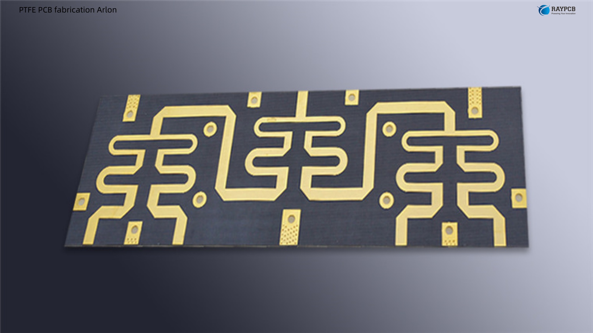
Complete guide to PTFE PCB fabrication using Arlon AD Series laminates. Covers drilling parameters, sodium naphthalene vs plasma etch surface preparation, PTFE/FR4 hybrid lamination, plating adhesion, controlled impedance testing, common defects, and practical process guidance for RF PCB manufacturers.
The first time a PCB fabricator runs PTFE material without proper preparation, the results are memorable — and not in a good way. Smeared via walls that won’t plate. Delaminated layers at the PTFE/epoxy interface. Copper peeling from a surface that looked fine until it didn’t. PTFE is a chemically inert, mechanically soft polymer that behaves fundamentally differently from the glass-epoxy system your operators have spent years perfecting. Standard FR4 process parameters applied to PTFE produce scrap, not boards.
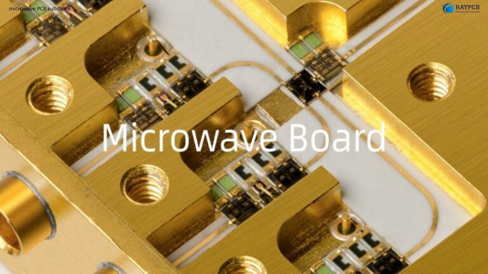
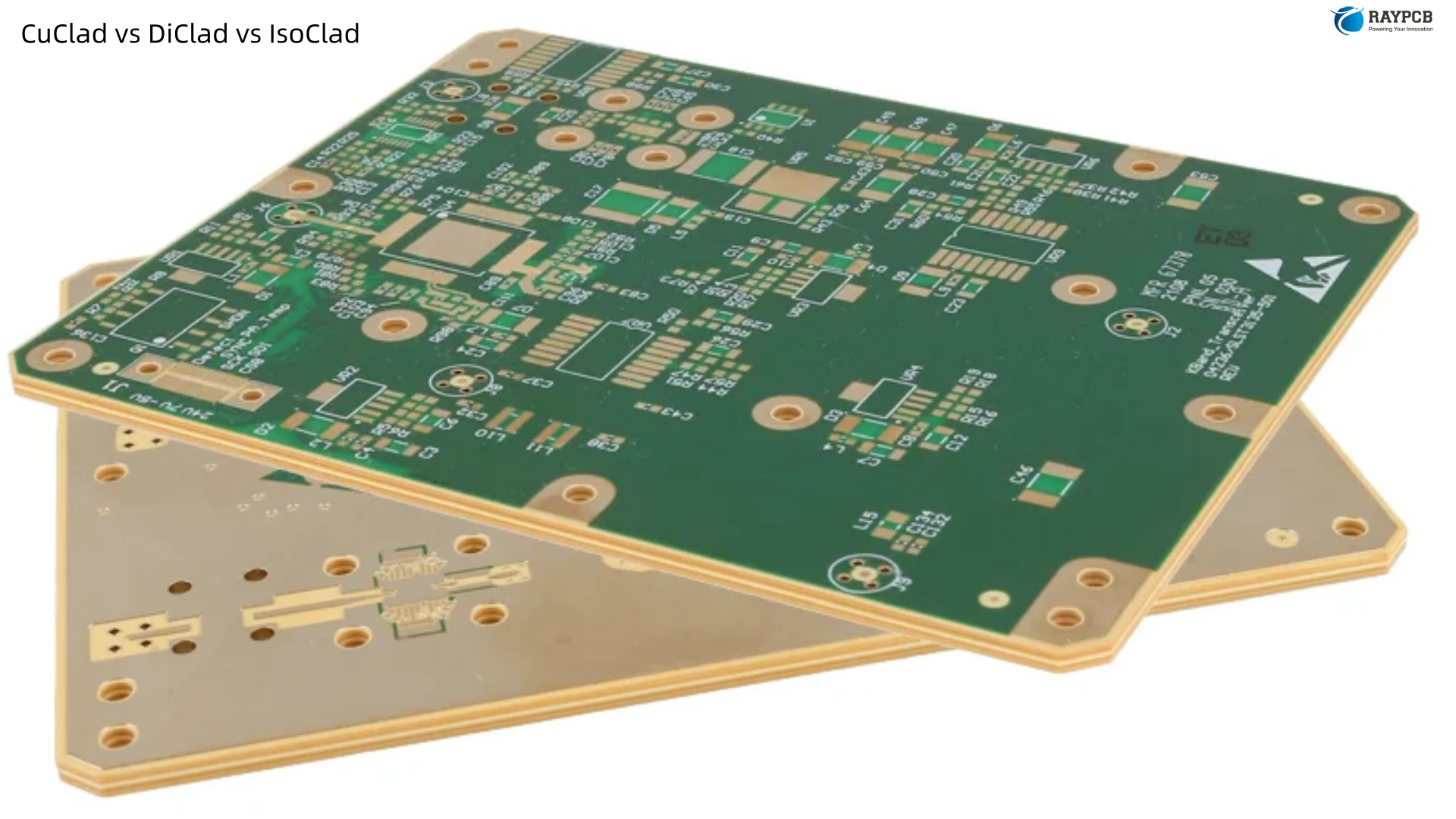
PTFE PCB fabrication with Arlon AD Series laminates is a discipline of its own. The AD Series — including AD250C, AD300D, AD350A, and related variants — is Arlon’s family of woven PTFE composite materials targeting RF, microwave, and millimeter-wave applications from antenna substrates to defense electronics to automotive radar. These materials deliver exceptional electrical performance (Dk from 2.50 to 3.50, Df in the 0.0015–0.0025 range), but extracting that performance in a finished, reliable multilayer board requires understanding and respecting PTFE’s material chemistry at every step of the fabrication sequence.
This guide is written for process engineers and PCB designers who are either setting up PTFE capability for the first time or troubleshooting an existing PTFE process on Arlon AD Series materials. We’ll cover the full fabrication sequence from incoming material handling through final inspection, with specific attention to the steps where PTFE diverges most sharply from FR4 practice.
Understanding the Arlon AD Series Laminate Family
Before getting into process, it’s worth being clear about what the AD Series actually is, because the product line covers meaningful variations in Dk, filler loading, and construction that affect process parameters.
The AD designation refers to Arlon’s antenna-grade dielectric composite family. All AD Series materials share a woven PTFE matrix, but differ in ceramic filler loading, which tunes the Dk:
| Material | Dk @ 10 GHz | Df @ 10 GHz | Construction | Primary Application |
| AD250C | 2.50 ± 0.04 | 0.0015 | Woven PTFE / ceramic | Low-Dk antenna structures, SIW |
| AD300D | 3.00 ± 0.04 | 0.0020 | Woven PTFE / ceramic | Wideband antenna feeds, satcom |
| AD350A | 3.50 ± 0.05 | 0.0025 | Woven PTFE / ceramic | Patch arrays, filter circuits |
| AD450 | 4.50 ± 0.05 | 0.0030 | PTFE / ceramic composite | High-Dk antenna miniaturization |
For fabrication purposes, the key shared characteristic is that all AD Series materials are PTFE-based, which means every process step that is FR4-specific — drill parameters, desmear chemistry, surface preparation — must be replaced with PTFE-appropriate alternatives. The ceramic filler loading affects material hardness somewhat, which influences drill wear rates, but the fundamental process requirements are the same across the AD Series family.
For engineers working on Arlon PCB designs, understanding these material family distinctions before engaging a fabricator prevents the most common qualification problems.
Step 1: Incoming Material Handling and Storage for Arlon AD Series
PTFE laminates require more controlled storage than FR4. Unlike glass-epoxy, PTFE does not absorb moisture significantly (AD Series moisture absorption is typically <0.04%), but the material is susceptible to:
- Surface contamination from handling oils that compromise copper adhesion during lamination
- Mechanical damage from improper stacking — PTFE panels are softer than FR4 and can be gouged by panel edges or tooling pins
- Dimensional instability if stored in environments with significant temperature cycling before lamination
Recommended Storage Conditions
Store Arlon AD Series panels flat in the original packaging in a clean, temperature-controlled environment (15–25°C, 40–60% RH). Do not stack unpacked panels directly — use interleaving paper or foam separators. Handle panels with clean cotton or nitrile gloves; bare hand contact deposits skin oils on the copper surface that can cause adhesion failures in subsequent plating steps.
Before cutting panels to working size, inspect incoming material for lamination voids, copper surface defects, and dimensional conformance to the purchase specification. Arlon ships material with a Certificate of Conformance (C of C) — verify that the Dk, copper weight, and thickness match your design specification before releasing to production.
Step 2: Panel Preparation and Shear Cutting
PTFE composites can be shear-cut on standard laminate cutters, but the soft PTFE matrix requires sharper blades and slower cutting speeds than FR4. Dull blades compress rather than cut PTFE fibers, leaving a ragged edge that can delaminate during subsequent processing.
Key parameters for shear cutting AD Series panels:
- Use sharp blades — inspect and replace more frequently than FR4 practice
- Reduce cutting speed by 20–30% compared to FR4
- Support the panel fully to prevent flexing during the cut
- Chamfer any sharp panel corners that will contact the drill fixture to reduce edge chipping
After cutting, mark panel orientation relative to the warp/fill direction of the woven PTFE fabric. Dk is slightly anisotropic in woven PTFE materials — the dielectric constant in the warp direction can differ from the fill direction by 0.02–0.05 depending on the specific AD variant. For antenna designs with tight Dk tolerance requirements, consistent panel orientation relative to the antenna axis is good practice.
Step 3: Drilling PTFE PCBs — The Most Critical Process Step
Drilling is where PTFE fabrication diverges most significantly from FR4, and where the most common PTFE fabrication failures originate. Getting drilling right is the foundation of everything that follows — a poorly drilled hole cannot be fixed in desmear or plating.
Why Standard FR4 Drill Parameters Fail on PTFE
PTFE is a viscoelastic polymer with a Young’s modulus roughly 30x lower than cured FR4. It deforms elastically under the drill bit rather than fracturing cleanly. At FR4 drill speeds (typically 60,000–100,000 RPM for small vias), PTFE generates frictional heat faster than it dissipates, softening locally and smearing against the via wall rather than being removed as chips. The result is a via wall coated with re-solidified PTFE smear that blocks copper plating adhesion — identical in principle to the resin smear problem in FR4, but caused by a different mechanism and requiring completely different chemistry to remove.
Recommended Drill Parameters for Arlon AD Series
The following parameters are starting points for Arlon AD Series materials. Every drill machine, bit geometry, and stack configuration requires empirical validation — these are guidelines, not universal settings.
| Parameter | FR4 Typical | Arlon AD Series PTFE | Notes |
| Spindle Speed | 80,000–120,000 RPM | 40,000–60,000 RPM | Lower speed reduces frictional heating |
| Feed Rate (infeed) | 60–100 in/min | 80–130 in/min | Higher feed rate removes heat via chip extraction |
| Retract Rate | 400–600 in/min | 300–500 in/min | Reduce to minimize PTFE stretching on retract |
| Hit Count per Bit | 2,000–3,000 | 500–800 | PTFE accelerates bit wear — replace more frequently |
| Stack Height | 3–4 panels | 1–2 panels | Reduce stack to maintain chip extraction |
| Entry Material | Aluminum | Aluminum | Same — provides surface support |
| Backup Material | Phenolic | Phenolic or FR4 | Prevents PTFE panel lifting |
| Coolant | None (dry) | None or CO₂ cooling | CO₂ improves via quality in fine pitch |
The counterintuitive combination of lower spindle speed and higher feed rate is the core insight for PTFE drilling. Higher feed rate per revolution increases the chip load, which means more material is removed per rotation and heat has less time to build up at the cutting edge. Operators accustomed to FR4 will instinctively want to slow the feed rate when drilling feels different — resist this instinct on PTFE.
Drill Bit Selection for PTFE
Use solid carbide drills with geometry optimized for non-ferrous, soft materials — some suppliers offer PTFE-specific drill geometries with modified helix angles. Standard FR4 drill bits function on PTFE but wear faster and produce lower-quality via walls. For production programs on Arlon AD Series, invest in PTFE-optimized tooling and track bit life aggressively with microsection inspection at regular intervals.
Step 4: Surface Preparation — Replacing Permanganate with PTFE-Compatible Chemistry
This is the step where the most engineers new to PTFE PCB fabrication with Arlon materials run into an absolute wall. Standard potassium permanganate desmear chemistry, which is the universal FR4 via preparation process, does not work on PTFE. Permanganate attacks and oxidizes the epoxy resin in FR4, creating a micro-roughened surface that copper plating adheres to. PTFE is chemically inert to permanganate — the chemistry has no effect on the via wall, which means you get no surface activation, which means your copper plating has nothing to bond to.
Two process approaches work on PTFE:
Sodium Naphthalene (Tetraetch) Treatment
Sodium naphthalene etch — commonly sold under the trade name Tetraetch — is the traditional surface preparation chemistry for PTFE. It works by chemically defluorinating the PTFE surface, creating dangling carbon bonds that can form adhesive bonds with subsequent copper plating. The treated surface turns visibly brown/dark, which is normal and indicates successful defluorination.
Process considerations for sodium naphthalene:
- Sodium naphthalene solution is hazardous — requires proper handling, storage, and waste disposal infrastructure
- Treatment time must be controlled precisely — under-treatment leaves inadequately activated surface, over-treatment degrades PTFE mechanically
- The treatment is anisotropic — it activates the PTFE surface but does not significantly affect the ceramic filler particles in AD Series composites
- Parts must be rinsed thoroughly after treatment to remove all residual chemistry before plating
Plasma Etch Surface Preparation
Plasma etch using oxygen, nitrogen/hydrogen, or CF4/O2 gas mixtures is an increasingly preferred alternative to sodium naphthalene for PTFE surface activation. Plasma etch creates reactive surface species that promote copper adhesion, is more controllable than wet chemistry, and eliminates the hazardous chemical handling associated with sodium naphthalene.
For Arlon AD Series materials, oxygen plasma etch in the 100–300 W range with controlled exposure time provides effective surface activation. Plasma etch is the preferred process for fabs with existing plasma equipment from FR4 desmear or semiconductor-grade PCB processes.
| Preparation Method | Effectiveness | Infrastructure Required | Hazard Level | Preferred For |
| Sodium naphthalene (Tetraetch) | Excellent | Wet chemistry line | High | High-volume PTFE lines |
| Oxygen plasma etch | Very Good | Plasma chamber | Low | Lower volume, newer facilities |
| CF4/O2 plasma | Excellent | Plasma chamber | Medium | Fine-geometry PTFE |
| Potassium permanganate | None | Standard FR4 line | Low | FR4 only — does NOT work on PTFE |
Step 5: Electroless Copper Deposition
After surface preparation, Arlon AD Series panels proceed through standard electroless copper (PTH — plated through hole) deposition. The electroless copper process itself does not require modification for PTFE, provided the surface preparation step has been executed correctly. If sodium naphthalene or plasma etch has properly activated the PTFE surface, standard palladium catalyst and electroless copper chemistries will produce adequate adhesion.
However, PTFE’s lower surface energy compared to FR4 means the catalyst adsorption step may be less robust. Extending the palladium catalyst dwell time by 20–30% compared to FR4 practice improves plating uniformity, particularly on the PTFE-rich regions of the via wall in AD Series composites. Run microsection samples at this stage to verify copper coverage uniformity before proceeding to electrolytic plating.
Step 6: Lamination of Arlon AD Series Multilayer Boards
Multilayer lamination of PTFE boards involves several process considerations that differ from standard FR4 lamination. The fundamental challenge is that PTFE does not flow and bond under heat and pressure the way epoxy prepregs do — a standard FR4 prepreg cannot be used to bond PTFE layers together or to bond a PTFE layer to an adjacent FR4 layer.
PTFE-to-PTFE Bonding
For bonding two AD Series PTFE layers together in a multilayer stack, Arlon provides dedicated bondply materials — specifically the AD7068 series of PTFE-based bondplies — that are formulated to wet and adhere to PTFE surfaces under appropriate heat and pressure cycles. These bondplies are thin PTFE composite sheets pre-coated with an adhesive system compatible with the PTFE matrix.
Lamination parameters for PTFE-to-PTFE bonding with Arlon bondply:
| Parameter | Typical Range | Notes |
| Press Temperature | 180–200°C | Lower than FR4 cure temperature |
| Press Pressure | 200–400 psi | Verify with Arlon process guide |
| Cure Time | 60–120 minutes | Depends on stack thickness |
| Cooling Rate | Slow (controlled) | Rapid quench can cause warpage |
| Vacuum | Required | Prevents voids at bondline |
PTFE-to-FR4 Hybrid Lamination
When building hybrid stack-ups with Arlon AD Series PTFE layers adjacent to standard FR4 layers — the most common configuration in commercial radar and telecommunications hardware — the bonding chemistry at the interface requires particular attention. Standard FR4 prepregs do not bond reliably to PTFE surfaces. The interface requires either:
- A PTFE-compatible adhesive layer (such as Arlon’s AD7068 bondply) between the PTFE and FR4 sections, or
- A specialized hybrid prepreg that is compatible with both the PTFE and FR4 chemistries
Thermal expansion mismatch between PTFE (high Z-CTE) and FR4 (moderate Z-CTE) creates stress at the interface during thermal cycling. For AD Series materials with moderate Z-CTE performance, this mismatch is manageable in most commercial temperature ranges (-40°C to +85°C), but should be validated with thermal cycling coupons before production commitment.
Dimensional Stability During Lamination
Woven PTFE composites have lower in-plane dimensional stability during lamination compared to FR4. Panel artwork registration needs to account for this by using larger tolerance bands on via-to-copper annular ring minimums, or by using a dedicated pin lamination system with PTFE-qualified tooling. Request your fab’s measured dimensional variation data on Arlon AD Series builds before designing tight via-to-copper features.
Step 7: Imaging, Etching, and Surface Finish
After lamination and plating, the standard PCB imaging and etching sequence applies to Arlon AD Series boards with minimal modification. The copper foil on PTFE laminates etches with the same chemistry (ammoniacal, cupric chloride, or ferric chloride) as FR4 copper. Line width and spacing are controlled by photolithography and etch parameters as on FR4, though:
- At 77 GHz or similar frequencies, trace width tolerances are tight — request 1-sigma line width data from your fab for the specific etch process
- PTFE’s lower surface energy can affect dry film photoresist adhesion in fine-line imaging — validate photoresist compatibility with the specific Arlon AD Series surface before committing to fine-pitch designs
For surface finish on Arlon AD Series RF boards, ENIG (Electroless Nickel Immersion Gold) is the standard choice, as it provides a flat, solderable surface compatible with SMT assembly and wire bonding of MMICs. HASL (Hot Air Solder Leveling) is generally avoided on fine-pitch RF designs because the uneven surface height variation affects transmission line impedance at millimeter-wave frequencies.
Step 8: Post-Fabrication Inspection and Testing
PTFE PCB boards require the same post-fabrication inspection steps as FR4 but with additional attention to PTFE-specific failure modes:
Microsection Analysis
Microsection inspection is more critical on PTFE builds than FR4. Specifically verify:
- Via wall copper coverage uniformity — particularly at PTFE-rich zones versus ceramic-filler zones
- PTFE smear absence — via walls should show clean copper without PTFE film intrusion
- Bondline integrity at PTFE/FR4 or PTFE/PTFE interfaces in hybrid builds
- Annular ring dimensions conforming to IPC-6012 Class requirements
Controlled Impedance Testing
At the frequencies Arlon AD Series materials are used for, impedance testing is non-negotiable. Every production panel should include impedance test coupons measured by TDR (Time Domain Reflectometry) or VNA (Vector Network Analyzer) to verify that the fabricated stack-up achieves the target impedance within specification. Dk variation within the ±0.04–0.05 tolerance band directly affects impedance, and production measurement closes the loop between the design simulation and the actual board.
Insertion Loss Verification
For programs where insertion loss is a specified deliverable, fabricate representative test coupons with through-line and thru-reflect-line (TRL) calibration structures on each panel. Measure insertion loss with a VNA calibrated to the coupon launch geometry. Compare measured loss to simulation to verify that the material’s Dk and Df match the datasheet values used in your design model.
Common PTFE Fabrication Defects and Root Causes
| Defect | Likely Root Cause | Corrective Action |
| Poor copper adhesion to via wall | Inadequate PTFE surface activation | Verify sodium naphthalene / plasma etch process |
| PTFE smear in via | Drill speed too high / feed rate too low | Reduce RPM, increase feed rate |
| Delamination at PTFE/FR4 interface | Incompatible bondply or incorrect press profile | Use Arlon AD7068 bondply; verify press temperature |
| Via wall voids | Insufficient catalyst dwell time in PTH line | Extend palladium catalyst immersion time |
| Panel warpage after lamination | Rapid cooling or asymmetric stack-up | Use controlled cooling cycle; balance copper distribution |
| Copper peel on PTFE surface | Surface contamination before lamination | Enforce clean handling protocols; inspect with contact angle |
| Impedance out of spec | Dk variation in material or etch tolerance | Verify material lot Dk; tighten etch process control |
Useful Resources for PTFE PCB Fabrication with Arlon AD Series
| Resource | Description | Link |
| Arlon AD Series Datasheets | Full electrical, mechanical, and thermal specs for all AD variants | arlon-mmc.com |
| Arlon Process Guide for PTFE Laminates | Fabrication recommendations for drilling, desmear, and lamination | arlon-mmc.com |
| IPC-4103 | Qualification and performance spec for high-frequency laminates | ipc.org |
| IPC-6012 Class 3 | PCB performance and qualification — high-reliability applications | ipc.org |
| IPC-TM-650 | Test methods referenced throughout fabrication and inspection | ipc.org |
| IPC-7711/7721 | Rework and repair for high-reliability PCBs | ipc.org |
| Polar Si9000e | Controlled impedance field solver for RF PCB stack-up design | polarinstruments.com |
| Ansys HFSS | 3D EM simulation for via transitions and antenna structures | ansys.com |
| RayPCB Arlon PCB Guide | Overview of Arlon material families and fabrication context | raypcb.com/arlon-pcb |
Frequently Asked Questions: PTFE PCB Fabrication with Arlon AD Series
Q1: Can a standard FR4 PCB fabricator run Arlon AD Series PTFE boards without new equipment?
In most cases, no — not without meaningful process investment. The minimum requirements are: a dedicated PTFE drilling line with appropriate speed/feed control, sodium naphthalene or plasma etch capability for surface preparation (which requires either a dedicated wet chemistry line or a plasma chamber), and validated lamination press profiles for PTFE-compatible bondply materials. Fabs that already run other PTFE-based materials (Rogers RT/duroid, Taconic TLX, etc.) will adapt to Arlon AD Series with relatively minor process validation work. A pure FR4 shop attempting PTFE for the first time should expect a meaningful qualification effort — plan for 2–4 validation builds before committing production.
Q2: How do I choose between sodium naphthalene etch and plasma etch for Arlon AD Series surface preparation?
Both methods effectively activate the PTFE surface for copper plating adhesion. The practical choice is usually driven by your existing infrastructure. Sodium naphthalene is effective and well-established but requires hazardous chemical handling, dedicated wet chemistry infrastructure, and careful disposal. Plasma etch is cleaner, more controllable, and preferred in new PTFE process setups — but requires capital investment in plasma chamber equipment if you don’t already have it. For high-volume production with an existing sodium naphthalene line, there’s little reason to change. For a new PTFE process qualification, plasma etch is the recommended direction.
Q3: What is the shelf life of Arlon AD Series PTFE laminates, and does storage affect electrical properties?
PTFE-based laminates generally have excellent shelf life compared to B-stage epoxy prepregs. Arlon AD Series panels stored under the recommended conditions (clean, temperature-controlled, in original packaging) typically remain usable for 12–24 months. Unlike FR4 prepreg, the PTFE matrix does not continue curing or age during storage. Moisture absorption (<0.04%) is negligible, so humidity excursions within normal storage ranges don’t significantly affect electrical properties. The primary aging concern is copper surface oxidation, which can affect plating adhesion — this is why original packaging should be maintained until the material is ready for use, and why incoming inspection of copper surface condition is important.
Q4: How does via aspect ratio affect PTFE PCB fabrication on Arlon AD Series, and what are the practical limits?
Via aspect ratio (board thickness divided by drill diameter) significantly affects fabrication yield in PTFE more than FR4, because the PTFE drilling process is more sensitive to chip extraction conditions, and because PTFE’s surface activation chemistry must reach and adequately treat the full via wall depth. Practical via aspect ratios for reliable production on Arlon AD Series are generally limited to 8:1 or less for through-hole vias — more conservative than the 10:1 sometimes achieved on FR4 under optimized conditions. For high-aspect-ratio vias (>6:1), increase drill bit replacement frequency, validate via wall quality by microsection at multiple depths through the build qualification, and consider specifying blind/buried via structures where layout allows to reduce required aspect ratios.
Q5: Can Arlon AD Series boards be reworked after assembly if component soldering defects occur?
PTFE boards are more susceptible to localized thermal damage during rework than FR4, primarily because PTFE’s low thermal conductivity means heat from a rework iron concentrates locally rather than spreading across the laminate. The practical risks are: copper pad lifting if excessive dwell time or temperature is applied, PTFE softening and deformation under direct heat, and flux residue penetration into the laminate surface if the board is not properly cleaned. Rework is possible with appropriate precautions — use the lowest effective tip temperature, shortest possible dwell time, and non-activated (ROL0) flux. For production programs on Arlon AD Series, design-for-rework principles (adequate pad geometry, appropriate component clearances) and operator training on PTFE rework sensitivity will protect yield significantly better than attempting to repair poorly designed reworkability after the fact.
Final Thoughts on PTFE PCB Fabrication with Arlon AD Series
Successful PTFE PCB fabrication with Arlon AD Series materials is achievable and routine at fabs that have invested in the process knowledge and chemistry infrastructure. The process is not exotic or mysterious — it’s a discipline with well-understood parameters that requires respecting PTFE’s fundamentally different material chemistry at each step.
The engineers and process teams who consistently get first-pass success on Arlon AD Series builds share a common approach: they treat the PTFE process as a distinct discipline from FR4 rather than a variation on it. They validate drill parameters empirically on test panels before production runs. They don’t allow shortcuts on surface preparation chemistry. They use the right bondply at PTFE/FR4 interfaces. And they inspect with microsection at regular intervals to catch process drift before it generates a full panel of scrap.
The electrical performance available in Arlon’s AD Series — Dk from 2.50, Df in the 0.0015–0.0025 range, excellent temperature stability — justifies every bit of the additional process investment for the applications that demand it.
Meta Description Suggestion:
Long version (editorial use):
Complete guide to PTFE PCB fabrication using Arlon AD Series laminates. Covers drilling parameters, sodium naphthalene vs plasma etch surface preparation, PTFE/FR4 hybrid lamination, plating adhesion, controlled impedance testing, common defects, and practical process guidance for RF PCB manufacturers.
Trimmed version for Google (158 characters — within Yoast green zone):
PTFE PCB fabrication guide for Arlon AD Series: drilling parameters, surface preparation, hybrid lamination, plating adhesion, defect troubleshooting, and inspection tips.