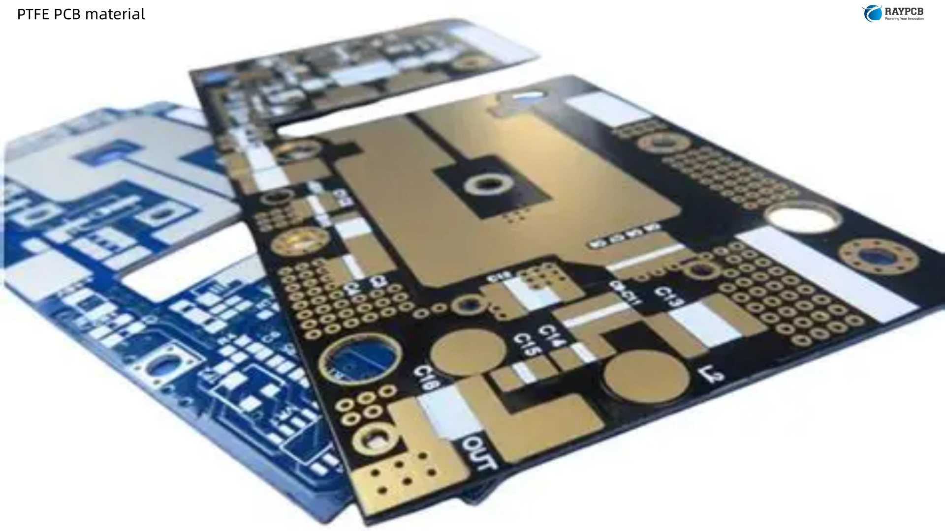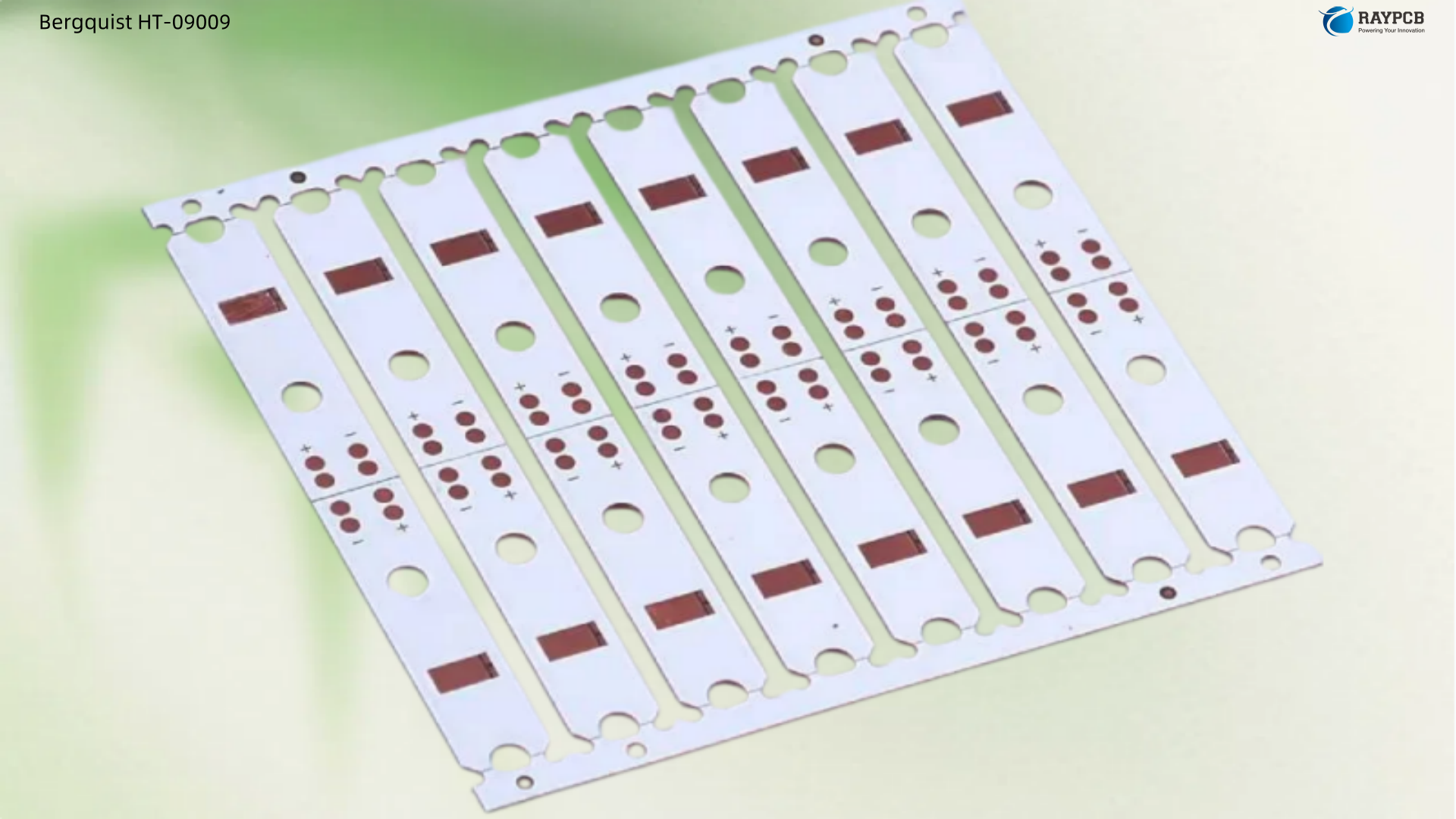
Technical guide to the Bergquist HT-09009 high temperature MCPCB dielectric — specs, thickness comparison, applications in high-voltage power electronics, and fabrication tips.
If you’re specifying dielectric materials for a metal core PCB that has to survive high operating temperatures, handle lead-free solder reflow without flinching, and hold its electrical isolation properties across thousands of thermal cycles — you’ve probably already encountered the Bergquist HT series. The Bergquist HT-09009 occupies a specific and important place in that lineup: it’s the thicker-dielectric option in the High Temperature (HT) family, engineered for applications where greater electrical isolation headroom, higher breakdown voltage, and multi-layer assembly compatibility are non-negotiable.
This article gives you a detailed technical picture of what the HT-09009 actually is, how it fits within the broader Thermal Clad product family, what makes it the right choice for certain demanding applications — and where you’d choose a different grade instead.
What Is Bergquist Thermal Clad and Why the Dielectric Is Everything
Bergquist is a US-based company that invented thermal clad PCBs. Henkel acquired Bergquist on September 1, 2014 and now offers technological solutions for electronics using Bergquist thermal management products.
Thermal Clad Insulated Metal Substrate (IMS) was developed by Bergquist as a thermal management solution for today’s higher watt-density surface mount applications where heat issues are a major concern. Thermal Clad substrates minimize thermal impedance and conduct heat more effectively and efficiently than standard printed wiring boards.
What makes Bergquist’s approach distinctive compared to competitors who just use standard prepreg is the dielectric formulation. The dielectric is a proprietary polymer/ceramic blend that gives Thermal Clad its excellent electrical isolation properties. Different from others, Bergquist doesn’t use fiberglass, allowing for better thermal performance. Glass carriers degrade thermal performance, which is why their dielectrics are glass-free.
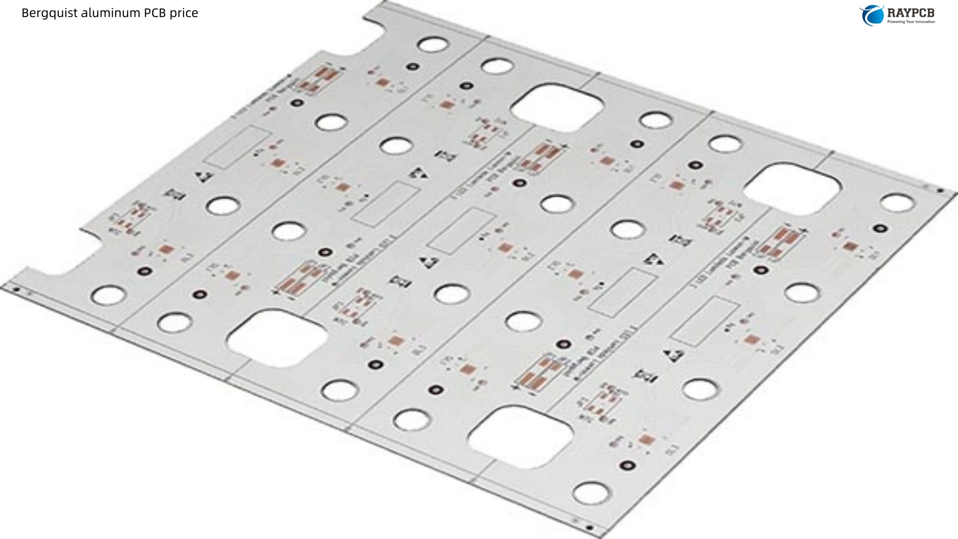
Thermal Clad is a three-layer system comprised of a circuit layer (printed circuit foil with a thickness of 1 oz. to 10 oz.), a dielectric layer that offers electrical isolation with minimum thermal resistance, and a base layer that is often aluminum but other metals such as copper may also be used.
Understanding this architecture is essential before diving into the HT-09009 specifically, because the entire engineering case for MCPCB design hinges on what that dielectric layer can and can’t do.
Understanding the Bergquist HT Series Product Naming Convention
How to Read the HT Part Number
Bergquist’s Thermal Clad product codes follow a systematic naming structure that encodes key performance parameters directly into the part number. For the HT series:
- HT = High Temperature dielectric family
- The digits that follow encode thermal conductivity (in tenths of W/m·K) and dielectric thickness (in mils)
Using this convention, the HT-09009 decodes as follows:
| Code Element | Meaning | HT-09009 Value |
| HT | Dielectric family | High Temperature |
| 090 | Thermal conductivity indicator | ~2.2 W/m·K nominal |
| 09 | Dielectric thickness | 9 mil (229 µm) |
For comparison, here’s how other HT series products decode:
| Part Number | Dielectric Thickness | Thermal Conductivity | Thermal Impedance |
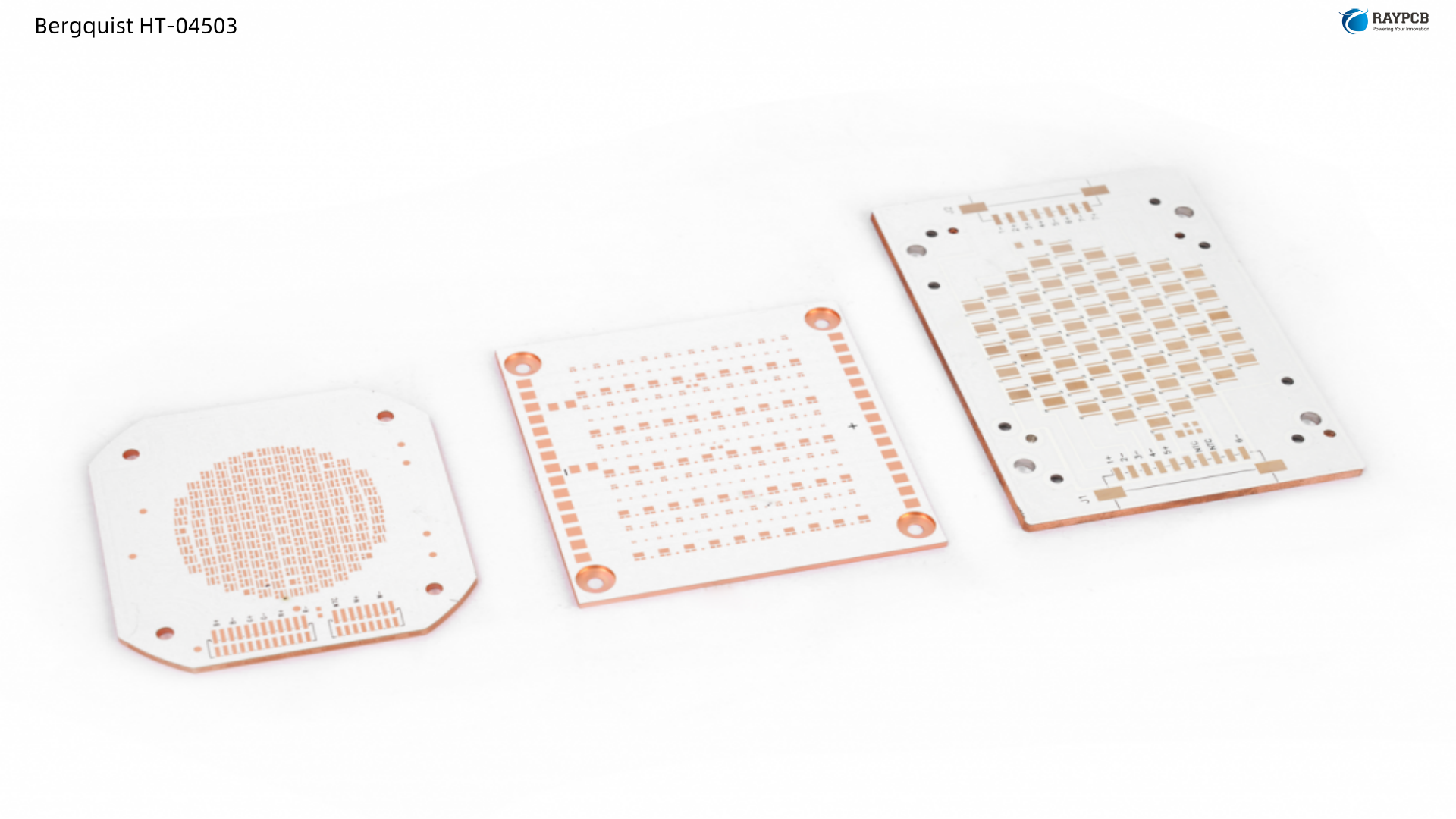
| HT-04503 | 3 mil (76 µm) | 4.1 W/m·K | 0.05°C·in²/W |
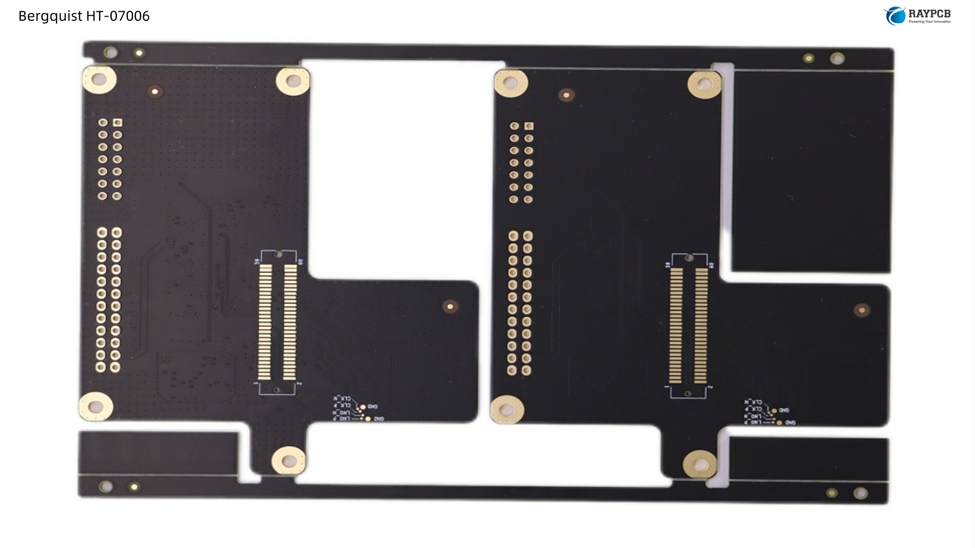
| HT-07006 | 6 mil (152 µm) | 2.2 W/m·K | 0.27°C·in²/W |
| HT-09009 | 9 mil (229 µm) | ~2.2 W/m·K | Higher (thicker dielectric) |
The thicker the dielectric, the higher the thermal impedance but also the higher the dielectric breakdown voltage. The HT-09009 exists specifically for situations where that trade-off makes sense — when you need more breakdown voltage headroom than the 6-mil or 3-mil options provide.
Bergquist HT-09009 Key Technical Specifications
The HT-09009 shares the core material chemistry of the entire HT dielectric family, with the distinguishing factor being its 9-mil (229 µm) dielectric thickness. Based on Bergquist’s published HT series data, the following properties apply:
Thermal Properties
| Property | Value | Test Method |
| Thermal Conductivity | ~2.2 W/m·K | ASTM D5470 |
| Thermal Impedance (typical) | Higher than HT-07006 | ASTM D5470 |
| Max Operating Temperature (UL) | 130°C continuous | UL 746B |
| Max Soldering Temperature | 288°C (10 seconds) | IPC TM-650 2.4.13 |
| UL Solder Rated | 325°C / 60 seconds | UL recognition |
| Glass Transition Temperature (Tg) | >130°C (higher thermal grades) | ASTM E1356 |
Electrical Properties
| Property | Value | Test Method |
| Dielectric Thickness | 9 mil (229 µm) | — |
| Dielectric Breakdown (typical) | >15 kVAC | ASTM D149 |
| Dielectric Strength | ~2,000 V/mil | ASTM D149 |
| Dielectric Constant (εr) | ~4.2 at 1 MHz | ASTM D150 |
| Dissipation Factor | ~0.02 at 1 MHz | ASTM D150 |
| Volume Resistivity | >10⁹ MΩ·cm | ASTM D257 |
| Surface Resistivity | >10⁹ MΩ/sq | ASTM D257 |
Mechanical and Chemical Properties
| Property | Value |
| Peel Strength | ≥5 lb/in (0.9 N/mm) |
| Flammability | UL 94V-0 |
| RoHS Compliance | Yes |
| Halogen-Free | Yes |
| Water Absorption (168 hrs) | <0.20% |
| CTE (x/y-axis) | ~18–20 ppm/°C |
Important Note: Always verify current specifications against the official Henkel/TCLAD technical data sheet for your application. Dielectric performance can vary with copper weight and base metal selection.
What Makes the HT-09009 Specifically Suited for High Voltage and Multi-Layer Applications
Higher Dielectric Breakdown Voltage
For applications with an expected voltage over 480 Volts AC, Bergquist recommends a dielectric thickness greater than 0.003″ (76 µm). The HT-09009’s 9-mil (229 µm) thickness provides roughly three times the dielectric thickness of that minimum threshold, giving it substantial breakdown voltage headroom for high-voltage motor drives, inverters, and industrial power conversion equipment operating at or above 480V AC.
In power electronics, every volt of margin you can build into electrical isolation is real reliability you can count on in the field. The thicker dielectric in the HT-09009 translates directly into safer clearances in applications where transient overvoltage events, lightning strikes, or inductive switching spikes are expected.
Multi-Layer MCPCB Stack-Up Compatibility
Bergquist Thermal Clad substrates are not limited to use with metal base layers. Power conversion applications can enhance their performance by replacing FR-4 with Thermal Clad dielectrics in multi-layer assemblies. In this application, the thickness of the copper circuit layer can be minimized by the high thermal performance of Thermal Clad.
The HT-09009’s thicker dielectric makes it particularly well-suited to this multi-layer role. When Thermal Clad dielectric is used as the bonding/insulation layer between circuit layers in a hybrid multilayer assembly, the 9-mil variant provides better inter-layer isolation than the 3-mil or 6-mil options — at the cost of slightly higher thermal impedance. For multilayer assemblies where control circuits and high-voltage power circuits coexist in the same stack-up, that isolation is often mandatory.
Eutectic Gold/Tin and Lead-Free Solder Compatibility
HT dielectrics are UL solder rated at 325°C/60 seconds, enabling Eutectic Gold/Tin solders. This is not a capability that standard MCPCB materials can match. For applications in aerospace, military electronics, or high-reliability optoelectronics where AuSn eutectic die attach is required, the HT series dielectrics — including the HT-09009 — are among the few commercially qualified options that can withstand the process temperatures involved.
HT-09009 vs. Other Bergquist HT Dielectrics: Choosing the Right Thickness
This is the question that matters most in practice. The HT series is not a one-size-fits-all product family. Here’s how the options map to application requirements:
| Dielectric Grade | Thickness | Thermal Impedance | Breakdown Voltage | Best Application |
| HT-04503 | 3 mil (76 µm) | 0.05°C·in²/W | ~6 kVAC | Maximum thermal performance, lower voltage (<480V) |
| HT-07006 | 6 mil (152 µm) | 0.27°C·in²/W | ~11 kVAC | General high-temperature power electronics |
| HT-09009 | 9 mil (229 µm) | Higher | ~15+ kVAC | High voltage, multi-layer, AuSn die attach |
Choose HT-09009 when:
- Your bus voltage exceeds 480V AC and you need conservative breakdown margins
- You’re designing a multilayer MCPCB assembly where inter-layer isolation is critical
- Your assembly process uses Eutectic AuSn solder and requires >300°C process compatibility
- You need the best moisture and contamination resistance across the HT product range (thicker dielectric)
Choose HT-07006 or HT-04503 when:
- Thermal impedance is your primary design constraint and voltage is below 480V
- You’re building single-layer LED or power supply boards where maximum heat transfer takes priority
- Cost is a factor — thinner dielectrics are less expensive per panel
Bergquist HT-09009 vs. Competing High Temperature MCPCB Dielectrics
The Bergquist/TCLAD HT series isn’t the only game in town for high-temperature MCPCB applications. Here’s how HT-09009-class materials compare to alternatives:
| Material | Supplier | Thermal Conductivity | Dielectric Thickness | Max Solder Temp | Distinctive Feature |
| HT-09009 | Bergquist/TCLAD | ~2.2 W/m·K | 9 mil (229 µm) | 325°C/60s | AuSn compatible, multi-layer |
| HT-07006 | Bergquist/TCLAD | 2.2 W/m·K | 6 mil (152 µm) | 325°C/60s | Standard HT, LED/power |
| HT-04503 | Bergquist/TCLAD | 4.1 W/m·K | 3 mil (76 µm) | 325°C/60s | Highest thermal conductivity in HT series |
| Arlon 92ML | Arlon PCB | 2.0+ W/m·K | Various | High | Military-grade reliability |
| Ventec VT-4B1 | Ventec | 2.0 W/m·K | 4 mil | 288°C | Cost-competitive HT alternative |
| Laird Tflex | Laird | 1.0–6.0 W/m·K | Phase-change | — | Thermal interface material, not laminate |
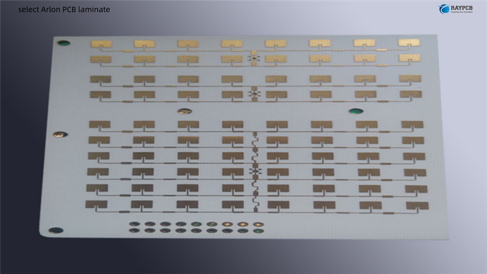
A Note on Arlon
It’s worth calling out Arlon PCB materials as a legitimate alternative for high-temperature MCPCB dielectric applications, particularly for designs headed into military or aerospace environments. Arlon brings deep heritage in demanding reliability applications, and their high-temperature dielectric laminates are often evaluated alongside Bergquist HT grades in mil-spec qualification programs. The choice between them typically comes down to fabricator qualification, supply chain considerations, and whether a specific military or aerospace program already has one manufacturer qualified.
Primary Applications for the Bergquist HT-09009
Motor Drives and Variable Frequency Drives (VFDs)
Compact high-reliability motor drives built on Thermal Clad have set the benchmark for watt-density. Dielectric choices provide the electrical isolation necessary to meet operating parameters and safety agency test requirements. The availability of Thermal Clad HT makes high temperature operation possible.
The HT-09009 in particular is favored for VFDs operating on 480V AC industrial power systems. The combination of thicker dielectric, high Tg, and lead-free solder compatibility makes it well-matched to the thermal and electrical stress profile of IGBT-based motor control circuits.
High-Voltage Power Conversion
Due to the size constraints and watt-density requirements in DC-DC conversion, Thermal Clad has become the favored choice. It is available in a variety of thermal performances, is compatible with mechanical fasteners and is highly reliable. It can be used in almost every form-factor and fabricated in a wide variety of substrate metals, thicknesses and copper foil weights.
For AC-DC power supplies and DC-DC converters operating at or above 48V bus with primary-to-secondary isolation requirements, the HT-09009 provides the kind of working voltage headroom that gives safety certification agencies confidence and gives design engineers sleep at night.
Solid State Relays (SSRs) and Switches
High-voltage solid state relays are among the most classic applications for HT-grade MCPCB materials. The combination of high current density, high bus voltage, and compact form factor in SSRs makes the elevated breakdown voltage and high-temperature solderability of HT-09009 particularly valuable.
Multi-Layer Hybrid Assemblies
A multi-layer MCPCB has multiple layers of circuitry, a metal core, and a dielectric material. The multiple layers of circuitry are sandwiched between the insulation layers. These PCBs are compact-sized and used in applications where space is limited and require efficient heat dissipation. Multi-layer thermal clad PCBs are used in various applications including satellite systems, atomic accelerators, heart monitors, and file servers.
In these multi-layer configurations, the HT-09009’s 9-mil dielectric provides meaningful inter-layer electrical isolation — essential when high-voltage power routing shares a stack-up with sensitive control or signal layers.
Design and Fabrication Considerations for HT-09009 MCPCB
Base Metal Selection
Available base metals include 5052 Aluminum in thicknesses of 0.8 mm to 3.2 mm, 6061 Aluminum from 0.8 mm to 4.8 mm, 4045 Aluminum, and Copper C1100 in various thicknesses. Most common thicknesses are 1.0 mm and 1.5 mm for aluminum bases.
For high-voltage applications using HT-09009, 1.5 mm or 2.0 mm aluminum base is the most common choice — thick enough for good heat spreading while remaining manageable for routing and mechanical mounting.
Copper Foil Weight
Copper foil weight options include ED Copper in 1 oz (35 µm), 2 oz (70 µm), 3 oz (105 µm), 4 oz (140 µm), and 6 oz (210 µm), and RA Copper in 8 oz (280 µm) and 10 oz (350 µm).
For power applications with the HT-09009, 2 oz or 3 oz copper is typical. Heavier copper improves current-carrying capability and spreads heat more effectively in the circuit layer — but increasing copper thickness while maintaining circuit flatness requires maintaining the copper layer at roughly 10% of the aluminum base thickness or thinner.
Lead-Free Assembly and Soldering
The HT-04503 and HT series dielectrics are lead-free solder compatible and Eutectic AuSn compatible, RoHS compliant and environmentally green, and available on all aluminum and copper metal substrates. These properties extend across the HT family, including the HT-09009.
Dielectric Integrity Testing
Any micro-fractures, delaminations or micro-voids in the dielectric will breakdown or respond as a short. Due to the capacitive nature of the circuit board construction, it is necessary to control the ramp up of the voltage to avoid nuisance tripping of the failure detect circuits in the tester and to maintain effective control of the test.
This is a practical point that catches out engineers new to MCPCB testing. The hi-pot test procedure for MCPCB dielectrics requires a slow voltage ramp — typically 100–500 V/s — rather than the abrupt application used for standard PCB isolation testing.
Useful Resources for Bergquist HT-09009 and MCPCB Design
Official Product Documentation
- Henkel/TCLAD HT Dielectric Technical Data Sheet — Current published specs for the HT series including thermal impedance and electrical properties
- Bergquist Thermal Clad Selection Guide (Digikey) — Full engineering guide covering all dielectric families, base metal selection, circuit layer options, and assembly recommendations
- TCLAD Product Page — Current Henkel/TCLAD product catalog and contact information for sampling
Standards and References
- IPC-4101: Specification for Base Materials for Rigid and Multilayer Printed Boards — Laminate qualification standard framework
- ASTM D5470: Standard Test Method for Thermal Transmission Properties of Thermally Conductive Electrical Insulation Materials — The thermal conductivity test method cited in Bergquist datasheets
- UL 94 Flammability Standard — Bergquist HT materials carry UL 94V-0 recognition
Design Tools
- Bergquist Thermal Impedance Charts — Pages 8–9 of the Selection Guide contain thermal impedance curves for all dielectric families as a function of copper foil thickness
- Digi-Key Bergquist MCPCB Products — Search “Bergquist Thermal Substrates” for stocked MCPCB panels
5 Frequently Asked Questions About the Bergquist HT-09009
Q1: What is the main difference between the HT-09009 and HT-07006, and when should I choose the thicker grade?
Both are high temperature dielectrics from the same product family with the same base polymer/ceramic chemistry. The HT-09009’s 9-mil dielectric offers roughly 35% more thickness than the HT-07006’s 6-mil, which translates to higher dielectric breakdown voltage and greater inter-layer isolation for multi-layer assemblies — at the cost of higher thermal impedance. Choose the HT-09009 when your bus voltage exceeds 480V AC, when you’re building a multi-layer MCPCB where isolation between power and control layers is critical, or when your process uses Eutectic AuSn solder die attach that demands maximum process temperature robustness. Choose HT-07006 when thermal performance is the primary constraint and your voltage is within moderate bounds.
Q2: Is the Bergquist HT-09009 compatible with standard FR4 fabrication processes?
Partially. The HT-09009 uses the same photo-chemical etching processes as standard FR4 for circuit layer patterning. However, because the base is aluminum or copper rather than glass-epoxy, drilling requires different tooling and parameters — you’re typically routing rather than drilling through the full metal base for board outline, and via formation works differently in MCPCB designs. Solder mask and surface finish processes are compatible with standard SMT equipment. Fabricators experienced in MCPCB production will handle HT-09009 without issue; a fabricator who only runs FR4 will need to qualify the process before committing to production quantities.
Q3: What base metal should I choose for an HT-09009 application at 480V industrial voltage?
For 480V AC industrial applications, 6061 aluminum at 1.5 mm or 2.0 mm thickness is the most common choice. It provides the mechanical rigidity for rack-mounted power conversion equipment, good thermal spreading, and is compatible with standard machine screws for chassis mounting. If your thermal budget is very tight or your current density is extreme, copper base is an option — but it costs significantly more and is heavier. Copper base is generally reserved for applications where thermal performance is so demanding that aluminum simply can’t provide adequate heat spreading, such as very high-density IGBT modules.
Q4: How does the HT-09009 perform through repeated thermal cycling compared to standard MCPCB dielectrics?
The HT dielectric family was specifically formulated for high-temperature durability. The polymer/ceramic blend maintains its mechanical and electrical properties across wide temperature ranges and through repeated thermal cycling from −40°C to +125°C and beyond in many applications. The critical variable is the coefficient of thermal expansion (CTE) match between the dielectric, the copper foil, and the aluminum base. CTE mismatch generates cyclic stress that can eventually delaminate the dielectric from the base metal or crack solder joints. Bergquist’s HT formulation is engineered to minimize this mismatch, but for extreme cycling profiles — automotive under-hood, for instance — run accelerated thermal cycle testing on your specific build before committing to production.
Q5: Where can I order Bergquist HT-09009 material, and what are typical lead times?
The HT-09009 is a standard Bergquist/TCLAD product available through authorized distributors including Digi-Key, Mouser, and Arrow Electronics for prototype and low-volume quantities. For production volumes, direct purchase through Henkel/TCLAD sales channels or authorized converter fabricators is typical. Lead times for standard configurations (aluminum base, 1 oz or 2 oz copper, standard thicknesses) are typically 2–4 weeks from stock distributors, though custom base metal alloys, unusual foil weights, or non-standard panel sizes may require 4–8 weeks. Always check current stock status with your distributor, as specific thickness/copper weight combinations may be made-to-order.
Final Thoughts: Is the Bergquist HT-09009 Right for Your MCPCB Design?
The HT-09009 is not the default choice for every MCPCB application. It’s a specialized grade within the Bergquist HT family, optimized for the specific engineering situation where you need both high-temperature dielectric performance and elevated breakdown voltage — typically in industrial high-voltage power conversion, motor drives above 480V, multi-layer hybrid assemblies, or applications requiring Eutectic AuSn die-attach compatibility.
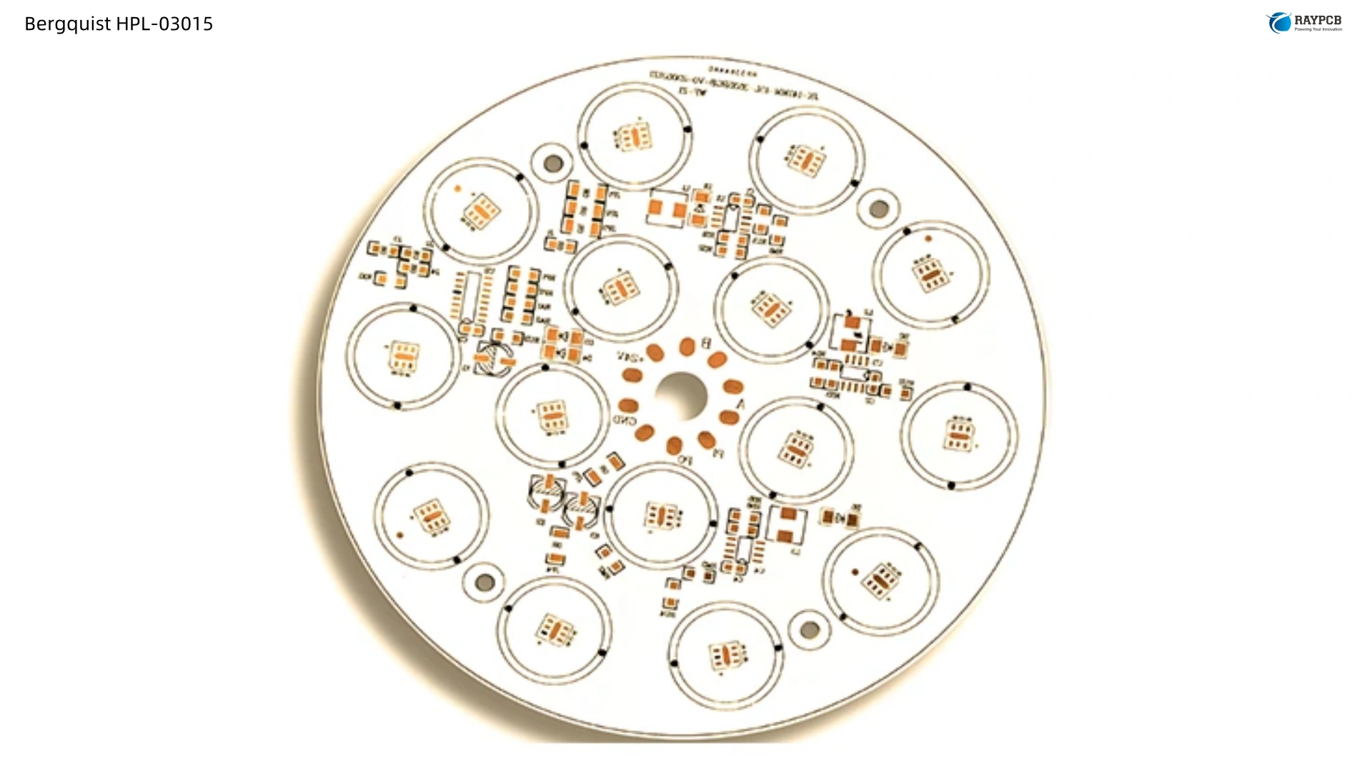
If your application runs below 480V and thermal impedance is your primary concern, the HT-04503 delivers dramatically better thermal performance with its 3-mil dielectric. If you’re specifying LED lighting or general-purpose power supply boards, the HT-07006 or the HPL family may be better fits.
But when the voltage is high, the temperatures are punishing, and the reliability stakes are real — the HT-09009 is the Bergquist dielectric that was designed for exactly that design challenge.
For MCPCB fabrication using Bergquist HT-09009 and other specialty Thermal Clad materials, work with a fabricator who has a qualified process for IMS/MCPCB production, including dielectric hi-pot testing and certified lead-free assembly capability.