
RAYPCB · RF materials & manufacturing
RT/duroid 5880LZ PCB manufacturing
Specify low-density PTFE core thickness, handling and finished RF geometry. Review the material data, use the engineering model, and send a defined construction for quotation.
Bring your band, stackup, quantity and acceptance requirements. Preliminary files are welcome for review.
Material data and construction choices
Low-density PTFE is a separate grade
5880LZ has a different dielectric and material construction from RT/duroid 5880. Do not use one page title as proof of interchangeability. The low-density construction deserves its own handling, mechanical support and RF model review. Confirm the ordered thickness and foil before comparing line dimensions or planning a bonded assembly.
| Property | Supplier reference | Engineering meaning |
|---|---|---|
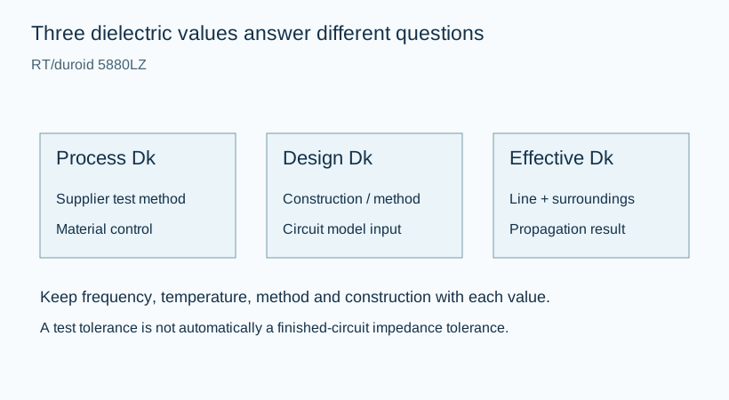
| Process Dk | 2.00 +/- 0.04 | Supplier process reference; use the original method and construction. |
| Design Dk | 2.0 | Separate modeling reference. Confirm applicability to the chosen geometry. |
| Typical Df | 0.0021 | Property-tool heading: 10 GHz; parenthetical values refer to 2.5 GHz. Check grade notes. |
| Typical thermal conductivity | 0.33 W/m·K | Consult the grade source for direction and method; not a finished-board power rating. |
| Typical X / Y / Z CTE | 54 / 47 / 40 ppm/K | The source table states its temperature interval. Axis and conditions matter. |
| Material flammability reference | V-0 | Supplier material listing, not certification of a fabricated board or assembly. |
Source: RT/duroid 5880LZ manufacturer product data and the Rogers laminate property tool. Values are material references; purchasing and finished-board acceptance need their own agreed specification.
RF engineering workbench
Use explicit construction inputs. Results can be downloaded or opened as an email draft; the tool does not upload project information.
Worked planning example
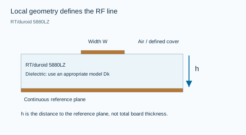
As a calculation example, use the published RT/duroid 5880LZ design reference Dk of 2, a 0.508 mm dielectric height and a 50 Ω target. The zero-thickness microstrip model gives approximately 1.665 mm trace width and effective permittivity 1.741. At 10 GHz, its guided wavelength is approximately 22.719 mm. The selected height and frequency are example inputs, not an assertion that this is an available or approved material construction.
Use the result to inspect scale and sensitivity. Preserve the input units and assumptions in the downloaded brief, then use the actual finished geometry and appropriate solver or measurement method for release.
RAYPCB ENGINEERING
Rogers EngineeringRogers Engineering Workbench
Loading Rogers Engineering Workbench…
Glass-microfiber PTFE: low-Dk circuits with construction discipline
A glass-microfiber PTFE laminate uses a different reinforcement arrangement from woven-glass PTFE. Low dielectric constant can support RF structures with relatively wide lines for a given dielectric height and impedance. The same property generally produces longer guided wavelengths than a higher-Dk material. Whether that is useful depends on the antenna, feed, filter or transmission-line task. Physical size, routing space and mechanical support should be considered with the electrical loss target.
Specify the exact RT/duroid grade. Similar numbers do not establish equivalence: 5870, 5880 and 5880LZ have separate property sets and construction considerations. A statement such as low-loss PTFE leaves the fabricator without a complete material purchase description. Add dielectric thickness, its tolerance, copper type and weight, and any approved alternate. If a dimensional requirement was derived from an inch-based standard construction, preserve that identity instead of silently rounding it to a different metric thickness.
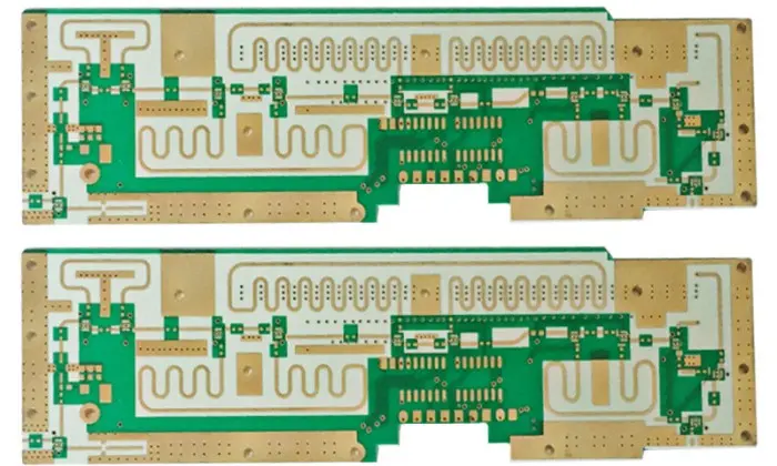
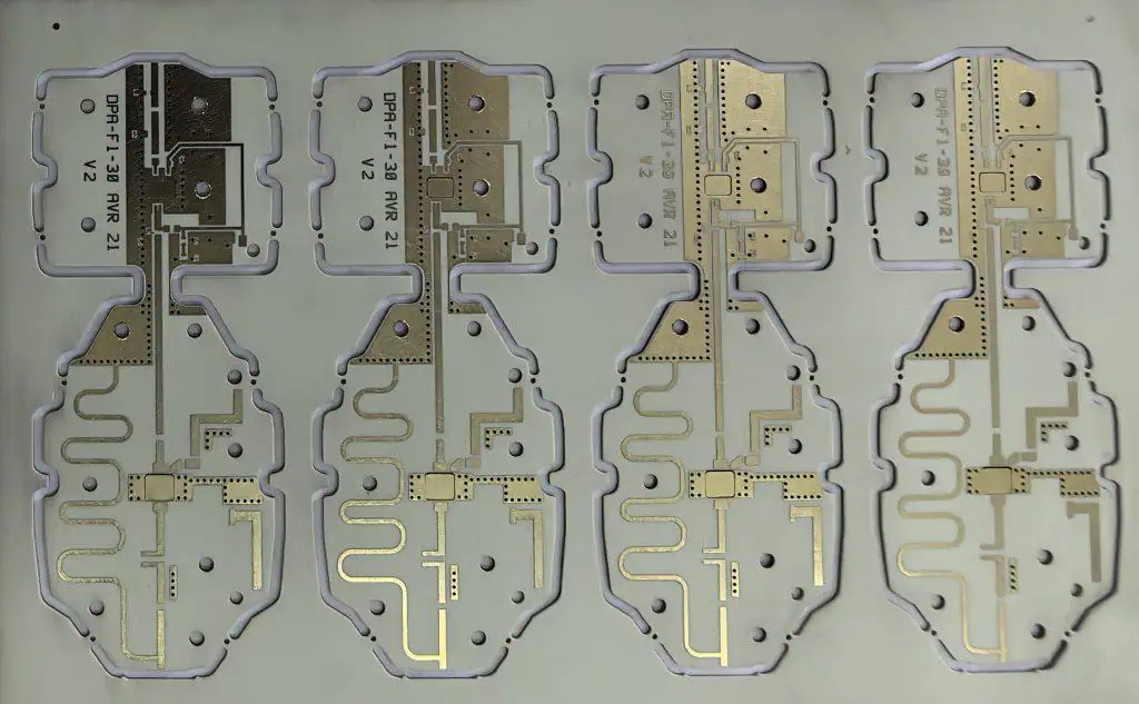
A thin RF core may need support during processing and in the final assembly. The support could be a carrier, a bonded metal base or another part of the multilayer. Those elements change the mechanical and thermal environment, and some can influence the RF geometry. Draw them explicitly. An image of a two-sided circuit does not establish whether a particular customer's board needs a backing plate, adhesive or special attachment method.
The nearly isotropic dielectric behavior discussed for some microfiber materials is an electrical property under stated conditions. It does not mean every mechanical property, thermal expansion direction or fabrication response is isotropic. Keep electrical and mechanical assumptions separate. When measuring a phase-sensitive circuit, preserve the actual structure, fixture and environmental conditions; do not use a broad material description as a substitute for a test plan.
After etching, dimensional response depends on the material and copper pattern. This is a manufacturing planning issue because locations established before stress redistribution may no longer represent the same final positions. Follow the relevant supplier guidance and the fabricator's qualified procedure. Avoid copying a generic bake temperature into the drawing without checking the complete construction, since adhesives, finishes and previous process steps may impose different constraints.
Define the board that should be quoted and manufactured
An RF board quotation is most useful when it describes the same construction that the design team intends to release. State the exact laminate grade, dielectric thickness, copper and finished board thickness separately. Add the layer sequence, outline and drill information. For a multilayer, name the bonding products rather than listing only the outer RF core. If a choice is still open, identify it as an engineering question in the request.
Mark the RF dimensions that deserve particular attention. Examples include a narrow coupling gap, a connector launch, a resonator edge or a line routed over a specific reference plane. A controlled-impedance requirement should identify the signal layer, reference layer, target and tolerance. It should also state the coupon or measurement expectations when those are part of acceptance. A generic statement that all traces are fifty ohms is rarely enough to resolve a complex circuit.
Keep finished copper and base foil distinct. Plating and etching can change the conductor cross-section used in the electrical model. Surface finish, solder mask and nearby cover materials can also affect exposed RF structures. Ask the fabrication review to return any proposed change to these assumptions before the design is frozen. An unexplained substitution can make an apparently cheaper quotation difficult to compare with the intended build.
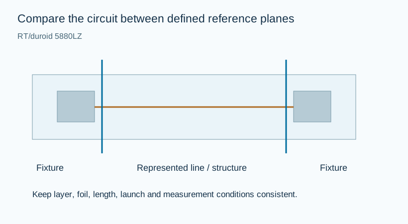
The first build should test the assumptions that matter to the product. A continuity result verifies connectivity. An impedance coupon provides evidence for its represented line structure. RF insertion-loss, phase or filter-response testing requires additional fixtures, reference planes and acceptance conditions. Agree the scope before ordering so that the delivered records answer the intended engineering question.
For assembly, add the bill of materials, placement data, assembly drawing and test plan. Include special connector, heat-spreader or device-attachment requirements early. The fabrication and assembly scopes can then be reviewed together while remaining separately identifiable in the quotation. The direct enquiry route on this page is available without completing the calculators; the tools simply help make the technical brief clearer.
Cost planning and a direct RFQ route
Where the cost changes, and which savings are real
For a small RF order, setup, procurement and test preparation may matter as much as the area of laminate. A panel that holds more circuits spreads some shared effort across more boards, but only if the orientation, tooling and coupon requirements permit that layout. The budget tool uses an explicit rectangular nesting model so that its area assumption can be inspected. It does not assume every visible square millimeter of a panel becomes a delivered board.
Copper foil, core thickness and bonding system are part of the purchased construction. A quotation based on a different thickness or foil is not a clean price comparison, even when the headline material name matches. Ask whether the offered material is standard for the supplier's available construction and whether minimum purchases, special handling or qualification work affect the lot. Availability and lead time must be confirmed for the actual order rather than inferred from a web page.
Complexity can move cost in several directions. A hybrid stack may reduce the amount of premium RF laminate while adding press planning and interface review. Metal backing can improve a thermal path while adding bonding and machining requirements. Extra coupons or RF fixtures can reduce uncertainty but add material, setup and measurement work. Compare the complete project scope instead of ranking designs by laminate price alone.
The optional numerical budget uses cost allowances entered by the visitor. It contains no calibrated RAYPCB tariff and does not claim current market pricing. The model combines the costed panels, one-time setup, batch testing and per-board processing; assembly is included only when selected and entered. Shipping, taxes, process yield loss and unentered qualification are excluded. A zero value means already included or deliberately zero, not unknown.
When geometry, quantity or supply scope changes, revisit the allowances. A per-board processing cost from one batch may not apply to another. The tool clears old allowances on those changes to avoid presenting a stale total. Hybrid, metal-backed, unresolved and more complex multilayer constructions go to engineering quotation. The downloaded brief remains useful because it carries the requirements and assumptions even when a numerical price would be misleading.
RAYPCB ENGINEERING
Rogers EngineeringRogers Fabrication Budget & RFQ
Loading Rogers Fabrication Budget & RFQ…
Prefer to send files now? Contact the RAYPCB team with the requested material, construction and quantity. An exact quotation is based on the agreed scope.
Verify the construction that matters to the product
A measurement plan that answers the design question
Begin with what the prototype must establish. Is the question electrical continuity, line impedance, insertion loss, phase balance, resonant frequency, thermal behavior or mechanical fit? These are different tests and they may require different coupons, fixtures and acceptance limits. A test label without the represented structure and measurement method leaves room for two parties to interpret the result differently.
For RF measurements, define the reference planes and account for the launch or fixture. A raw network-analyzer trace can include connectors and transitions that are not part of the material comparison. De-embedding or a representative reference structure may be needed, depending on the question. Record calibration, frequency span, temperature and the circuit revision with the result. This makes later comparisons more informative than a single unqualified pass statement.
Investigate a disagreement between the model and the board in a controlled sequence. Check the finished conductor dimensions, dielectric height, material construction and measurement setup before changing the Dk to force a fit. The model may omit a nearby cover, a return-path discontinuity or a loss mechanism. Equally, the test fixture may represent a different structure from the intended coupon. Identifying the cause protects the next build from an accidental compensation.
Keep the accepted construction and records together. A successful prototype supports the tested revision under its stated conditions. Changes to material, foil, bond system, geometry, assembly exposure or test scope deserve review before a repeat order is treated as equivalent. The project does not need every possible test; it needs the evidence that resolves its actual risks and acceptance requirements.
RAYPCB ENGINEERING
Rogers EngineeringRogers Construction Explorer
Loading Rogers Construction Explorer…
Questions before the next design or purchase decision
What should this page help me decide?
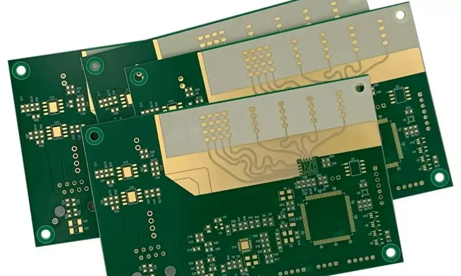
Specify low-density PTFE core thickness, handling and finished RF geometry. Start with the named construction and the relevant engineering requirement. The photographs show physical circuit examples, while the original-source links and explicit model assumptions support the technical review.
Which Dk should I enter for RT/duroid 5880LZ?
The supplier process reference is 2.00 +/- 0.04; the separate design reference is 2.0. Use the value and method appropriate to the actual construction and model. Effective permittivity is a line-geometry result, not a replacement label for either material value.
What is the most important construction detail here?
Exact 5880LZ construction. Keep that decision in the released drawing and ask the supplier to identify the offered construction explicitly. For this material, the follow-up verification should address low-density core support and rf geometry.
Does the design tool approve this PCB for manufacture?
No. It calculates the stated preliminary model or organizes a construction brief. Finished copper, transitions, mixed dielectrics, assembly interfaces and process limits may require a more complete review. The downloaded result preserves assumptions so engineering can evaluate the same inputs.
Can I obtain a price without completing the tool?
Yes. Use the direct Contact or email route with your drawing, quantity and construction requirements. The optional budget uses your entered allowances and an explicit panel model; it is not a calibrated RAYPCB tariff. Complex constructions need a file-based quotation.
What should I send with an enquiry?
Include the exact material designation, fabrication artwork, drill data, outline, proposed stackup, copper, finish and quantity. Add the relevant impedance, RF, thermal or mechanical acceptance requirements. If assembly is included, provide the BOM, placement data and test expectations.
Continue with the right engineering task
Original technical references
Supplier documents support material identity, properties and methods. They do not establish current stock or qualify an unspecified finished board. Check the exact grade, construction and document revision for your order.