
Wangling · Material guide
F4BME Low-PIM PCB Material
Translate a foil-related PIM choice into a board test requirement.
Wangling distinguishes F4BME by its reverse-treated copper-foil option within the F4BM/F4BME family. This is a material-selection input; the assembled RF path has additional possible nonlinear contacts.
Send preliminary files or a released drawing. Identify the material, quantity and open decisions.
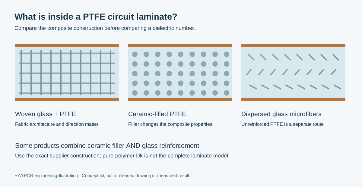
Decision first. Define the test tones, power levels, connectors and acceptance reference for PIM. Do not quote a material headline as the measured PIM of a finished RAYPCB circuit.
01 / Material evidence
What to know about F4BME Low-PIM PCB Material
| Review item | What to use |
|---|---|
| Material / subject | F4BME Low-PIM PCB Material |
| Primary decision | Translate a foil-related PIM choice into a board test requirement |
| Construction control | Exact grade, revision, dielectric thickness and foil |
| Design data | Use the approved supplier sheet and geometry model |
| Application task | Antenna feeds with PIM requirements |
| Useful next step | Send the drawing and material requirement |
Family and application descriptions are selection guidance. Availability, production limits, pricing and acceptance scope require a project review.
Reference: Wangling — original material construction information.
02 / Your engineering task
Specify the PIM test as a circuit requirement
Passive intermodulation can arise at nonlinear interfaces in the RF path. Material and foil choices are relevant, but connectors, finishes, soldered contacts and mechanical joints also belong in the assessment. A laminate result cannot establish the behavior of every finished assembly using it.
Define the tone frequencies, power, termination, fixtures and reporting reference. Keep the test arrangement consistent when comparing material options. If the acceptance requirement is expressed relative to carrier power, make sure both the reference and measurement bandwidth are documented.
Treat a change in foil, connector attachment or contact finish as a review item even if the dielectric core remains unchanged. An effective manufacturing enquiry asks for the precise construction and test scope. It does not ask a supplier to guarantee a general low-PIM label without measurable conditions.
| Continue when you need… | Next page |
|---|---|
| Specify the construction and copper rather than a broad family | F4BM-1/2 PTFE PCB Material |
| Use the exact AD250C electrical values and foil option | AD250C PCB Laminate |
| Choose a documented F4B family construction | F4B-1/2 PTFE Laminate |
03 / Engineering calculations
RF design workbench: width, phase and loss
Work with F4BME Low-PIM PCB Material using the exact construction data. Select a line model or a planar passive calculation. Results explain the assumptions and can be downloaded with the entered values.
RAYPCB ENGINEERING
PTFE EngineeringPTFE RF Design Workbench
Loading PTFE RF Design Workbench…
Read dielectric data in the right context
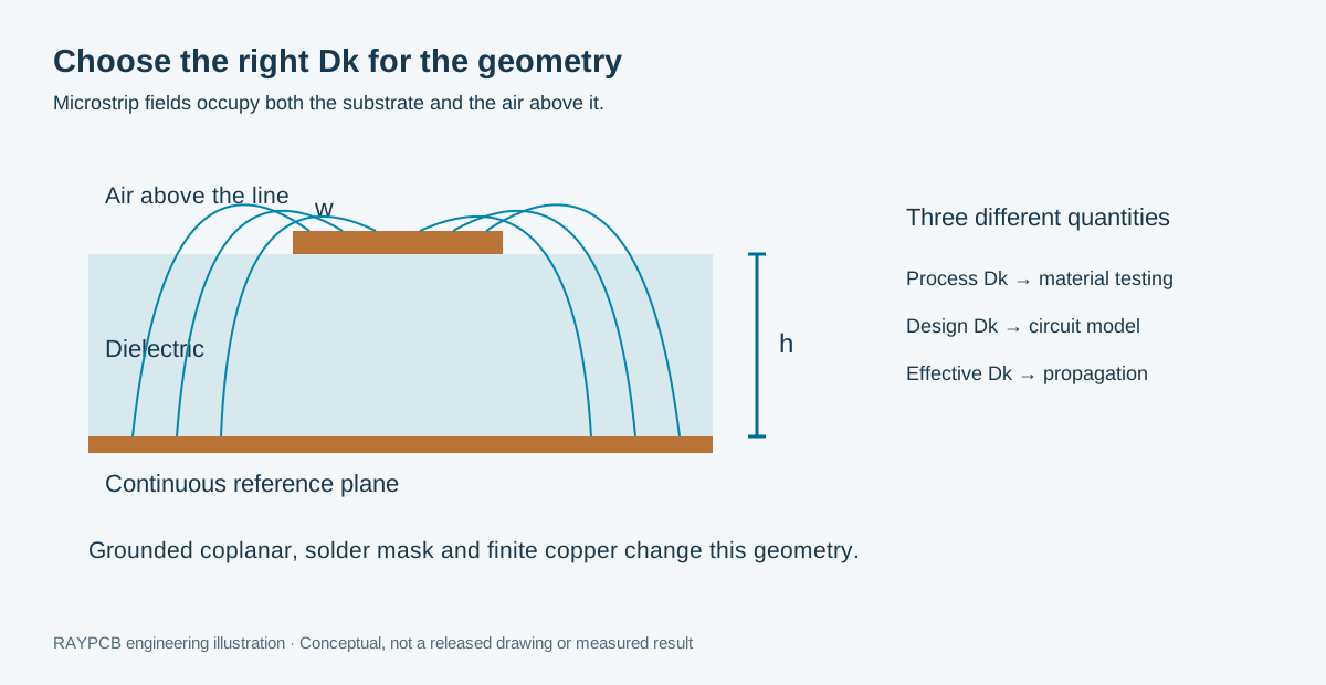
A material data table and a circuit simulation answer different questions. Process Dk is used in a defined material measurement. Design Dk is a supplier modeling reference. Effective permittivity belongs to the transmission-line geometry and includes how its fields occupy the surrounding media. Keep those labels attached when copying values into a drawing, a calculator or an RF model. An unlabeled number is difficult to audit later.
For a microstrip, identify the distance between the trace and its continuous reference plane. Do not enter total board thickness unless that dimension really is the dielectric height. For centered stripline, this workbench asks for total ground-plane spacing. An asymmetric stripline, a coplanar line with backside ground, solder mask over the trace or a mixed-dielectric stack requires a model that actually represents those features.
Use the calculation to establish scale and sensitivity. The workbench uses a zero-thickness, quasi-static line model, so it does not compensate for finished copper, etch shape, roughness, dispersion or transitions. A narrower nominal trace is not automatically a better layout. Check routability and tolerances, then correlate the chosen geometry with a field solver and an agreed fabrication coupon.
04 / Scope and budget
Cost planning and a usable quotation brief
Use this form when preparing a F4BME Low-PIM PCB Material enquiry. You can also go straight to Contact without calculating. The budget is optional and uses your own board-specific cost allowances.
RAYPCB ENGINEERING
PTFE EngineeringPTFE Fabrication & Budget Brief
Loading PTFE Fabrication & Budget Brief…
Compare cost using the same construction and acceptance scope
The laminate price is only one part of a finished RF board quotation. Ordered sheet format, panel utilization, copper, layer count, holes, bonding, handling and inspection all affect the manufacturing plan. Small quantities can carry a larger share of setup and test-fixture effort. An apparent material saving may disappear if it requires a new layout, additional coupons or a repeat qualification build.
For a meaningful comparison, hold the board outline, quantity, acceptance criteria and deliverable constant. Ask which material grade, thickness, foil and bond system each proposal assumes. Separate bare-board fabrication from component purchasing and assembly. Also separate continuity testing from impedance or RF measurements so that a lower price is not simply a smaller test scope.
The quotation tool generates a project brief by default. Optional budget numbers use your entered allowances, not a RAYPCB tariff or current market price. Its scenario range is not a statistical confidence interval. Complex hybrids, metal-backed structures, unresolved grades and special qualification work go to engineering quotation. Freight, tax and any work not explicitly entered remain outside the calculation.
05 / Review the construction
Design-to-build review for F4BME Low-PIM PCB Material
Allocate the complete RF loss and phase budget
Begin with the ports and the allowed electrical behavior between them. State the operating band, reference impedance, loss limit and any phase-matching requirement. Include transmission lines, vias, connectors, soldered interfaces, filters and other structures that are inside the measurement reference planes. Without that definition, two apparently different board results may simply include different parts of the signal path.
Dielectric-only attenuation is one contribution to insertion loss. Copper conductivity, conductor profile, surface roughness, finish, radiation and mismatch can also matter. A loss-tangent value measured at one frequency is not a measured loss curve over a whole band. The tool deliberately identifies its constant-Df assumption and excludes these other contributions; it should not be used to promise finished-board performance.
For phase-sensitive paths, preserve the material model, geometry and temperature assumptions together. Equal drawn lengths can still have different electrical lengths when their reference structures differ. A layer change, a ground interruption or a different connector launch deserves review. Define whether the acceptance requirement concerns absolute delay, phase at one frequency or tracking over a band and temperature range.
Design details to settle before routing is frozen
Define a continuous return path for every RF region. Avoid treating a ground label on the schematic as proof that the physical reference is uninterrupted. Plane slots, cutouts, antipads and changes in reference layer alter the fields. When a signal changes layers, review the accompanying return connection and launch geometry rather than considering only the signal via diameter.
Keep the finished conductor definition explicit. Base foil thickness and plated thickness are different. Etch compensation belongs in the fabrication review, while the designer needs to know which width the impedance model describes. If mask, cover material or a metal enclosure is close enough to influence the fields, include that environment in the final model and drawing.
Use coupons that represent the important construction and routing conditions. Their layer, foil, reference plane and measurement method should be agreed before panelization. Leave space for fixtures or connectors if RF measurements are required. A generic coupon on a convenient spare layer may not answer the engineering question posed by the actual signal path.
06 / Evidence and release
Prepare the next engineering review
Approve the first build and control the next revision
Agree the first-build acceptance plan before the order enters fabrication. Useful records can include material identity, stackup confirmation, dimensional checks, connectivity results, impedance measurements and application-specific RF evidence. The actual list depends on the project. Do not assume that a laminate datasheet, a supplier certificate or a photograph substitutes for finished-board inspection.
When a coupon result differs from the model, compare the same reference structure and test method before changing the material value. Check finished geometry, dielectric height, foil assumptions, fixture influence and calibration. Record any agreed compensation with the drawing revision so that a repeat order does not inadvertently revert to the original nominal dimensions.
Keep an approved build record containing material designation, laminate revision, stackup, circuit revision, permitted substitutions and test limits. Review changes to foil, bond material, panel orientation, assembly exposure or supplier route before treating the next lot as identical. A successful prototype demonstrates that particular build under its test conditions; it does not eliminate the need for controlled production changes.
RAYPCB ENGINEERING
PTFE EngineeringPTFE Stackup Explorer
Loading PTFE Stackup Explorer…
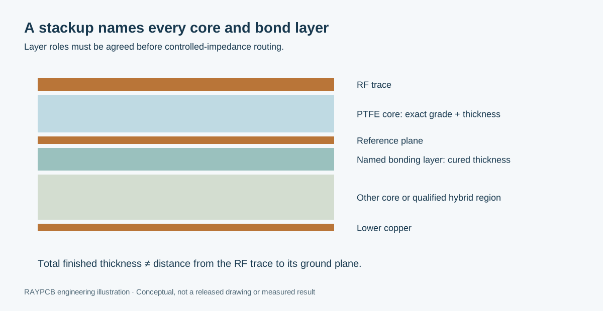
The layer sequence is a conceptual explanation. It does not assign an adhesive to this material or approve a press cycle. For detailed construction planning, use RF Multilayer PCB Design with PTFE.
What to send for an engineering quotation
Send the circuit artwork in the agreed fabrication format, drill data, board outline, mechanical notes, quantity and revision. Add a stackup that names every core and bonding layer, dielectric thickness, copper requirement and surface finish. Identify open decisions clearly; a preliminary drawing can start a discussion, but it should not be mistaken for an approved production release.
For controlled impedance, list each target, tolerance, signal layer and reference layer. State whether the requirement is single-ended or differential and provide any intended coupon or test method. For a material-controlled build, include the exact manufacturer designation and the document revision used in design. Describe approved substitutions explicitly, or say that changes require written engineering approval.
If the order includes assembly, supply the BOM with manufacturer part numbers, placement data, assembly drawing and test expectations. Discuss connector attachment, thermal exposure and any fragile or thin RF regions before fabrication. The board material, bonding film and subsequent assembly profile must be reviewed as a system. Sending these details early makes quotations easier to compare and reduces ambiguous assumptions.
07 / Practical answers
Questions engineers ask before releasing F4BME Low-PIM PCB Material
What is the most important decision for F4BME Low-PIM PCB Material?
Wangling distinguishes F4BME by its reverse-treated copper-foil option within the F4BM/F4BME family. This is a material-selection input; the assembled RF path has additional possible nonlinear contacts. Define the test tones, power levels, connectors and acceptance reference for PIM. Do not quote a material headline as the measured PIM of a finished RAYPCB circuit.
Which Dk should I enter in the calculator?
Use the approved design/model Dk for the exact construction. Process Dk is a supplier material-test value; effective permittivity is geometry-dependent. Where this page has no verified single design value, the field remains blank. An example calculation does not establish a product specification.
Does this page confirm current stock or a guaranteed build limit?
No. Material documentation describes a product; it does not confirm current RAYPCB inventory, procurement lead time or the manufacturability of every geometry. Send the grade, drawing, quantity and required acceptance conditions for a project-specific review.
How should I compare a proposed material substitution?
Define the test tones, power levels, connectors and acceptance reference for PIM. Do not quote a material headline as the measured PIM of a finished RAYPCB circuit. Compare the exact core, bond system, thickness, foil, electrical model, thermal conditions and first-build evidence. Preserve the approved drawing until the proposed change is accepted.
Does the loss calculator predict measured insertion loss?
It estimates the dielectric contribution of a simplified microstrip with an entered constant loss tangent. Conductor, roughness, radiation, mismatch, connectors and test fixtures are excluded. Use a complete circuit model and an agreed RF measurement when total insertion loss is an acceptance requirement.
Can I ask for a quote before every parameter is finalized?
Yes. Send the available files, quantity and intended use, and identify which decisions remain open. State whether you want bare boards or assembly. A preliminary enquiry can establish the next engineering questions without being treated as a released production order.
Original material references
Technical sources identify the material and explain supplier methods. They do not certify a finished RAYPCB board or confirm stock. Check the current exact-grade revision for a production order.
Send the material requirement with the board files.
Define the test tones, power levels, connectors and acceptance reference for PIM. Do not quote a material headline as the measured PIM of a finished RAYPCB circuit.
For a broader fabrication project, see PCB Manufacturing services.